Chapter 10 PCI Controller
10-71
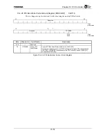
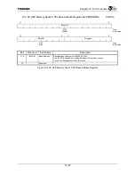
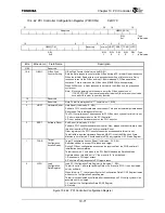
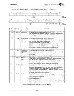
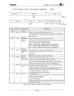
10.4.42 PCI Controller Configuration Register (PCICCFG)
0xD170
31
20
19
16
Reserved GBWC[19:16]
R/W
: Type
0xf
:
Initial
value
15 8 7 5 4 3 2 1 0
GBWC[7:0] Reserved
Reserved
HRST SRST TCAR LCFG
R/W
R/W R/W R/W R/W R/W
:
Type
0xff
1 0 0 0 1
:
Initial
value
Bits Mnemonic Field
Name
Description
31:20
⎯
Reserved
⎯
19:8 GBWC
G-Bus Wait
Counter Setting
G Bus Wait Counter (Initial value: 0xfff, R/W)
Sets the Retry response counter at the G-Bus during a PCI initiator Read transaction.
When the initiator Read access cycle exceeds the setting of this counter, a Retry
response is sent to the G-Bus and the G-Bus is released. PCI Read operation
continues. This counter uses the G-Bus clock (GBUSCLK) when operating.
When 0x000 is set, a Retry response is not sent to the G-Bus by a long response
cycle count.
Note: Since the initial value is the same as for the G-Bus timeout count
(TOCNT.GTOCNT), set the value smaller than the G-Bus timeout count value
such as 0xff0 in order to use retry function.
7:5
⎯
Reserved
⎯
4
⎯
Reserved
Note: This bit is always set to “1”. (Initial value: 1, R/W)
3
HRST
Hardware Reset
Hard Reset (Initial value: 0, R/W)
Performs PCI Controller hardware reset control. This bit is automatically cleared when
Reset ends. This is a diagnostic function.
The PCI Controller cannot be accessed for 32 G-Bus clock cycles after this bit is set.
1: Perform a hardware reset on the PCI Controller.
0: Do not perform a hardware reset on the PCI Controller.
2
SRST
Software Reset
Soft Reset (Initial value: 0, R/W)
Performs PCI Controller software reset control. Also, please use the software to clear
this bit at least four PCI Bus Clock cycles after Reset.
Other registers of the PCI Controller cannot be accessed while this bit is set.
This bit differs from the Hardware Reset bit (HRST) in that the G-Bus Ack State
Machine is not affected. Should be able to R/W any registers. G2P Status Register
1 TCAR
Target
Configuration
Access Ready
Target Configuration Access Ready (Initial value: 0/1, R/W)
Specifies whether to accept PCI access as a target.
During PCI boot, configuration access can be received from the PCI Bus after all
initialization has completed.
This bit becomes “1” only when in the PCI Boot Mode and the Satellite Mode.
Operation when this bit is set to “1” then reset to “0” is not defined.
1: Responds to PCI target access.
0: Performs a Retry response to PCI target access.
0 LCFG
Load
Configuration
Data Register
Load PCI Configuration Data Register (Initial value: 1, R/W)
This bit is set to 1 after reset including Hard or Soft reset in PCIC. It can be cleared
only by software.
When this bit is “1”, the value written to the Configuration Data 0/1/2/3 Register is also
written to the Configuration Space Register.
This bit must be cleared by software after load because no PCI config cycles will be
possible until it is cleared.
1: Load from the Configuration Data 0/1/2/3 Register.
0: No Load.
Figure 10.4.42 PCI Controller Configuration Register
Summary of Contents for TMPR4925
Page 1: ...64 Bit TX System RISC TX49 Family TMPR4925 Rev 3 0 ...
Page 4: ......
Page 15: ...Handling Precautions ...
Page 16: ......
Page 18: ...1 Using Toshiba Semiconductors Safely 1 2 ...
Page 40: ...3 General Safety Precautions and Usage Considerations 3 18 ...
Page 42: ...4 Precautions and Usage Considerations 4 2 ...
Page 43: ...TMPR4925 ...
Page 44: ......
Page 54: ...Chapter 1 Features 1 8 ...
Page 58: ...Chapter 2 Block Diagram 2 4 ...
Page 88: ...Chapter 4 Address Mapping 4 12 ...
Page 226: ...Chapter 8 DMA Controller 8 58 ...
Page 260: ...Chapter 9 SDRAM Controller 9 34 ...
Page 480: ...Chapter 15 Interrupt Controller 15 32 ...
Page 554: ...Chapter 19 Real Time Clock RTC 19 8 ...
Page 555: ...Chapter 20 Removed 20 1 20 Removed ...
Page 556: ...Chapter 20 Removed 20 2 ...
Page 564: ...Chapter 21 Extended EJTAG Interface 21 8 ...
Page 580: ...Chapter 22 Electrical Characteristics 22 16 ...
Page 588: ...Chapter 24 Usage Notes 24 2 ...

