Chapter 16 CHI Module
16-18
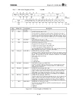
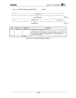
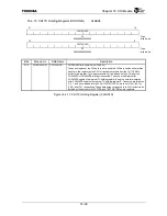
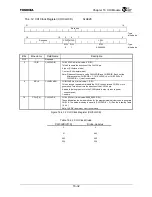
16.4.1 CHI Control Register (CTRL)
0xA800
31 30 29 28 27 26 25 24
20 19
16
Reserved LOOP
TEST
FDIR
FWID
CHAN
TBOF
R/W
R/W
R/W R/W
R/W
R/W
:
Type
0
0
0
00
00000
0000
: Initial value
15 12
11
10 9 8 7 6 5 4 3 2 1 0
RBOF TMSB
RMSB
RFPL TFPL REDG TEDG FEDG TFED
C2X
REN
TEN
CEN
R/W
R/W R/W R/W R/W R/W R/W R/W R/W R/W R/W R/W R/W
:
Type
0000
0 0 0 0 0 0 0 0 0 0 0 0
:
Initial
value
Bits Mnemonic Field
Name
Description
31:30
⎯
Reserved
⎯
29
LOOP
CHILOOP
CHILOOP bit (Initial value: 0, R/W)
This bit is used for IC testing and should not be set. Setting this bit to a logic “1”
will cause the CHI serial transmitted data to be internally looped back to the CHI
serial receive data path. The data is inverted when this mode is selected. Clearing
this bit to a logic “0” selects the normal CHIDIN pin as the CHI serial receive data
source.
28
TEST
CHIENTEST
CHIENTEST bit (Initial value: 0, R/W)
This bit is used for IC testing and should not be set.
27
FDIR
CHIFSDIR
CHIFSDIR bit (Initial value: 0, R/W)
This bit controls the direction of the CHIFS pin.
0: CHIFS to be an input.(CHI sync slave mode) Note
*
1: CHIFS to be an output.(CHI sync master mode)
Note that CHIRXFSPOL and CHIFSEDGE bits must be set to proper values even
when CHIFSDIR is set to a logic “1” (CHI sync master mode).
26:25
FWID[1:0]
CHIFSWIDTH
CHIFSWIDTH bits (Initial value: 00, R/W)
These bits are used to select pulse width for the CHIFS signal, relevant whenever
the CHI Module is configured as master mode. The pulse width is counted by data
bit width. (In clk2x mode, two CHICLKs correspond to one data bit.) The available
CHIFS pulse widths are as follows
00: 1 bit wide
01: 2 bits wides
10: 1 byte wide
11: half-frame wide
24:20
CHAN[4:0]
CHINCHAN
CHINCHAN bits (Initial value: 00000, R/W)
These bits are used to program the number of 8-bit channel timeslots per half-
frame, up to 32 total per half-frame. The value loaded for CHINCHAN is the
desired number of channels-1.
19:16
TBOF[3:0]
CHTXBOFF
CHITXBOFF bits (Initial value: 0000, R/W)
These bits select the transmit data programmable bit offset, which is related to the
number of clocks from the start of timeslot 0 (1st timeslot) transmit data to the
CHIFS edge used to trigger the start of each CHI frame. The value loaded for
CHITXBOFF must be chosen from Table 16.3.3 according to the configuration.
15:12
RBOF[3:0]
CHIRXBOFF
CHIRXBOFF bits (Initial value: 0000, R/W)
These bits select the receive data programmable bit offset, which is related to the
number of clocks from the start of timeslot 0 (1st timeslot) receive data to the
CHIFS edge used to trigger the start of each CHI frame. The value loaded for
CHIRXBOFF must be chosen from Table 16.3.2 according to the configuration.
11
TMSB
TXMSBFIRST
TXMSBFIRST bit (Initial value: 0, R/W)
This bit selects between MSB-first and LSB-first serial data formats for each byte
of the CHI transmit data.
0: LSB-first
1: MSB-first
Figure 16.4.1 Control Register (CTRLREG) (1/3)
Summary of Contents for TMPR4925
Page 1: ...64 Bit TX System RISC TX49 Family TMPR4925 Rev 3 0 ...
Page 4: ......
Page 15: ...Handling Precautions ...
Page 16: ......
Page 18: ...1 Using Toshiba Semiconductors Safely 1 2 ...
Page 40: ...3 General Safety Precautions and Usage Considerations 3 18 ...
Page 42: ...4 Precautions and Usage Considerations 4 2 ...
Page 43: ...TMPR4925 ...
Page 44: ......
Page 54: ...Chapter 1 Features 1 8 ...
Page 58: ...Chapter 2 Block Diagram 2 4 ...
Page 88: ...Chapter 4 Address Mapping 4 12 ...
Page 226: ...Chapter 8 DMA Controller 8 58 ...
Page 260: ...Chapter 9 SDRAM Controller 9 34 ...
Page 480: ...Chapter 15 Interrupt Controller 15 32 ...
Page 554: ...Chapter 19 Real Time Clock RTC 19 8 ...
Page 555: ...Chapter 20 Removed 20 1 20 Removed ...
Page 556: ...Chapter 20 Removed 20 2 ...
Page 564: ...Chapter 21 Extended EJTAG Interface 21 8 ...
Page 580: ...Chapter 22 Electrical Characteristics 22 16 ...
Page 588: ...Chapter 24 Usage Notes 24 2 ...

