Chapter 11 Serial I/O Port
11-21
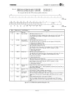
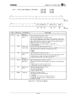
11.4.6 Flow Control Register 0 (SIFLCR0)
0xF314 (Ch. 0)
Flow Control Register 1 (SIFLCR1)
0xF414 (Ch. 1)
31
16
0
:
Type
:
Initial
value
15 13
12
11
10 9 8 7 6 5 4 1 0
0 RCS
TES
0
RTSSC
RSDE TSDE
0 RTSTL
TBRK
R/W
R/W
R/W
R/W
R/W
R/W
R/W
:
Type
0
0 0
1
1
0001
0
:
Initial
value
Bits Mnemonic Field
Name
Description
31:13
⎯
Reserved
⎯
12 RCS
RTS Signal
Control Select
RTS Control Select (Initial value: 0, R/W)
This field sets the reception flow control using RTS output signals.
0: Disable flow control using RTS signals.
1: Enable flow control using RTS signals.
11 TES
CTS Signal
Control Select
CTS Control Select (Initial value: 0, R/W)
This field sets the transmission flow control using CTS input signals.
0: Disable flow control using CTS signals.
1: Enable flow control using CTS signals.
10
⎯
Reserved
⎯
9 RTSSC
RTS
Software
Control
RTS Software Control (Initial value: 0, R/W)
This register is used for software control of RTS output signals.
0: Set the RTS signal to Low (can receive data).
1: Sets the RTS signal to High (transmission pause request)
8 RSDE
Serial Data
Reception
Enable
Receive Serial Data Enable (Initial value: 1, R/W)
This is the Serial Data Enable bit. When this bit is cleared, data reception starts
after the start bit is detected. The RTS signal will not become High even if this bit is
cleared.
0: Enable (can receive data)
1: Disable (halt reception)
7 TSDE
Serial Data
Transmit Enable
Transmit Serial Data Enable (Initial value: 1, R/W)
This is the Serial Data Transmission Enable bit. When this bit is cleared, data
transmission starts. When set, transmission stops after completing transmission of
the current frame.
0: Enable (can transmit data)
1: Disable (halt transmission)
6:5
⎯
Reserved
⎯
4:1 RTSTL
RTS Active
Trigger Level
RTS Trigger Level (Initial value: 0001, R/W)
The RTS hardware control assert level is set by the reception data stage count of
the Receive FIFO.
0000: Disable setting
0001: 1
:
1111: 15
0 TBRK
Break
Transmission
Break Transmit (Initial value: 0, R/W)
Transmits a break. The TXD signal is Low while TBRK is set to “1”.
0: Disable (clear break)
1: Enable (transmit break)
Figure 11.4.6 Flow Control Register
Summary of Contents for TMPR4925
Page 1: ...64 Bit TX System RISC TX49 Family TMPR4925 Rev 3 0 ...
Page 4: ......
Page 15: ...Handling Precautions ...
Page 16: ......
Page 18: ...1 Using Toshiba Semiconductors Safely 1 2 ...
Page 40: ...3 General Safety Precautions and Usage Considerations 3 18 ...
Page 42: ...4 Precautions and Usage Considerations 4 2 ...
Page 43: ...TMPR4925 ...
Page 44: ......
Page 54: ...Chapter 1 Features 1 8 ...
Page 58: ...Chapter 2 Block Diagram 2 4 ...
Page 88: ...Chapter 4 Address Mapping 4 12 ...
Page 226: ...Chapter 8 DMA Controller 8 58 ...
Page 260: ...Chapter 9 SDRAM Controller 9 34 ...
Page 480: ...Chapter 15 Interrupt Controller 15 32 ...
Page 554: ...Chapter 19 Real Time Clock RTC 19 8 ...
Page 555: ...Chapter 20 Removed 20 1 20 Removed ...
Page 556: ...Chapter 20 Removed 20 2 ...
Page 564: ...Chapter 21 Extended EJTAG Interface 21 8 ...
Page 580: ...Chapter 22 Electrical Characteristics 22 16 ...
Page 588: ...Chapter 24 Usage Notes 24 2 ...

