Chapter 11 Serial I/O Port
11-15
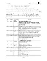
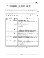
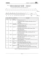
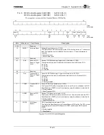
11.4.2 DMA/Interrupt Control Register 0 (SIDICR0)
0xF304 (Ch. 0)
DMA/Interrupt Control Register 1 (SIDICR1)
0xF404 (Ch. 1)
These registers use either DMA or interrupts to execute the Host Interface.
31
16
0
:
Type
:
Initial
value
15 14 13 12 11 10 9 8 6 5
0
TDE RDE TIE RIE SPIE
CTSAC
0
STIE
R/W R/W R/W R/W R/W
R/W
R/W
:
Type
0 0 0 0 0
00
000000
:
Initial
value
Bits Mnemonic Field
Name
Description
31:16
⎯
Reserved
⎯
15 TDE
Transmit DMA
Transfer Enable
Transmit DMA Enable (Initial value: 0, R/W)
This field sets whether to use DMA in the method for writing transmission data to
the Transmit FIFO.
0: Do not use DMA.
1: Use DMA.
14 RDE
Receive DMA
Transfer Enable
Receive DMA Enable (Initial value: 0, R/W)
This field sets whether to use DMA in the method for reading reception data from
the Receive FIFO.
0: Do not use DMA.
1: Use DMA.
13 TIE
Transmit Data
Empty Interrupt
Enable
Transmit Data Empty Interrupt Enable (Initial value: 0, R/W)
When there is open space in the Transmit FIFO, this field sets whether to signal an
interrupt. Set “0” when in the DMA Transmit mode (TDE = 1).
0: Do not signal an interrupt when there is open space in the Transmit FIFO.
1: Signal an interrupt when there is open space in the Transmit FIFO.
12 RIE
Reception Data
Full Interrupt
Enable
Receive Data Full Interrupt Enable (Initial value: 0, R/W)
This field sets whether to signal interrupts when reception data is full
(SIDISRn.RDIS = 1) or a reception time out (SIDISRn.TOUT = 1) occurs. Set to “0”
when in the DMA Receive mode (RDE = 1).
0: Do not signal interrupts when reception data is full/reception time out occurred.
1: Signal interrupts when reception data is full/reception time out occurred.
11 SPIE
Reception Error
Interrupt Enable
Receive Data Error Interrupt Enable (Initial value: 0, R/W)
This field sets whether to signal interrupts when a reception error (Frame Error,
Parity Error, Overrun Error) occurs (SIDISR.ERI = 1).
0: Do not signal reception error interrupts.
1: Signal reception error interrupts.
10:9 CTSAC
CTSS Active
Condition
CTSS Active Condition (Initial value: 00, R/W)
This field specifies status change interrupt request conditions using the CTS Status
(CTSS) of the Status Change Interrupt Status Register.
00: Do not detect CTS signal changes.
01: Rising edge of the CTS pin
10: Falling edge of the CTS pin
11: Both edges of the CTS pin
8:6
⎯
Reserved
⎯
Figure 11.4.2 DMA/Interrupt Control Register (1/2)
Summary of Contents for TMPR4925
Page 1: ...64 Bit TX System RISC TX49 Family TMPR4925 Rev 3 0 ...
Page 4: ......
Page 15: ...Handling Precautions ...
Page 16: ......
Page 18: ...1 Using Toshiba Semiconductors Safely 1 2 ...
Page 40: ...3 General Safety Precautions and Usage Considerations 3 18 ...
Page 42: ...4 Precautions and Usage Considerations 4 2 ...
Page 43: ...TMPR4925 ...
Page 44: ......
Page 54: ...Chapter 1 Features 1 8 ...
Page 58: ...Chapter 2 Block Diagram 2 4 ...
Page 88: ...Chapter 4 Address Mapping 4 12 ...
Page 226: ...Chapter 8 DMA Controller 8 58 ...
Page 260: ...Chapter 9 SDRAM Controller 9 34 ...
Page 480: ...Chapter 15 Interrupt Controller 15 32 ...
Page 554: ...Chapter 19 Real Time Clock RTC 19 8 ...
Page 555: ...Chapter 20 Removed 20 1 20 Removed ...
Page 556: ...Chapter 20 Removed 20 2 ...
Page 564: ...Chapter 21 Extended EJTAG Interface 21 8 ...
Page 580: ...Chapter 22 Electrical Characteristics 22 16 ...
Page 588: ...Chapter 24 Usage Notes 24 2 ...

