Chapter 10 PCI Controller
10-11
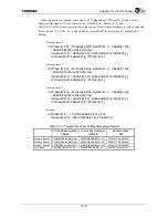
When expressed as a formula, conversion of a PCI Bus Address (PCIAddr[31:0]) into a G-Bus
address (GBusAddr[31:0]) is as follows below. GBASE[31:8], PBASE[31:8], and
AM[28:20]/AM[15:8] each represent the setting register of the corresponding access window indicated
below in Table 10.3.4. The “&” symbol indicates a logical AND for each bit, and “|” indicates bit
linking.
Memory space 0
If (PCIAddr[31:29] | ( PCIAddr[28:20] & !AM[28:20] ) == PBASE[31:29] |
( PBASE[28:20] & !AM[28:20])) then
GBusAddr[31:0] = GBASE[31:29] | ((GBASE[28:20] & !AM[28:20]) ||
(PCIAddr[28:20] & AM[28:20])) | PCIAddr[19:0];
Memory space 1
If (PCIAddr[31:29] | ( PCIAddr[28:20] & !AM[28:20] ) == PBASE[31:29] |
( PBASE[28:20] & !AM[28:20])) then
GBusAddr[31:0] = GBASE[31:29] | ((GBASE[28:20] & !AM[28:20]) ||
(PCIAddr[28:20] & AM[28:20])) | PCIAddr[19:0];
Memory space 2
If (PCIAddr[31:29] | ( PCIAddr[28:20] & !AM[28:20] ) == PBASE[31:29] |
( PBASE[28:20] & !AM[28:20])) then
GBusAddr[31:0] = GBASE[31:29] | ((GBASE[28:20] & !AM[28:20]) ||
(PCIAddr[28:20] & AM[28:20])) | PCIAddr[19:0];
I/O space
If (PCIAddr[31:8] == P2GIOPBASE.BA[31:8]) then
GBusAddr[31:0] = P2GIOGBASE[31:8] | PCIAddr[7:0];
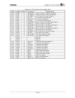
Table 10.3.4 Target Access Space Address Mapping Register
PCI Bus Base Address
PBASE
G-Bus Base Address
GBASE
Address Mask
AM
Memory Space 0 P2GM0PLBASE.BA[31:20]
P2GM0GBASE.BA[31:20]
P2GM0CTR.AM[28:20]
Memory Space 1 P2GM1PLBASE.BA[31:20]
P2GM1GBASE.BA[31:20]
P2GM1CTR.AM[28:20]
Memory Space 2 P2GM2PBASE.BA[31:20]
P2GM2GBASE.BA[31:20]
P2GM2CTR.AM[28:20]
I/O Space
P2GIOPBASE.BA[31:8]
P2GIOGBASE.BA[31:8]
P2GIOCTR.AM[15:8]
Summary of Contents for TMPR4925
Page 1: ...64 Bit TX System RISC TX49 Family TMPR4925 Rev 3 0 ...
Page 4: ......
Page 15: ...Handling Precautions ...
Page 16: ......
Page 18: ...1 Using Toshiba Semiconductors Safely 1 2 ...
Page 40: ...3 General Safety Precautions and Usage Considerations 3 18 ...
Page 42: ...4 Precautions and Usage Considerations 4 2 ...
Page 43: ...TMPR4925 ...
Page 44: ......
Page 54: ...Chapter 1 Features 1 8 ...
Page 58: ...Chapter 2 Block Diagram 2 4 ...
Page 88: ...Chapter 4 Address Mapping 4 12 ...
Page 226: ...Chapter 8 DMA Controller 8 58 ...
Page 260: ...Chapter 9 SDRAM Controller 9 34 ...
Page 480: ...Chapter 15 Interrupt Controller 15 32 ...
Page 554: ...Chapter 19 Real Time Clock RTC 19 8 ...
Page 555: ...Chapter 20 Removed 20 1 20 Removed ...
Page 556: ...Chapter 20 Removed 20 2 ...
Page 564: ...Chapter 21 Extended EJTAG Interface 21 8 ...
Page 580: ...Chapter 22 Electrical Characteristics 22 16 ...
Page 588: ...Chapter 24 Usage Notes 24 2 ...

