Chapter 9 SDRAM Controller
9-15
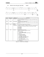
9.4.2
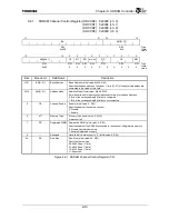
SDRAM Timing Register (SDCTR)
0x8020
31 29 28 27 26 25 24 23 22
18 17 16
BC
ACP PT
RCD
ACE
PDAE
RC
CASL
DRB
R/W
R/W R/W
R/W
R/W
R/W
R/W
R/W
R/W
:
Type
101
11
1
1
0
0 00000 1
0
: Initial
value
15
14
13
12
11
0
DA
SWB
DIA
RP
R/W
R/W R/W R/W
:
Type
1
1 11
0x270
: Initial
value
Bits Mnemonic Field
Name
Description
31:29
BC
Bank Cycle Time
Bank Cycle Time (t
RC
) (Initial value: 101, R/W)
Specifies the bank cycle time.
(
*
2)
000: 5 t
CK
(
*
1)
100: 9 t
CK
001: 6 t
CK
101: 10 t
CK
010: 7 t
CK
110:
Reserved
011: 8 t
CK
111:
Reserved
28:27 ACP
Active Command
Time
Active Command Period (tRAS) (Initial value: 11, R/W)
Specifies the active command time.
00: 3 t
CK
01: 4 t
CK
10: 5 t
CK
11: 6 t
CK
26
PT
Precharge Time
Precharge Time (tRP) (Initial value: 1, R/W)
Specifies the precharge time.
0: 2 t
CK
1: 3 t
CK
25
RCD
RAS-CAS Delay
RAS to CAS Delay (tRCD) (Initial value: 1, R/W)
Specifies the RAS - CAS delay.
0: 2 t
CK
1: 3 t
CK
24
ACE
Advanced CKE
Advanced CKE enable (Initial value: 0, R/W)
Enabling this function makes the timing at which CKE changes one cycle earlier.
0: Disable
1: Enable
23 PDAE
Power
Down
Auto Entry
Power Down Auto Entry Enable (Initial value: 0, R/W)
Enabling this function makes CKE become “L” while the SDRAMC is in the Idle
state. When refresh, memory access, or command execution is performed, CKE
automatically becomes “H”, the requested operation is performed, then CKE returns
to “L” when the operation is complete.
0: Disable
1: Enable
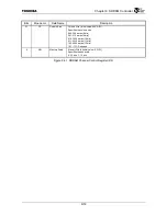
Figure 9.4.2 SDRAM Timing Register (1/2)
Summary of Contents for TMPR4925
Page 1: ...64 Bit TX System RISC TX49 Family TMPR4925 Rev 3 0 ...
Page 4: ......
Page 15: ...Handling Precautions ...
Page 16: ......
Page 18: ...1 Using Toshiba Semiconductors Safely 1 2 ...
Page 40: ...3 General Safety Precautions and Usage Considerations 3 18 ...
Page 42: ...4 Precautions and Usage Considerations 4 2 ...
Page 43: ...TMPR4925 ...
Page 44: ......
Page 54: ...Chapter 1 Features 1 8 ...
Page 58: ...Chapter 2 Block Diagram 2 4 ...
Page 88: ...Chapter 4 Address Mapping 4 12 ...
Page 226: ...Chapter 8 DMA Controller 8 58 ...
Page 260: ...Chapter 9 SDRAM Controller 9 34 ...
Page 480: ...Chapter 15 Interrupt Controller 15 32 ...
Page 554: ...Chapter 19 Real Time Clock RTC 19 8 ...
Page 555: ...Chapter 20 Removed 20 1 20 Removed ...
Page 556: ...Chapter 20 Removed 20 2 ...
Page 564: ...Chapter 21 Extended EJTAG Interface 21 8 ...
Page 580: ...Chapter 22 Electrical Characteristics 22 16 ...
Page 588: ...Chapter 24 Usage Notes 24 2 ...

