Chapter 3 Signals
3-1
3. Signals
3.1 Pin
Signal
Description
In the following tables, asterisks at the end of signal names indicate active-low signals.
In the Type column, PU indicates that the pin is equipped with an internal pull-up resister and PD indicates
that the pin is equipped with an internal pull-down resister. OD indicates an open-drain pin.
The Initial State column shows the state of the signal when the RESET* signal is asserted and
immediately after it is deasserted. Those signals which are selected by a configuration signal upon a reset
have the state selected by the configuration signal even when the reset signal is asserted.
3.1.1
Signals Common to SDRAM and External Bus Interfaces
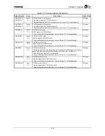
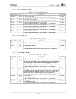
Table 3.1.1 Signals Common to SDRAM and External Bus Interfaces
Signal Name
Type
Description
Initial State
ADDR[19:0] Input/output
PU
Address
Address signals.
For SDRAM, ADDR[19:16 , 14:5] and SADDR10 are used (refer to Sections “9.3.2.2”
and “9.3.2.3 Address Signal Mapping”).
When the external bus controller uses these pins, the meaning of each bit varies with
the data bus width (refer to Section “7.3.5 Data Bus Size”).
The ADDR signals are also used as boot configuration signals (input) during a reset.
For details of configuration signals, refer to Section “3.2 Boot Configuration”.
The ADDR signals are input signals only when the RESET
*
signal is asserted and
become output signals after the RESET
*
signal is deasserted.
Input
SADDR10 Input/output
PU
Address10 for SDRAM
Address signal for SDRAM (refer to Sections “9.3.2.2” and “9.3.2.3 Address Signal
Mapping”).
This signal is also used as a boot configuration input signal for testing. Because this
signal is used for testing, ensure that it will not pulled Low during a reset sequence.
For details of configuration signals, refer to Section “3.2 Boot Configuration”.
This signal is used as an input signal while the RESET
*
signal is asserted. It becomes
an output signal once the RESET
*
signal has been deasserted.
Input
DATA[31:0] Input/output
PU
Data
32-bit data bus.
Input
BUSSPRT Output
Bus
Separate
Controls the connection and separation of devices controlled by the external bus
controller to or from a high-speed device, such as SDRAM (refer to Section “7.6 Flash
ROM, SRAM Usage Example”).
H: Separate devices other than SDRAM from the data bus.
L: Connect devices other than SDRAM to the data bus.
Separation and connection are performed using external bidirectional bus buffers
(such as the 74xx245).
High
Summary of Contents for TMPR4925
Page 1: ...64 Bit TX System RISC TX49 Family TMPR4925 Rev 3 0 ...
Page 4: ......
Page 15: ...Handling Precautions ...
Page 16: ......
Page 18: ...1 Using Toshiba Semiconductors Safely 1 2 ...
Page 40: ...3 General Safety Precautions and Usage Considerations 3 18 ...
Page 42: ...4 Precautions and Usage Considerations 4 2 ...
Page 43: ...TMPR4925 ...
Page 44: ......
Page 54: ...Chapter 1 Features 1 8 ...
Page 58: ...Chapter 2 Block Diagram 2 4 ...
Page 88: ...Chapter 4 Address Mapping 4 12 ...
Page 226: ...Chapter 8 DMA Controller 8 58 ...
Page 260: ...Chapter 9 SDRAM Controller 9 34 ...
Page 480: ...Chapter 15 Interrupt Controller 15 32 ...
Page 554: ...Chapter 19 Real Time Clock RTC 19 8 ...
Page 555: ...Chapter 20 Removed 20 1 20 Removed ...
Page 556: ...Chapter 20 Removed 20 2 ...
Page 564: ...Chapter 21 Extended EJTAG Interface 21 8 ...
Page 580: ...Chapter 22 Electrical Characteristics 22 16 ...
Page 588: ...Chapter 24 Usage Notes 24 2 ...


