Chapter 3 Signals
3-15
3.3 Pin
Multiplexing
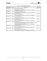
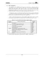
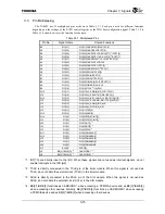
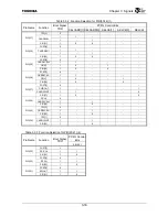
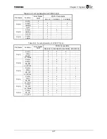
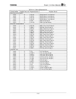
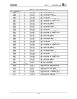
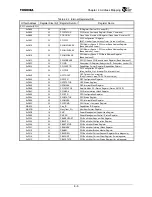
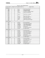
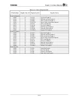
The TX4925 has 35 multiplexed pins as shown in Table 3.3.1. Each pin is used for different functions
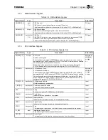
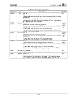
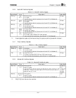
depending on the settings of the PCFG control register or the TDO boot configuration signal. Table 3.3.2 to
Table 3.3.8 show how to set the function for each pin.
Table 3.3.1 Multiplexed Pins
Pin No.
Signal Name
Shared Functions
B5 PIO[31]
PIO[31]/CARDDIR
*
/BCLK/TPC[2]
D6 PIO[30]
PIO[30]/CARDREG
*
/PCST[8]
B6 PIO[29]
PIO[29]/CARD2CSH
*
/CE5
*
/INT[7]
*
1
/PCST[6]
C6 PIO[28]
PIO[28]/CARD2CSL
*
/CE4
*
/INT[6]
*
1
/PCST[7]
A6 PIO[27]
PIO[27]/CARD2WAIT
*
*
2
/CHIOUT/PCST[5]
A4 PIO[26]
PIO[26]/CARD1CSH
*
/DCLK
C5 PIO[25]
PIO[25]/CARD1CSL
*
/TPC[3]
A5 PIO[24]
PIO[24]/CARD1WAIT
*
*
2
/TPC[1]
C8 PIO[23]
PIO[23]/SPICLK/PCST[2]
A7 PIO[22]
PIO[22]/SPIIN/PCST[3]
B7 PIO[21]
PIO[21]/SPIOUT/PCST[4]
B9 PIO[20]
PIO[20]/TIMER[0]/CHIFS/PCST[1]
A8 PIO[19]
PIO[19]/TIMER[1]/CHICLK
B8 PIO[18]
PIO[18]/TCLK
*
2
/CHIDIN
W15 PIO[17]
PIO[17]/AC_SDIN[0]/ND_WE
*
/TXD[1]
V16 PIO[16]
PIO[16]/AC_SDOUT/ND_RB
*
/RXD[1]
W16 PIO[15]
PIO[15]/AC_BITCLK/ND_CLE/RTS[1]/INT[5]
*
1
Y16 PIO[14]
PIO[14]/AC_SYNC/ND_RE
*
/CTS[1]/INT[4]
*
1
V15 PIO[13]
PIO[13]/AC_SDIN[1]/ND_ALE
Y15 PIO[12]
PIO[12]/AC_RST
*
/ND_CE
*
Y13 PIO[11]
PIO[11]/TXD[0]
W13 PIO[10]
PIO[10]/RXD[0]
W14 PIO[9]
PIO[9]/RTS[0]
*
/INT[3]
*
1
Y14 PIO[8]
PIO[8]/CTS[0]
*
/INT[2]
*
1
U15 PIO[7]
PIO[7]/INT[1]
*
1
U13 PIO[6]
PIO[6]/INT[0]
*
1
V13 PIO[5]
PIO[5]/SCLK
*
3
W11 PIO[4]
PIO[4]/DMAACK[1]
W12 PIO[3]
PIO[3]/DMAREQ[1]
V10 PIO[2]
PIO[2]/DMAACK[0]
V12 PIO[1]
PIO[1]/DMAREQ[0]
U10 PIO[0]
PIO[0]/DMADONE
Y17 BC32K
PCST[0]
V6 BE[3]
*
/BWE[3]
*
*
4
CARDIORD
*
*
4
U6 BE[2]
*
/BWE[2]
*
*
4
CARDIOWR
*
*
4
*
1: INT[7:0] are directly input to the IRC. When these signals are not used as interrupt signals, do not
enable interrupts in the IRC.[m2]
*
2: TCLK is directly connected to the TCLK pin of the timer module. When this signal is not used as
TCLK, do not enable the external clock (TCLK) in the timer module.
*
3: SCLK is directly connected to the SCLK pin of the SIO module. When this signal is not used as
SCLK, do not enable the external clock (SCLK) in the SIO module.
*
4: BE[3]
*
/BWE[3] functions as CARDIORD
*
when accessing a PCMCIA device and as BE[3]
*
/BWE[3]
when accessing other devices. Similarly, BE[2]
*
/BWE[2] functions as CARDIOWR
*
when accessing
a PCMCIA device and as BE[2]
*
/BWE[2] when accessing other devices.
Summary of Contents for TMPR4925
Page 1: ...64 Bit TX System RISC TX49 Family TMPR4925 Rev 3 0 ...
Page 4: ......
Page 15: ...Handling Precautions ...
Page 16: ......
Page 18: ...1 Using Toshiba Semiconductors Safely 1 2 ...
Page 40: ...3 General Safety Precautions and Usage Considerations 3 18 ...
Page 42: ...4 Precautions and Usage Considerations 4 2 ...
Page 43: ...TMPR4925 ...
Page 44: ......
Page 54: ...Chapter 1 Features 1 8 ...
Page 58: ...Chapter 2 Block Diagram 2 4 ...
Page 88: ...Chapter 4 Address Mapping 4 12 ...
Page 226: ...Chapter 8 DMA Controller 8 58 ...
Page 260: ...Chapter 9 SDRAM Controller 9 34 ...
Page 480: ...Chapter 15 Interrupt Controller 15 32 ...
Page 554: ...Chapter 19 Real Time Clock RTC 19 8 ...
Page 555: ...Chapter 20 Removed 20 1 20 Removed ...
Page 556: ...Chapter 20 Removed 20 2 ...
Page 564: ...Chapter 21 Extended EJTAG Interface 21 8 ...
Page 580: ...Chapter 22 Electrical Characteristics 22 16 ...
Page 588: ...Chapter 24 Usage Notes 24 2 ...


