Chapter 3 Signals
3-12
3.2 Boot
Configuration
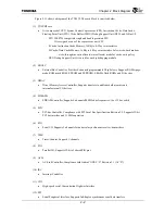
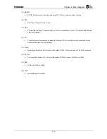
The ADDR[19:0], UAE, SADDR10 and TDO signals can also function as configuration signals for
initially setting various functions upon booting the system. The states of the configuration signals
immediately after the RESET* or PON* signal is deasserted are read as initial values for the TX4925
internal registers. A High signal level sets a value of 1 and a Low signal level sets a value of 0. UAE,
SADDR10 and ADDR[17,16,10] are used for testing. Ensure that these pins will not set to 0.
All configuration signals are provided with internal pull-up resistors. To drive a signal Low, pull down the
corresponding pin on the board using an approx. 4.7 k
Ω
resistor. Driving a signal High does not require a
pull-down resistor. Any signals defined as Reserved should not be pulled down.
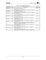
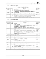
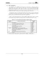
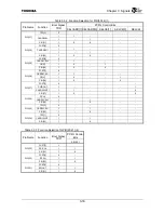
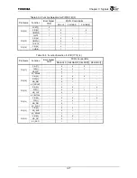
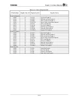
Table 3.2.1 lists the functions that can be set using configuration signals. Table 3.2.2 and 3.2.3 describe
each configuration signal. Note that the functions of some pins vary with the boot memory device used.
Table 3.2.1 Functions that Can be Set Using Configuration Signals
Peripheral
Function
Functions that Can be Set
Configuration
Signal
PCICLK enable
ADDR[18]
PCI controller operating mode (satellite or host) ADDR[15]
PCI bus arbiter selection (internal or external)
ADDR[1]
PCI controller
PCI bus master
*
1
ADDR[11]
Division ratio of SYSCLK to GBUSCLK
ADDR[4:3]
Boot device selection
ADDR[8:6]
BE[3:0]
*
/BWE[3:0]
*
function selection upon booting ADDR[11]
Handling of the ACK signal upon booting (internal or external) ADDR[5]
External bus
controller
Data bus width for the boot device
ADDR[13:12]
Endian
setting
ADDR[14]
Others
Controlling built-in timer interrupts of the TX49/H2 core
ADDR[0]
PC
trace
TDO
*
1: Valid when the boot memory device is PCI and the PCIC operates in satellite mode.
Summary of Contents for TMPR4925
Page 1: ...64 Bit TX System RISC TX49 Family TMPR4925 Rev 3 0 ...
Page 4: ......
Page 15: ...Handling Precautions ...
Page 16: ......
Page 18: ...1 Using Toshiba Semiconductors Safely 1 2 ...
Page 40: ...3 General Safety Precautions and Usage Considerations 3 18 ...
Page 42: ...4 Precautions and Usage Considerations 4 2 ...
Page 43: ...TMPR4925 ...
Page 44: ......
Page 54: ...Chapter 1 Features 1 8 ...
Page 58: ...Chapter 2 Block Diagram 2 4 ...
Page 88: ...Chapter 4 Address Mapping 4 12 ...
Page 226: ...Chapter 8 DMA Controller 8 58 ...
Page 260: ...Chapter 9 SDRAM Controller 9 34 ...
Page 480: ...Chapter 15 Interrupt Controller 15 32 ...
Page 554: ...Chapter 19 Real Time Clock RTC 19 8 ...
Page 555: ...Chapter 20 Removed 20 1 20 Removed ...
Page 556: ...Chapter 20 Removed 20 2 ...
Page 564: ...Chapter 21 Extended EJTAG Interface 21 8 ...
Page 580: ...Chapter 22 Electrical Characteristics 22 16 ...
Page 588: ...Chapter 24 Usage Notes 24 2 ...

