Chapter 14 AC-link Controller
14-10
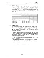
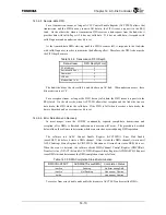
14.3.6.2 DMA Channel Mapping
ACLC uses four DMA request channels. These DMA channels are allocated to four out of
seven data-streams, or slots, on the AC-link frame, according to ACLC DMA Channel Selection
Register (ACDMASEL) setting as shown in Table 14.3.1. The pin configuration register allocates
these DMA channels of ACLC to the DMAC (DMA controller) channels according to DMA
Request Control Register (DRQCTR)’s DMA Request Selection (DMAREQ0-3) bits as described
in section 5.2.8.
Table 14.3.1 DMA Channel Mapping Modes
ACDMASEL
AC-link Slot Number
0
1
2
3
PCM L&R out (3&4)
ACLC ch0
ACLC ch0
ACLC ch0
ACLC ch0
Surround L&R out (7&8)
ACLC ch1
ACLC ch1
ACLC ch1
Center out (6)
ACLC ch2
LFE out (9)
ACLC ch3
ACLC ch3
PCM L&R in (3&4) or Mic in (6)
ACLC ch1
ACLC ch2
Modem Line1 out (5)
ACLC ch2
ACLC ch2
Modem Line 1 in (5)
ACLC ch3
ACLC ch3
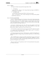
14.3.6.3 Sample-data Format
ACLC transmits/receives 16 bits per sample for each data slot shown in Table 14.3.1. The data
resides on the first 16 bits of the 20 bits assigned to each slot on AC-link. Each sample-data
register allows access by word (32-bit) unit only. Therefore the DMA count must be a multiple of
word. Note that the transmit-data DMA count also must be the FIFO depth (refer to Table 14.3.8)
or more for a reason described later.
For audio PCM front and surround streams, every data-word is loaded with a couple of left and
right samples. For audio MIC stream, valid data is loaded in the same field as the left sample
while the other field is filled with ‘0’. For audio center, LFE, and modem line 1 streams, two
consecutive samples are packed into every word.
The data format at the sample-data register is arranged so that the data format on the DMA
buffer follows the rules below.
•
Each sample data is put in the byte order in which the CPU operates (big- or little-endian).
•
Samples are put in the time-sequential order at increasing addresses on memory.
•
For a DMA channel which couples left and right samples, each left sample precedes the
corresponding right sample.
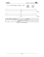
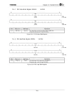
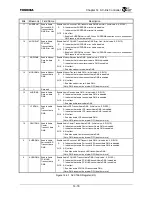
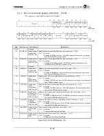
Refer to the sections 14.4.16 and later for the register format.
Summary of Contents for TMPR4925
Page 1: ...64 Bit TX System RISC TX49 Family TMPR4925 Rev 3 0 ...
Page 4: ......
Page 15: ...Handling Precautions ...
Page 16: ......
Page 18: ...1 Using Toshiba Semiconductors Safely 1 2 ...
Page 40: ...3 General Safety Precautions and Usage Considerations 3 18 ...
Page 42: ...4 Precautions and Usage Considerations 4 2 ...
Page 43: ...TMPR4925 ...
Page 44: ......
Page 54: ...Chapter 1 Features 1 8 ...
Page 58: ...Chapter 2 Block Diagram 2 4 ...
Page 88: ...Chapter 4 Address Mapping 4 12 ...
Page 226: ...Chapter 8 DMA Controller 8 58 ...
Page 260: ...Chapter 9 SDRAM Controller 9 34 ...
Page 480: ...Chapter 15 Interrupt Controller 15 32 ...
Page 554: ...Chapter 19 Real Time Clock RTC 19 8 ...
Page 555: ...Chapter 20 Removed 20 1 20 Removed ...
Page 556: ...Chapter 20 Removed 20 2 ...
Page 564: ...Chapter 21 Extended EJTAG Interface 21 8 ...
Page 580: ...Chapter 22 Electrical Characteristics 22 16 ...
Page 588: ...Chapter 24 Usage Notes 24 2 ...

