Chapter 7 External Bus Controller
7-14
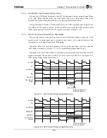
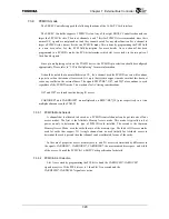
7.3.7.2 ACK
*
/READY Input/Output Switching Timing
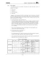
When in the ACK*/Ready Static mode, the ACK*/Ready signal is always an input signal. When
in the ACK*/Ready Dynamic mode, the ACK*/Ready signal is an input signal when in the
External ACK mode or the Ready mode, but is an output signal in all other modes.
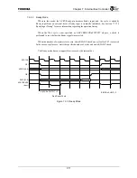
During External ACK mode or Ready mode access, the ACK* signal becomes High-Z at the
cycle where the CE* signal is asserted. At the end of the access cycle, the ACK* signal is output
(driven) again one clock cycle after the CE* signal is deasserted (see Figure 7.3.3).
7.3.7.3 ACK
*
Output Timing (Normal Mode, Page Mode)
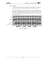
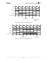
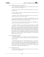
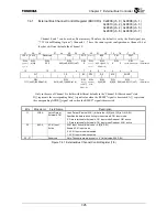
When in the Normal mode and Page mode of the ACK*/Ready Dynamic mode, the ACK*
signal becomes an output signal and is asserted for one clock cycle to send notification to the
external device of the data Read and data Write timing.
During the Read cycle, the data is latched at the rise of the next clock cycle after when the
ACK* signal is asserted. (See Figure 7.3.7 ACK* Output Timing (Single Read Cycle) ).
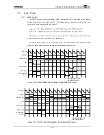
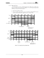
During the Write cycle, SWE*/BWE* is deasserted at the next clock cycle after when the ACK*
signal is deasserted, and the data is held for one more clock cycle after that. (See Figure 7.3.8
ACK* Output Timing (Single Write Cycle) ).
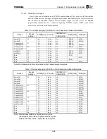
Figure 7.3.7 ACK
*
Output Timing (Single Read Cycle)
Figure 7.3.8 ACK
*
Output Timing (Single Write Cycle)
1 clock
SYSCLK
CE
*
ADDR [19
:
0]
OE
*
DATA [31:0]
ACK
*
/READY
(Output)
Data is latched
EBCCRn.PWT:WT=2
EBCCRn.SHWT=0
SYSCLK
CE
*
ADDR [19
:
0]
SWE
*/
BWE
*
DATA [31
:
0]
ACK
*
/READY
(Output)
2 clocks
EBCCRn.PWT:WT=2
EBCCRn.SHWT=0
1 clock
Summary of Contents for TMPR4925
Page 1: ...64 Bit TX System RISC TX49 Family TMPR4925 Rev 3 0 ...
Page 4: ......
Page 15: ...Handling Precautions ...
Page 16: ......
Page 18: ...1 Using Toshiba Semiconductors Safely 1 2 ...
Page 40: ...3 General Safety Precautions and Usage Considerations 3 18 ...
Page 42: ...4 Precautions and Usage Considerations 4 2 ...
Page 43: ...TMPR4925 ...
Page 44: ......
Page 54: ...Chapter 1 Features 1 8 ...
Page 58: ...Chapter 2 Block Diagram 2 4 ...
Page 88: ...Chapter 4 Address Mapping 4 12 ...
Page 226: ...Chapter 8 DMA Controller 8 58 ...
Page 260: ...Chapter 9 SDRAM Controller 9 34 ...
Page 480: ...Chapter 15 Interrupt Controller 15 32 ...
Page 554: ...Chapter 19 Real Time Clock RTC 19 8 ...
Page 555: ...Chapter 20 Removed 20 1 20 Removed ...
Page 556: ...Chapter 20 Removed 20 2 ...
Page 564: ...Chapter 21 Extended EJTAG Interface 21 8 ...
Page 580: ...Chapter 22 Electrical Characteristics 22 16 ...
Page 588: ...Chapter 24 Usage Notes 24 2 ...


