Chapter 8 DMA Controller
8-17
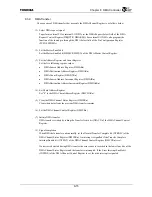
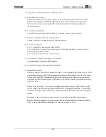
The sequence of Chain DMA transfer is as follows below.
(1) Select DMA request signal
To perform external I/O or internal I/O DMA, set the DMA Request Select field of the DMA
Request Control Register (DRQCTR. DMAREQ). For external I/O DMA, also program the
function of the shared pin through the DMA Select field of the Pin Configuration Register
(PCFG.SELDMA).
(2) Set the Master Enable bit
Set the Master Enable bit (DMMCR.MSTEN) of the DMA Master Control Register.
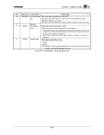
(3) Structure of the DMA command Descriptor chain
Construct the DMA Command Descriptor Chain in memory.
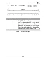
(4) Set the Count Register
Set “0” to the DMA Count Register (DMCNTRn) .
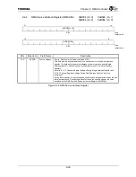
Sets the DMA Source Address Increment Register (DMSAIRn) and DMA destination Address
Increment Register (MMDAIRn).
Never set 0 or less than 0 for the increment value.
(5) Clear the DMA Channel Status Register (DMCSRn)
Clear the status of the previous DMA transfer.
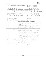
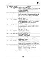
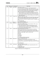
(6) Set the DMA Channel Control Register (DMCCRn).
(7) Initiate DMA transfer
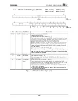
Setting the address of the DMA Command Descriptor at the beginning of the chain list in the DMA
Chain Address Register (DMCHARn) automatically initiates DMA transfer. First, the value stored
in each field of the DMA Command descriptor at the beginning of the Chain List is read to each
corresponding DMA Channel register (Chain transfer), then DMA transfer is performed according
to the read value.
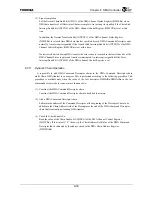
When a value other than “0” is stored in the DMA Chain Address Register (DMCHARn), data of
the size stored in the DMA Count Register (DMCNTRn) is completely transferred, then the DMA
Command Descriptor value of the memory address specified by the DMA Chain Address Register
is read.
In addition, if the Chain Address field value read the Descriptor 0, the DMA Chain Address
Register value is not updated. All previous values (Data Command Descriptor Addresses with the
value “0” in the Chain Address field when the values were read) are held.
Summary of Contents for TMPR4925
Page 1: ...64 Bit TX System RISC TX49 Family TMPR4925 Rev 3 0 ...
Page 4: ......
Page 15: ...Handling Precautions ...
Page 16: ......
Page 18: ...1 Using Toshiba Semiconductors Safely 1 2 ...
Page 40: ...3 General Safety Precautions and Usage Considerations 3 18 ...
Page 42: ...4 Precautions and Usage Considerations 4 2 ...
Page 43: ...TMPR4925 ...
Page 44: ......
Page 54: ...Chapter 1 Features 1 8 ...
Page 58: ...Chapter 2 Block Diagram 2 4 ...
Page 88: ...Chapter 4 Address Mapping 4 12 ...
Page 226: ...Chapter 8 DMA Controller 8 58 ...
Page 260: ...Chapter 9 SDRAM Controller 9 34 ...
Page 480: ...Chapter 15 Interrupt Controller 15 32 ...
Page 554: ...Chapter 19 Real Time Clock RTC 19 8 ...
Page 555: ...Chapter 20 Removed 20 1 20 Removed ...
Page 556: ...Chapter 20 Removed 20 2 ...
Page 564: ...Chapter 21 Extended EJTAG Interface 21 8 ...
Page 580: ...Chapter 22 Electrical Characteristics 22 16 ...
Page 588: ...Chapter 24 Usage Notes 24 2 ...

