Chapter 8 DMA Controller
8-7
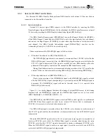
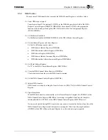
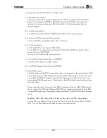
When the Chain End bit (CHDN) is cleared, only DMA transfer specified by the current DMA
Channel Register ends normally, and only the Normal Transfer End bit (NTRNFC) is set. When
the Chain Enable bit (CHNEN) of the DMA Channel Control Register (DMCCRn) is set, chain
transfer is executed and DMA transfer continues. When the Chain Enable bit (CHNEN) is cleared,
the Transfer Active bit (DMCCRn.XFACT) is cleared and the Normal Chain End bit (NCHNC) is
set.
Three clock cycles are required from external assertion of the DMADONE* signal to disabling
of new DMA access. Operation will not stop even if the bus operation in progress is a Single
transfer or a Burst transfer. For example, if the DMADONE* signal is asserted during Read
operation of Dual Address transfer, the corresponding Write bus operation will also be executed.
If the DMADONE* pin is set to become both input and output for channel
n
(DMCCRn.DNCTRL = “11”), the DMADONE* signal becomes an open drain signal when the
channel becomes active. When used by this mode, the DMADONE* signal must be pulled up by
an external source. When in this mode, the External DONE Assert bit (DMCSRn.EXTDN) is not
only set when asserted by an external device, but is also set when asserted by the TX4925.
8.3.4
Internal I/O DMA Transfer Mode
Performs DMA with the on-chip Serial I/O Controller and the AC-link Controller. Set the DMA
Channel Control Register (DMCCRn) as follows.
•
DMCCRn.EXTRQ
=
1: I/O DMA Transfer mode
•
DMCCRn.SNGAD
=
0: Dual Address Transfer
Refer to “8.3.8 Dual Address Transfer” and “11.3.6 DMA transfer (Serial I/O Controller)” or
“14.3.6.4 DMA Operation (AC-link Controller)” for more information.
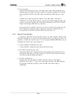
8.3.5
Memory-Memory Copy Mode
It is possible to copy memory from any particular address to any other particular address when in the
Memory-Memory Copy mode.
Set the DMA Channel Control Register (DMCCRn) as follows.
•
DMCCRn.EXTRQ
=
0: Memory Transfer mode
•
DMCCRn.SNGAD
=
0: Dual Address mode
Furthermore, when in the Memory-Memory Copy mode it is possible to set the interval for requesting
ownership of each bus using the Internal Request Delay field (INTRQD) of the DMA Channel Control
Register (DMCCRn).
Refer to “8.3.8 Dual Address Transfer” for information regarding the setting of other registers.
Summary of Contents for TMPR4925
Page 1: ...64 Bit TX System RISC TX49 Family TMPR4925 Rev 3 0 ...
Page 4: ......
Page 15: ...Handling Precautions ...
Page 16: ......
Page 18: ...1 Using Toshiba Semiconductors Safely 1 2 ...
Page 40: ...3 General Safety Precautions and Usage Considerations 3 18 ...
Page 42: ...4 Precautions and Usage Considerations 4 2 ...
Page 43: ...TMPR4925 ...
Page 44: ......
Page 54: ...Chapter 1 Features 1 8 ...
Page 58: ...Chapter 2 Block Diagram 2 4 ...
Page 88: ...Chapter 4 Address Mapping 4 12 ...
Page 226: ...Chapter 8 DMA Controller 8 58 ...
Page 260: ...Chapter 9 SDRAM Controller 9 34 ...
Page 480: ...Chapter 15 Interrupt Controller 15 32 ...
Page 554: ...Chapter 19 Real Time Clock RTC 19 8 ...
Page 555: ...Chapter 20 Removed 20 1 20 Removed ...
Page 556: ...Chapter 20 Removed 20 2 ...
Page 564: ...Chapter 21 Extended EJTAG Interface 21 8 ...
Page 580: ...Chapter 22 Electrical Characteristics 22 16 ...
Page 588: ...Chapter 24 Usage Notes 24 2 ...


