Chapter 10 PCI Controller
10-82
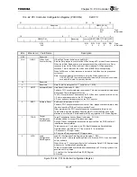
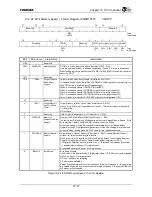
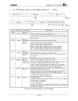
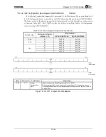
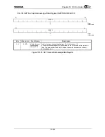
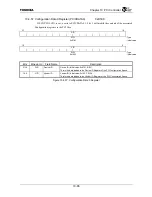
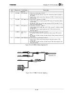
10.4.53 G2P Configuration Address Register(G2PCFGADRS)
0xD1A0[m3]
31
24
23
16
Reserved BUSNUM
R/W
: Type
0x00
:
Initial
value
15 11
10 8 7 2 1 0
DEVNUM
FNNUM
REGNUM
TYPE
R/W
R/W
R/W R/W
:
Type
0x00
000
0x00
00
:
Initial
value
Bits Mnemonic Field
Name
Description
31:24
⎯
Reserved
⎯
23:16
BUSNUM
Bus Number
Bus Number (Initial value: 0x00, R/W)
Indicates the target PCI Bus Number (one of 256).
15:11
DEVNUM
Device Number
Device Number (Initial value: 0x00, R/W)
This field is used to identify the target physical device number. (This is one number
out of 32 devices. 21 of these 32 devices are used.)
When in the address phase of Type 0 configuration access, AD[31:11] of the upper 21
address lines are used as the IDSEL signal.
0x00: Use AD [11] as IDSEL.
0x01: Use AD [12] as IDSEL.
0x02: Use AD [13] as IDSEL.
:
:
0x13: Use AD [30] as IDSEL.
0x14: Use AD [31] as IDSEL.
0x15 - 0x1F: Reserved
10:8
FNNUM
Function Number Function Number (Initial value: 000, R/W)
This field is used to identify the target logic function number (one out of 8).
7:2
REGNUM
Register Number
Register Number (Initial value: 0x00, R/W)
This field is used to identify the DWORD (one out of 64) inside the Configuration
Space of the target function
1:0
TYPE
Type
Type (Initial value: 00, R/W)
This field is used to identify the address type in the address phase of the target
function configuration cycle.
0x0: Type 0 configuration (Use the AD[31:11] signal as the IDSEL signal.)
0x1: Type 1 configuration (Output all bits unchanged as the address to the AD[ ]
signal.)
Figure 10.4.53 G2P Configuration Address Register
Summary of Contents for TMPR4925
Page 1: ...64 Bit TX System RISC TX49 Family TMPR4925 Rev 3 0 ...
Page 4: ......
Page 15: ...Handling Precautions ...
Page 16: ......
Page 18: ...1 Using Toshiba Semiconductors Safely 1 2 ...
Page 40: ...3 General Safety Precautions and Usage Considerations 3 18 ...
Page 42: ...4 Precautions and Usage Considerations 4 2 ...
Page 43: ...TMPR4925 ...
Page 44: ......
Page 54: ...Chapter 1 Features 1 8 ...
Page 58: ...Chapter 2 Block Diagram 2 4 ...
Page 88: ...Chapter 4 Address Mapping 4 12 ...
Page 226: ...Chapter 8 DMA Controller 8 58 ...
Page 260: ...Chapter 9 SDRAM Controller 9 34 ...
Page 480: ...Chapter 15 Interrupt Controller 15 32 ...
Page 554: ...Chapter 19 Real Time Clock RTC 19 8 ...
Page 555: ...Chapter 20 Removed 20 1 20 Removed ...
Page 556: ...Chapter 20 Removed 20 2 ...
Page 564: ...Chapter 21 Extended EJTAG Interface 21 8 ...
Page 580: ...Chapter 22 Electrical Characteristics 22 16 ...
Page 588: ...Chapter 24 Usage Notes 24 2 ...

