Chapter 17 Serial Peripheral Interface
17-6
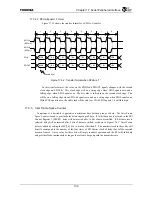
17.3.4.2 SPHA Equals 1 Format
Figure 17.3.2 shows the transfer format for a SPHA=1 transfer.
SPICLK
(SPOL=0)
SPICLK
(SPOL=1)
SPIIN
SPIOUT
MSB
B6
B5
B4
B3
B2
B1
LSB
MSB
B6
B5
B4
B3
B2
B1
LSB
Sample Point
1
2
3
4
5
6
7
8
Figure 17.3.2 Transfer format when SPHA is “1”.
In this transfer format, the value on the SPIIN and SPIOUT signals changes with the second
clock edge on SPICLK. This clock edge will be a rising edge when SPOL equals zero and a
falling edge, when SPOL equals one. The bit value is shifted in on the second clock edge. This
will be on a falling edge when SPOL bit equals zero and on a rising edge when SPOL equals one.
With SPOL equal to zero, the shift clock will be idle low. With SPOL equals 1 it will idle high.
17.3.5 Inter Frame Space Counter
Sometimes it is desirable to guarantee a minimum time between groups of data. The Inter Frame
Space Counter is used to provide delay between groups of data. If 16-bit data size is selected in the SPI
Control Register 1 (SPCR1), delay will be inserted after 16 bits of data are shifted. If 8-bit data size is
selected, delay will be inserted after 8 bits of data are shifted, as shown in Figure 17.4.3. Inter Frame
delay is added by setting the IFS[7:0] bits to a value other than 0. The number stored in these bits will
directly correspond to the number of the four times of SPI Master clock of delay that will be inserted
between frames. A zero value for these bits will imply seamless operation and the SPI will shift data
and provide clocks continuously as long as the software keeps up with the transmitter rate.
Summary of Contents for TMPR4925
Page 1: ...64 Bit TX System RISC TX49 Family TMPR4925 Rev 3 0 ...
Page 4: ......
Page 15: ...Handling Precautions ...
Page 16: ......
Page 18: ...1 Using Toshiba Semiconductors Safely 1 2 ...
Page 40: ...3 General Safety Precautions and Usage Considerations 3 18 ...
Page 42: ...4 Precautions and Usage Considerations 4 2 ...
Page 43: ...TMPR4925 ...
Page 44: ......
Page 54: ...Chapter 1 Features 1 8 ...
Page 58: ...Chapter 2 Block Diagram 2 4 ...
Page 88: ...Chapter 4 Address Mapping 4 12 ...
Page 226: ...Chapter 8 DMA Controller 8 58 ...
Page 260: ...Chapter 9 SDRAM Controller 9 34 ...
Page 480: ...Chapter 15 Interrupt Controller 15 32 ...
Page 554: ...Chapter 19 Real Time Clock RTC 19 8 ...
Page 555: ...Chapter 20 Removed 20 1 20 Removed ...
Page 556: ...Chapter 20 Removed 20 2 ...
Page 564: ...Chapter 21 Extended EJTAG Interface 21 8 ...
Page 580: ...Chapter 22 Electrical Characteristics 22 16 ...
Page 588: ...Chapter 24 Usage Notes 24 2 ...


