3 General Safety Precautions and Usage Considerations
3-8
3.3.8 Thermal
design
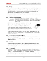
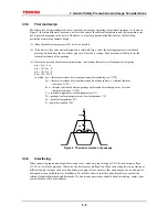
The failure rate of semiconductor devices is greatly increased as operating temperatures increase. As shown in
Figure 2, the internal thermal stress on a device is the sum of the ambient temperature and the temperature rise
due to power dissipation in the device. Therefore, to achieve optimum reliability, observe the following
precautions concerning thermal design:
(1) Keep the ambient temperature (Ta) as low as possible.
(2) If the device’s dynamic power dissipation is relatively large, select the most appropriate circuit board
material, and consider the use of heat sinks or of forced air cooling. Such measures will help lower the
thermal resistance of the package.
(3) Derate the device’s absolute maximum ratings to minimize thermal stress from power dissipation.
θ
ja =
θ
jc +
θ
ca
θ
ja = (Tj–Ta) / P
θ
jc = (Tj–Tc) / P
θ
ca = (Tc–Ta) / P
in which
θ
ja = thermal resistance between junction and surrounding air (°C/W)
θ
jc = thermal resistance between junction and package surface, or internal thermal
resistance
(°C/W)
θ
ca = thermal resistance between package surface and surrounding air, or external
thermal resistance (°C/W)
Tj = junction temperature or chip temperature (°C)
Tc = package surface temperature or case temperature (°C)
Ta = ambient temperature (°C)
P = power dissipation (W)
Tc
θ
ca
Ta
Tj
θ
jc
Figure 2 Thermal resistance of package
3.3.9 Interfacing
When connecting inputs and outputs between devices, make sure input voltage (V
IL
/V
IH
) and output voltage
(V
OL
/V
OH
) levels are matched. Otherwise, the devices may malfunction. When connecting devices operating at
different supply voltages, such as in a dual-power-supply system, be aware that erroneous power-on and power-
off sequences can result in device breakdown. For details of how to interface particular devices, consult the
relevant technical datasheets and databooks. If you have any questions or doubts about interfacing, contact your
nearest Toshiba office or distributor.
Summary of Contents for TMPR4925
Page 1: ...64 Bit TX System RISC TX49 Family TMPR4925 Rev 3 0 ...
Page 4: ......
Page 15: ...Handling Precautions ...
Page 16: ......
Page 18: ...1 Using Toshiba Semiconductors Safely 1 2 ...
Page 40: ...3 General Safety Precautions and Usage Considerations 3 18 ...
Page 42: ...4 Precautions and Usage Considerations 4 2 ...
Page 43: ...TMPR4925 ...
Page 44: ......
Page 54: ...Chapter 1 Features 1 8 ...
Page 58: ...Chapter 2 Block Diagram 2 4 ...
Page 88: ...Chapter 4 Address Mapping 4 12 ...
Page 226: ...Chapter 8 DMA Controller 8 58 ...
Page 260: ...Chapter 9 SDRAM Controller 9 34 ...
Page 480: ...Chapter 15 Interrupt Controller 15 32 ...
Page 554: ...Chapter 19 Real Time Clock RTC 19 8 ...
Page 555: ...Chapter 20 Removed 20 1 20 Removed ...
Page 556: ...Chapter 20 Removed 20 2 ...
Page 564: ...Chapter 21 Extended EJTAG Interface 21 8 ...
Page 580: ...Chapter 22 Electrical Characteristics 22 16 ...
Page 588: ...Chapter 24 Usage Notes 24 2 ...


