Chapter 16 CHI Module
16-22
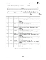
Bits Mnemonic Field
Name
Description
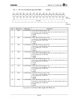
23
RB3E
CHIRXPTRB3EN CHIRXPTRB3EN bit (Initial value: 0, R/W)
This bit is used to enable/disable the timeslot for the receive channel pointed to by
the TDM switch pointer CHIRXPTRB3
0: Disable
1: Enable
22
RB2E
CHIRXPTRB2EN CHIRXPTRB2EN bit (Initial value: 0, R/W)
This bit is used to enable/disable the timeslot for the receive channel pointed to by
the TDM switch pointer CHIRXPTRB2
0: Disable
1: Enable
21
RB1E
CHIRXPTRB1EN CHIRXPTRB1EN bit (Initial value: 0, R/W)
This bit is used to enable/disable the timeslot for the receive channel pointed to by
the TDM switch pointer CHIRXPTRB1
0: Disable
1: Enable
20
RB0E
CHIRXPTRB0EN CHIRXPTRB0EN bit (Initial value: 0, R/W)
This bit is used to enable/disable the timeslot for the receive channel pointed to by
the TDM switch pointer CHIRXPTRB0
0: Disable
1: Enable
19
RA3E
CHIRXPTRA3EN CHIRXPTRA3EN bit (Initial value: 0, R/W)
This bit is used to enable/disable the timeslot for the receive channel pointed to by
the TDM switch pointer CHIRXPTRA3
0: Disable
1: Enable
18
RA2E
CHIRXPTRA2EN CHIRXPTRA2EN bit (Initial value: 0, R/W)
This bit is used to enable/disable the timeslot for the receive channel pointed to by
the TDM switch pointer CHIRXPTRA2
0: Disable
1: Enable
17
RA1E
CHIRXPTRA1EN CHIRXPTRA1EN bit (Initial value: 0, R/W)
This bit is used to enable/disable the timeslot for the receive channel pointed to by
the TDM switch pointer CHIRXPTRA1
0: Disable
1: Enable
16
RA0E
CHIRXPTRA0EN CHIRXPTRA0EN bit (Initial value: 0, R/W)
This bit is used to enable/disable the timeslot for the receive channel pointed to by
the TDM switch pointer CHIRXPTRA0
0: Disable
1: Enable
15:0
⎯
Reserved
⎯
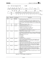
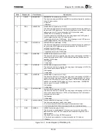
Figure 16.4.2 CHI Pointer Enable Register (PNTREN) (2/2)
Summary of Contents for TMPR4925
Page 1: ...64 Bit TX System RISC TX49 Family TMPR4925 Rev 3 0 ...
Page 4: ......
Page 15: ...Handling Precautions ...
Page 16: ......
Page 18: ...1 Using Toshiba Semiconductors Safely 1 2 ...
Page 40: ...3 General Safety Precautions and Usage Considerations 3 18 ...
Page 42: ...4 Precautions and Usage Considerations 4 2 ...
Page 43: ...TMPR4925 ...
Page 44: ......
Page 54: ...Chapter 1 Features 1 8 ...
Page 58: ...Chapter 2 Block Diagram 2 4 ...
Page 88: ...Chapter 4 Address Mapping 4 12 ...
Page 226: ...Chapter 8 DMA Controller 8 58 ...
Page 260: ...Chapter 9 SDRAM Controller 9 34 ...
Page 480: ...Chapter 15 Interrupt Controller 15 32 ...
Page 554: ...Chapter 19 Real Time Clock RTC 19 8 ...
Page 555: ...Chapter 20 Removed 20 1 20 Removed ...
Page 556: ...Chapter 20 Removed 20 2 ...
Page 564: ...Chapter 21 Extended EJTAG Interface 21 8 ...
Page 580: ...Chapter 22 Electrical Characteristics 22 16 ...
Page 588: ...Chapter 24 Usage Notes 24 2 ...

