Chapter 7 External Bus Controller
7-20
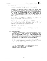
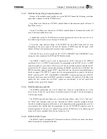
7.3.9 PCMCIA
mode
The EBUSC Controller supports the following functions of the 16-Bit PC Card interface.
The EBUSC Controller supports 2 PCMCIA slots. Any of the eight EBUSC Controller channels can
target the 2 PCMCIA slots. The use of channels 6 and 7 first for PCMCIA is recommended, since their
normal CE_ signals are not pinned out and they cannot be used for any other function. For a channel to
target a PCMCIA slot, it must first be in a PCMCIA mode. This is done by programming the PCM field
to a non zero value. See the PCM field description for more details. Once a channel has been
programmed to a PCMCIA mode, the PCS bit determines which slot is accessed via the two pairs of
Card Enable signals.
Since pin multiplexing exists on the TX4925 device, the PCMCIA pin selection should be configured
appropriately. Please refer to “3.3 Pin Multiplexing” for more information.
It should be noted that a normal dedicated CE_ for a channel used for PCMCIA access will continue
to go active when that channel is accessed. It is up to the system designer to make sure that this does not
cause any conflict on the external buses. The signals BWE*/BE*, OE*, and WE* also continue to cycle
regardless of the PCMCIA mode. This was done for AC timing considerations.
OE* and WE* are forced inactive during IO access.
CARDIORD* and CARDIOWR* are multiplexed on BWE*/BE*[3:2] pins respectively in a time
multiplexed manner on the TX4925.
7.3.9.1
PCMCIA Mode Selects
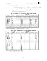
A channel that is allocated to be used as a PCMCIA control channel can be put into one of four
access modes. The first is the Attribute Memory Access mode. This mode is typically used at
power on only to determine the type of PCMCIA card installed. The second is the Common
Memory Access Mode, used for cards that are of the memory type. The third is IO Access mode,
used for cards that support IO. A single channel can be used initially for Attribute access to
determine the card types and then that channel can be reallocated for one of the cards.
In the case of properties access, memory access, and I/O access is determined by differences in
the signals CARDREG*, CARDIORD*, CARDIOWR*, the maximum address space, and width
of the access. Consult the PCMCIA 16-Bit PC Card specification for details.
7.3.9.2
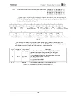
PCMCIA Slot Selection
Slot 1 is accessed by programming the PCS bit to 0 and the CARD1CSH*/CARD1CSL*
signals are active. If the PCS bit is set to 1 then Slot 2 is accessed and the
CARD2CSH*/CARD2CSL* signals are active.
Summary of Contents for TMPR4925
Page 1: ...64 Bit TX System RISC TX49 Family TMPR4925 Rev 3 0 ...
Page 4: ......
Page 15: ...Handling Precautions ...
Page 16: ......
Page 18: ...1 Using Toshiba Semiconductors Safely 1 2 ...
Page 40: ...3 General Safety Precautions and Usage Considerations 3 18 ...
Page 42: ...4 Precautions and Usage Considerations 4 2 ...
Page 43: ...TMPR4925 ...
Page 44: ......
Page 54: ...Chapter 1 Features 1 8 ...
Page 58: ...Chapter 2 Block Diagram 2 4 ...
Page 88: ...Chapter 4 Address Mapping 4 12 ...
Page 226: ...Chapter 8 DMA Controller 8 58 ...
Page 260: ...Chapter 9 SDRAM Controller 9 34 ...
Page 480: ...Chapter 15 Interrupt Controller 15 32 ...
Page 554: ...Chapter 19 Real Time Clock RTC 19 8 ...
Page 555: ...Chapter 20 Removed 20 1 20 Removed ...
Page 556: ...Chapter 20 Removed 20 2 ...
Page 564: ...Chapter 21 Extended EJTAG Interface 21 8 ...
Page 580: ...Chapter 22 Electrical Characteristics 22 16 ...
Page 588: ...Chapter 24 Usage Notes 24 2 ...

