Chapter 3 Signals
3-8
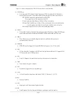
3.1.9
AC-link Interface Signals
Table 3.1.9 AC-link Interface Signals
Signal Name
Type
Description
Initial State
ACRESET
*
Output
AC '97 Master H/W Reset
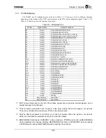
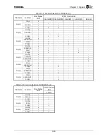
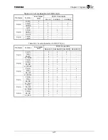
The pin is shared with other functions (refer to Section "3.3 Pin Multiplexing").
PIO input
SYNC
Output
48 kHz Fixed Rate Sample Sync
The pin is shared with other functions (refer to Section "3.3 Pin Multiplexing").
PIO input
SDOUT
Output
Serial, Time Division Multiplexed, AC '97 Output Stream
The pin is shared with other functions (refer to Section "3.3 Pin Multiplexing").
PIO input
SDIN]1]
Input
Serial, Time Division Multiplexed, AC ‘97 Input Stream
The pin is shared with other functions (refer to Section "3.3 Pin Multiplexing").
PIO input
SDIN[0]
Input
Serial, Time Division Multiplexed, AC '97 Input Stream
The pin is shared with other functions (refer to Section "3.3 Pin Multiplexing").
PIO input
BITCLK
Input
12.288 MHz Serial Data Clock
The pin is shared with other functions (refer to Section "3.3 Pin Multiplexing").
PIO input
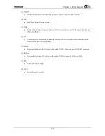
3.1.10 Interrupt
Signals
Table 3.1.10 Interrupt Signals
Signal Name
Type
Description
Initial State
NMI
*
Input
PU
Non-Maskable Interrupt
Non-maskable interrupt signal.
Input
INT[7:0] Input
PU
External Interrupt Requests
External interrupt request signals.
The pins are shared with other functions (refer to Section "3.3 Pin Multiplexing").
PIO input
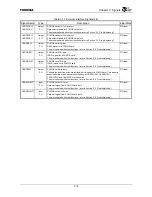
3.1.11 CHI Interface Signals
Table 3.1.11 CHI Interface Signals
Signal Name
Type
Description
Initial State
CHIFS Input/output
PU
CHI Frame synchronization
CHI frame synchronization signal. This pin can be used in either output or input mode.
In output mode, the pin allows the TX4925 to become the master CHI synchronization
source. In input mode, the pin allows the external peripheral device to become the
master CHI synchronization source. In that case, the TX4925 CHI module becomes a
slave for external synchronization.
The pin is shared with other functions (refer to Section "3.3 Pin Multiplexing").
PIO input
CHICLK Input/output
PU
CHI Clock
CHI clock signal. This pin can be used in either output or input mode. In output mode,
the pin allows the TX4925 to become the master CHI clock source. In input mode, the
pin allows the external peripheral device to become the master CHI clock source. In
that case, the TX4925 CHI module becomes a slave for the external clock.
The pin is shared with other functions (refer to Section "3.3 Pin Multiplexing").
PIO input
CHIDOUT Output
PU
CHI Data Output
CHI serial data output signal.
The pin is shared with other functions (refer to Section "3.3 Pin Multiplexing").
PIO input
CHIDIN Input
PU
CHI Data Input
CHI serial data input signal.
The pin is shared with other functions (refer to Section "3.3 Pin Multiplexing").
PIO input
Summary of Contents for TMPR4925
Page 1: ...64 Bit TX System RISC TX49 Family TMPR4925 Rev 3 0 ...
Page 4: ......
Page 15: ...Handling Precautions ...
Page 16: ......
Page 18: ...1 Using Toshiba Semiconductors Safely 1 2 ...
Page 40: ...3 General Safety Precautions and Usage Considerations 3 18 ...
Page 42: ...4 Precautions and Usage Considerations 4 2 ...
Page 43: ...TMPR4925 ...
Page 44: ......
Page 54: ...Chapter 1 Features 1 8 ...
Page 58: ...Chapter 2 Block Diagram 2 4 ...
Page 88: ...Chapter 4 Address Mapping 4 12 ...
Page 226: ...Chapter 8 DMA Controller 8 58 ...
Page 260: ...Chapter 9 SDRAM Controller 9 34 ...
Page 480: ...Chapter 15 Interrupt Controller 15 32 ...
Page 554: ...Chapter 19 Real Time Clock RTC 19 8 ...
Page 555: ...Chapter 20 Removed 20 1 20 Removed ...
Page 556: ...Chapter 20 Removed 20 2 ...
Page 564: ...Chapter 21 Extended EJTAG Interface 21 8 ...
Page 580: ...Chapter 22 Electrical Characteristics 22 16 ...
Page 588: ...Chapter 24 Usage Notes 24 2 ...


