Chapter 4 Address Mapping
4-1
4. Address
Mapping
This chapter explains the physical address map of TX4925.
Please refer to “64-Bit TX System RISC TX49/H2 Core Architecture” about the details of mapping to a
physical address from the virtual address of TX49/H2 core.
4.1
TX4925 Physical Address Map
TX4925 supports up to 4G (2
32
) bytes of physical address.
Following resources are to be allocated in the physical address of the TX4925.
•
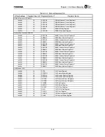
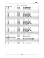
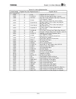
TX4925 Internal registers (refer to “4.2 Register Map”)
•
SDRAM (refer to “9.3.2 Address Mapping”)
•
External Devices such as ROM, I/O Devices (refer to “7.3.3 Address Mapping”)
•
PCI Bus (refer to “10.3.4 Initiator Access”)
Each resource is to be allocated in arbitrary physical addresses by the register setup. Refer to the
explanation of each controller for the details of the mapping.
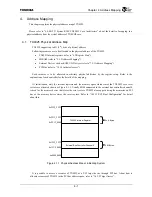
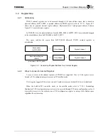
At initialization, only the internal registers and the memory space which stores the TX49/H2 core reset
vectors are allocated shown as Figure 4.1.1. Usually ROM connected to the external bus controller channel 0
is used for the memory device that stores the reset vectors. TX4925 also supports using the memories on PCI
bus as the memory device stores the reset vectors. Refer to “10.3.12 PCI Boot Configuration” for detail
about this.
Figure 4.1.1 Physical Address Map at Initializing System
It is possible to access a resource of TX4925 as a PCI target device through PCI bus. About how to
allocate resources of TX4925 to the PCI bus address space, refer to “10.3.5 Target Access”.
TX4925 Internal Register
External Bus Controller Channel 0
64 K Bytes
0xFFFF_FFFF
0xFF1F_FFFF
0xFF1F_0000
0x1FFF_FFFF
0x1FC0_0000
0x0000_0000
4 M Bytes
Summary of Contents for TMPR4925
Page 1: ...64 Bit TX System RISC TX49 Family TMPR4925 Rev 3 0 ...
Page 4: ......
Page 15: ...Handling Precautions ...
Page 16: ......
Page 18: ...1 Using Toshiba Semiconductors Safely 1 2 ...
Page 40: ...3 General Safety Precautions and Usage Considerations 3 18 ...
Page 42: ...4 Precautions and Usage Considerations 4 2 ...
Page 43: ...TMPR4925 ...
Page 44: ......
Page 54: ...Chapter 1 Features 1 8 ...
Page 58: ...Chapter 2 Block Diagram 2 4 ...
Page 88: ...Chapter 4 Address Mapping 4 12 ...
Page 226: ...Chapter 8 DMA Controller 8 58 ...
Page 260: ...Chapter 9 SDRAM Controller 9 34 ...
Page 480: ...Chapter 15 Interrupt Controller 15 32 ...
Page 554: ...Chapter 19 Real Time Clock RTC 19 8 ...
Page 555: ...Chapter 20 Removed 20 1 20 Removed ...
Page 556: ...Chapter 20 Removed 20 2 ...
Page 564: ...Chapter 21 Extended EJTAG Interface 21 8 ...
Page 580: ...Chapter 22 Electrical Characteristics 22 16 ...
Page 588: ...Chapter 24 Usage Notes 24 2 ...

