Chapter 6 Clocks
6-2
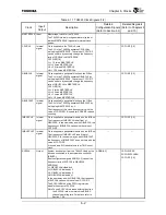
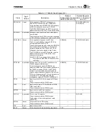
Table 6.1.1 TX4925 Clock Signals (1/2)
Clock
Input/
Output
Description
Related
Configuration Signals
(Refer to Section 3.2)
Related Registers
(Refer to Chapters 5
and 10.)
MASTERCLK Input
Master input clock for the TX4925.
The TX4925 internal clock generator multiplies or
divides MASTERCLK to generate internal clock
pulses.
⎯
⎯
CPUCLK
Internal
signal
Clock supplied to the TX49/H2 core.
The PLL in the TX4925 generates CPUCLK by
multiplying MASTERCLK. The value of CCFG.RF
can be used to dynamically change the frequency
ratio of CPUCLK to MASTERCLK.
CCFG.RF[1:0]
LL = 10 times MASTERCLK
LH = 5 times MASTERCLK
HL = 2.5 times MASTERCLK
HH = 1.25 times MASTERCLK
⎯
CCFG.RF
[1:0]
GBUSCLK
Internal
signal
Clock supplied to peripheral blocks on the G-Bus.
The PLL in the TX4925 generates GBUSCLK by
multiplying MASTERCLK. The value of CCFG.RF
can be used to dynamically change the frequency
ratio of GBUSCLK to MASTERCLK.
CCFG.RF[1:0]
LL = 4 times MASTERCLK
LH = 2 times MASTERCLK
HL = 1 times MASTERCLK
HH = 1/2 times MASTERCLK
⎯
CCFG.RF
[1:0]
GBUSCLKF
Internal
signal
Clock supplied to peripheral blocks on the G-Bus.
The PLL in the TX4925 generates GBUSCLKF by
multiplying MASTERCLK by 4.
The frequency of this clock does not vary with the
value of CCFG.RG. It is used for SDRAMC refresh
counting.
⎯
⎯
IMBUSCLK
Internal
signal
Clock supplied to peripheral modules on the IM-Bus.
The frequency of IMBUSCLK is half that of
GBUSCLK. In the same way as with GBUSCLK, the
frequency of IMBUSCLK varies with the value of
CCFG.RF.
⎯
CCFG.RF
[1:0]
IMBUSCLKF
Internal
signal
Clock supplied to peripheral modules on the IM Bus.
The frequency of IMBUSCLKF is half that of
GBUSCLKF. In the same way as with GBUSCLKF,
the frequency of IMBUSCLKF does not vary with the
value of CCFG.RF.
It is used as a SIO baud rate clock or TMR count
clock.
⎯
⎯
SYSCLK Output
System clock output from the TX4925. Used by the
devices connected to the external bus controller
(EBUSC).
Boot configuration signals ADDR[4: 3] can set the
frequency ratio of SYSCLK to GBUSCLK.
ADDR[4:3]
LL: GBUSCLK divided by 4
LH: GBUSCLK divided by 3
HL: GBUSCLK divided by 2
HH: GBUSCLK divided by 1
In the same way as with GBUSCLK, the frequency
of SYSCLK varies with the value of CCFG.RF.
The SYSCLKEN bit of the PCFG register can
disable the output of SYSCLK.
Note:To use SYSCLK to access external devices,
the SYSCLK rate must match the EBUSC
channel operating rate. For details, refer to
Section 7.3.8.
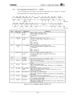
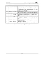
ADDR[4: 3]
CCFG.SYSSP
PCFG.SYSCLKEN
CCFG.RF [1:0]
Summary of Contents for TMPR4925
Page 1: ...64 Bit TX System RISC TX49 Family TMPR4925 Rev 3 0 ...
Page 4: ......
Page 15: ...Handling Precautions ...
Page 16: ......
Page 18: ...1 Using Toshiba Semiconductors Safely 1 2 ...
Page 40: ...3 General Safety Precautions and Usage Considerations 3 18 ...
Page 42: ...4 Precautions and Usage Considerations 4 2 ...
Page 43: ...TMPR4925 ...
Page 44: ......
Page 54: ...Chapter 1 Features 1 8 ...
Page 58: ...Chapter 2 Block Diagram 2 4 ...
Page 88: ...Chapter 4 Address Mapping 4 12 ...
Page 226: ...Chapter 8 DMA Controller 8 58 ...
Page 260: ...Chapter 9 SDRAM Controller 9 34 ...
Page 480: ...Chapter 15 Interrupt Controller 15 32 ...
Page 554: ...Chapter 19 Real Time Clock RTC 19 8 ...
Page 555: ...Chapter 20 Removed 20 1 20 Removed ...
Page 556: ...Chapter 20 Removed 20 2 ...
Page 564: ...Chapter 21 Extended EJTAG Interface 21 8 ...
Page 580: ...Chapter 22 Electrical Characteristics 22 16 ...
Page 588: ...Chapter 24 Usage Notes 24 2 ...

