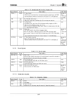
Chapter 3 Signals
3-11
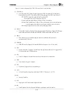
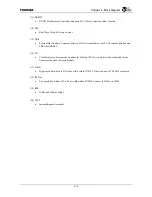
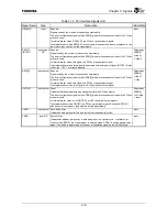
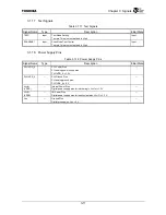
3.1.17 Test
Signals
Table 3.1.17 Test Signals
Signal Name
Type
Description
Initial State
TEST
*
Input
Test Mode Setting
Test pin. This pin must be fixed to High.
Input
SCANENB
*
Input
Scan Mode Test Control
Test pin. This pin must be fixed to High.
Input
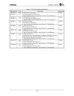
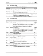
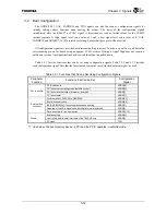
3.1.18 Power
Supply
Pins
Table 3.1.18 Power Supply Pins
Signal Name
Type
Description
Initial State
PLL1VDD_A
⎯
PLL Power Pins
PLL analog power supply pins.
PLL1VDD_A = 1.5 V
⎯
PLL1VSS_A
⎯
PLL
Ground
Pins
PLL analog ground pins.
PLL1VSS_A = 0 V
⎯
VccInt
(VDDC)
⎯
Internal Power Pins
Digital power supply pins for internal logic. VccInt = 1.5 V.
⎯
VccIO
(VDDS)
⎯
I/O Power Pins
Digital power supply pins for input/output pins. VccIO = 3.3 V.
⎯
Vss
⎯
Ground
Pins
Digital ground pins. Vss = 0 V.
⎯
Summary of Contents for TMPR4925
Page 1: ...64 Bit TX System RISC TX49 Family TMPR4925 Rev 3 0 ...
Page 4: ......
Page 15: ...Handling Precautions ...
Page 16: ......
Page 18: ...1 Using Toshiba Semiconductors Safely 1 2 ...
Page 40: ...3 General Safety Precautions and Usage Considerations 3 18 ...
Page 42: ...4 Precautions and Usage Considerations 4 2 ...
Page 43: ...TMPR4925 ...
Page 44: ......
Page 54: ...Chapter 1 Features 1 8 ...
Page 58: ...Chapter 2 Block Diagram 2 4 ...
Page 88: ...Chapter 4 Address Mapping 4 12 ...
Page 226: ...Chapter 8 DMA Controller 8 58 ...
Page 260: ...Chapter 9 SDRAM Controller 9 34 ...
Page 480: ...Chapter 15 Interrupt Controller 15 32 ...
Page 554: ...Chapter 19 Real Time Clock RTC 19 8 ...
Page 555: ...Chapter 20 Removed 20 1 20 Removed ...
Page 556: ...Chapter 20 Removed 20 2 ...
Page 564: ...Chapter 21 Extended EJTAG Interface 21 8 ...
Page 580: ...Chapter 22 Electrical Characteristics 22 16 ...
Page 588: ...Chapter 24 Usage Notes 24 2 ...


