Chapter 9 SDRAM Controller
9-3
9.3 Detailed
Explanation
9.3.1 Supported
SDRAM
Configurations
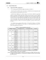
This controller supports the SDRAM Configurations listed below in Table 9.3.1.
The MW field of the SDRAM Channel Control Register (SDCCRn) can be used to separately set the
data bus width for each channel to either 32 bits or 16 bits.
DATA[15:0] and DQM[1:0] are used when using a 16-bit data bus. DQM[3:2] output High.
DATA[31:16] output an undefined value when DATA[15:0] become the output, but enter the High-Z
state when DATA[15:0] are the input. When in the Big Endian Mode, first external access of the upper
half word (bits 31:16) of the internal data bus is performed, then external access of the lower half word
(bits 15:0) is performed. When in the Little Endian Mode, first external access of the lower half word
(bits 15:0) is performed, then external access of the upper half word (bits 31:16) is performed. When
using a 16-bit data bus, two external access will always be performed even when accessing less than 16
bits of data.
The maximum memory capacity per channel when a 32-bit data bus is configured is 512 MBytes
when using 8 512-Mbit SDRAMs with a 4-bit data bus. The total maximum memory capacity is 2
GBytes when totaling up the four channels.
Table 9.3.1 Supported SDRAM Configurations
SDRAM Configuration
Row Address (bit)
Column Address (bit)
Remarks
1 M
×
16
11
8
2 M
×
8
11
9
16 Mbit
2-bank
4 M
×
4
11
10
See Note
2 M
×
32
11
9
2 M
×
32
12
8
4 M
×
16
11
10
4 M
×
16
13
8
8 M
×
8
13
9
2-bank
16 M
×
4
13
10
See Note
2 M
×
32
11
8
4 M
×
16
12
8
8 M
×
8
12
9
64 Mbit
4-bank
16 M
×
4
12
10
See Note
4 M
×
32
12
8
8 M
×
16
12
9
16 M
×
8
12
10
128 Mbit
4-bank
32 M
×
4
12
11
See Note
8 M
×
32
13
8
16 M
×
16
13
9
32 M
×
8
13
10
256 Mbit
4-bank
64 M
×
4
13
11
See Note
32 M
×
16
13
10
64 M
×
8
13
11
512 Mbit
4-bank
128 M
×
4
13
12
See Note
Note1: The SDRAM Controller logic-wise does support these configurations, but please design
carefully since the memory bus load will be large.
Note2: With this composition, since the memory size of one channel is 512 Mbyte, if the memory area
is mapped from physical address 0, it will overlap with the address area which is used for ROM
area of boot vector.
Summary of Contents for TMPR4925
Page 1: ...64 Bit TX System RISC TX49 Family TMPR4925 Rev 3 0 ...
Page 4: ......
Page 15: ...Handling Precautions ...
Page 16: ......
Page 18: ...1 Using Toshiba Semiconductors Safely 1 2 ...
Page 40: ...3 General Safety Precautions and Usage Considerations 3 18 ...
Page 42: ...4 Precautions and Usage Considerations 4 2 ...
Page 43: ...TMPR4925 ...
Page 44: ......
Page 54: ...Chapter 1 Features 1 8 ...
Page 58: ...Chapter 2 Block Diagram 2 4 ...
Page 88: ...Chapter 4 Address Mapping 4 12 ...
Page 226: ...Chapter 8 DMA Controller 8 58 ...
Page 260: ...Chapter 9 SDRAM Controller 9 34 ...
Page 480: ...Chapter 15 Interrupt Controller 15 32 ...
Page 554: ...Chapter 19 Real Time Clock RTC 19 8 ...
Page 555: ...Chapter 20 Removed 20 1 20 Removed ...
Page 556: ...Chapter 20 Removed 20 2 ...
Page 564: ...Chapter 21 Extended EJTAG Interface 21 8 ...
Page 580: ...Chapter 22 Electrical Characteristics 22 16 ...
Page 588: ...Chapter 24 Usage Notes 24 2 ...


