Chapter 8 DMA Controller
8-12
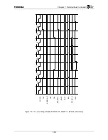
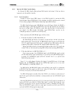
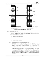
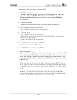
Figure 8.3.3 Dual Address Burst Transfer (DMCCRn.USEXFSZ
=
1)
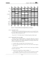
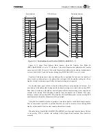
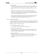
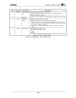
Figure 8.3.4 shows Dual Address Burst transfer when the Transfer Size Mode bit
(DMCCRn.USEXFSZ) is set to “0”, the lower 7 bits of the Transfer Start address for the transfer
source are set to 0x54, the lower 7 bits of the Transfer Start address for the transfer destination are
set to (a) 0x14/(b) 0x18, and the Transfer Setting Size (DMCCRn.XFSZ) is set to 8 words.
Panel (a) of this figure shows when the address offset is equivalent. In this case, first transfer of
three words is performed up to the address that is aligned with the transfer setting size. Then,
transfer of eight words that is specified by the transfer setting size is repeated.
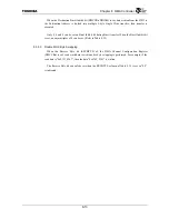
On the other hand, panel (b) show when the address offset is not equivalent. In this case, first
only data up to the address that is aligned with the transfer setting size is read to the on-chip FIFO.
Then, data is written up to the address that is aligned with the transfer setting size as long as data
remains in the on-chip FIFO. Efficiency decreases since the transfer size is divided. Also, since
data may remain in the on-chip FIFO, Burst transfer of a Dual Address that uses the on-chip FIFO
simultaneously with another channel cannot be performed.
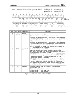
Using the Burst Inhibit bit makes it possible to mix Burst transfer with 8-Word Single transfer.
This in turn makes it possible to perform Burst access only for memory access during DMA
transfer with external I/O devices that cannot perform Burst transfer.
When the Source Burst Inhibit bit (DMCCRn.SBINH) is set, data read from the Source Address
to the on-chip FIFO is divided into multiple 4-byte Single Read transfers, then transfer is
executed.
50
54
58
5c
64
68
6c
60
74
78
7c
70
00
04
08
0c
14
18
1c
10
32
0
10
14
18
1c
24
28
2c
20
34
38
3c
30
40
44
48
4c
54
58
5c
50
32
0
Source Address
FIFO (8 Words)
Destination Address
Summary of Contents for TMPR4925
Page 1: ...64 Bit TX System RISC TX49 Family TMPR4925 Rev 3 0 ...
Page 4: ......
Page 15: ...Handling Precautions ...
Page 16: ......
Page 18: ...1 Using Toshiba Semiconductors Safely 1 2 ...
Page 40: ...3 General Safety Precautions and Usage Considerations 3 18 ...
Page 42: ...4 Precautions and Usage Considerations 4 2 ...
Page 43: ...TMPR4925 ...
Page 44: ......
Page 54: ...Chapter 1 Features 1 8 ...
Page 58: ...Chapter 2 Block Diagram 2 4 ...
Page 88: ...Chapter 4 Address Mapping 4 12 ...
Page 226: ...Chapter 8 DMA Controller 8 58 ...
Page 260: ...Chapter 9 SDRAM Controller 9 34 ...
Page 480: ...Chapter 15 Interrupt Controller 15 32 ...
Page 554: ...Chapter 19 Real Time Clock RTC 19 8 ...
Page 555: ...Chapter 20 Removed 20 1 20 Removed ...
Page 556: ...Chapter 20 Removed 20 2 ...
Page 564: ...Chapter 21 Extended EJTAG Interface 21 8 ...
Page 580: ...Chapter 22 Electrical Characteristics 22 16 ...
Page 588: ...Chapter 24 Usage Notes 24 2 ...

