


ML62Q1000 Series User's Manual
Chapter 29 Safety Function
FEUL62Q1000
29-13
29.3 Description of Operation
29.3.1 Communication Function Self-Test
This self test is enabled by the COMFT0 register setting.
The communication function can be tested through the self test by internally connecting transmit and receive data of
UART and SSIO (synchronous serial port) of the serial communication unit.
Before testing the communication, write "1" to the corresponding bit of the COMFT0 register.
Transmit side data output can be enabled/disabled by setting the mode (secondary to octonary function) of the
general-purpose port.
For receive side data, it is not required to set the mode (2
nd
to 8
th
function) of the general-purpose port.
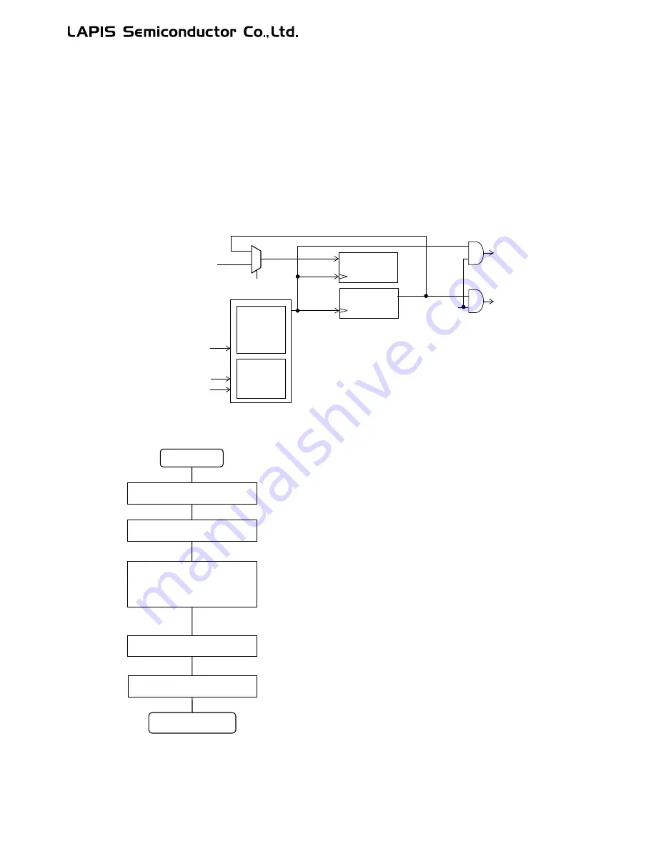
Figure 29-1 shows a concept diagram of the communication test. Figure 29-2 shows a flow chart of the communication
test.
Figure 29-1 Communication Test Concept Diagram
Figure 29-2 Communication Test Flow Chart
Receive
register
HSCLK
LSCLK
RXDn
SINn
SCKn
TXDn
SOUTn
Clock selection
&
frequency
division circuit
Baud rate
generator
SCLKn
Transmit
register
COMFT0
PnMOD0 to 7
PnMOD0 to 7: Port n mode register
Write "1" to the corresponding bit to enable the communication
test function.
To output the transmit data from the general-purpose port, set the
communication mode (2
nd
to 8
th
function). When not output, set to
the primary function.
Start setting
Set the function (UART/SSIO) to be tested for communication to
the transmit/receive mode. Start transmission/reception.
For details, see the chapter describing each function.
End
Transmit operation ended
Set transmit/receive mode,
transmit data, and
transmission/reception start
Set general-purpose port
Set COMFT0 register
Read the received data and compare it with the transmit data.
Check received data
Write "0" to the corresponding bit to disable the communication
test function.
Reset COMFT0 register
Summary of Contents for ML62Q1000 Series
Page 17: ...Chapter 1 Overview...
Page 112: ...Chapter 2 CPU and Memory Space...
Page 154: ...Chapter 3 Reset Function...
Page 166: ...Chapter 4 Power Management...
Page 196: ...Chapter 5 Interrupts...
Page 248: ...Chapter 6 Clock generation Circuit...
Page 274: ...Chapter 7 Low Speed Time Base Counter...
Page 291: ...Chapter 8 16 Bit Timer...
Page 320: ...Chapter 9 Functional Timer FTM...
Page 382: ...Chapter 10 Watchdog Timer...
Page 402: ...Chapter 11 Serial Communication Unit...
Page 456: ...Chapter 12 I2 C Bus Unit...
Page 491: ...Chapter 13 I2 C Master...
Page 512: ...Chapter 14 DMA Controller...
Page 531: ...Chapter 15 Buzzer...
Page 550: ...Chapter 16 Simplified RTC...
Page 559: ...Chapter 17 GPIO...
Page 594: ...Chapter 18 External Interrupt Function...
Page 612: ...Chapter 19 CRC Generator...
Page 632: ...Chapter 20 Analog Comparator...
Page 644: ...Chapter 21 D A Converter...
Page 655: ...Chapter 22 Voltage Level Supervisor...
Page 676: ...Chapter 23 Successive Approximation Type A D Converter...
Page 709: ...Chapter 24 Regulator...
Page 714: ...Chapter 25 Flash Memory...
Page 743: ...Chapter 26 Code Option...
Page 750: ...Chapter 27 LCD Driver...
Page 788: ...Chapter 28 On Chip Debug Function...
Page 795: ...Chapter 29 Safety Function...
Page 813: ...Appendix A...
Page 881: ...Revision History...