


ML62Q1000 Series User's Manual
Chapter 11 Serial Communication Unit
FEUL62Q1000
11-49
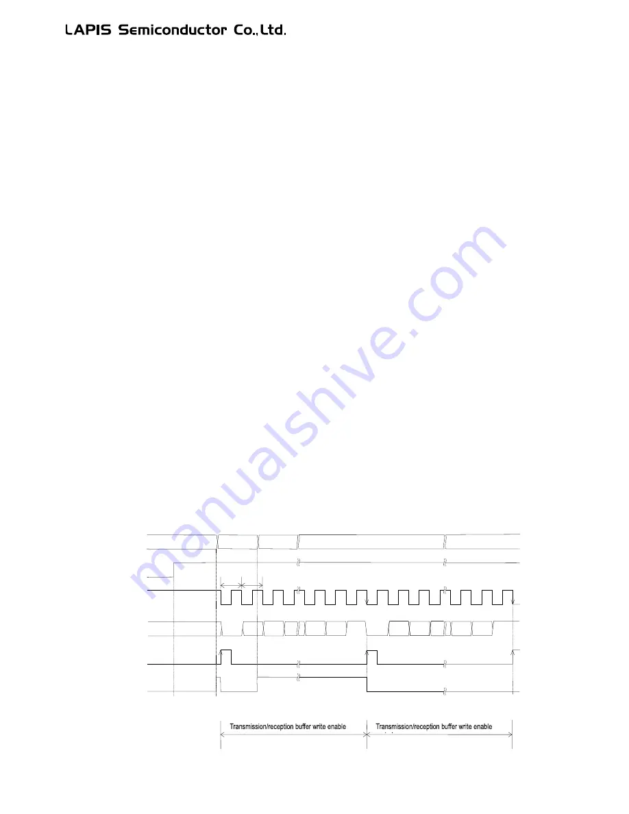
11.3.2.4 Transmit Operation
The following shows the transmission procedure in the UART full-duplex communication mode. Figure 11-15 shows the
operation timing for transmission.
Ÿ
To prepare the communication (settings common to transmission/reception for full-duplex communication):
−
Choose the full-duplex communication mode in the serial communication unit n mode register (SUnMOD).
−
If using the transmission interval function, set the serial communication unit n transmission interval setting
register (SUnDLYL).
−
Choose the communication mode with the UARTn0 mode register (UAn0MOD).
−
Set the baud rate with the UARTn0 baud rate register (UAn0BRT) and the UARTn0 baud rate adjustment
register (UAn0BRC).
−
Set the shared function for the general-purpose port to use for UART communication, then choose the pin
mode.
−
Clear the request bit for the serial communication unit n0 and n1 interrupts. (QSIUn0=0, QSIUn1=0)
−
Enable the serial communication unit n0 and n1 interrupts. (ESIUn0=1, ESIUn1=1)
−
Read the serial communication unit n transmission/reception buffer L (SDnBUFL) to prevent a false detection
of overrun errors. The read data can be discarded.
−
Write "0xFF" to the UARTn0 status register (UAn0STAT) to clear each flags.
Ÿ
To start transmission:
−
Enable transmission/reception by setting Un0EN bit of the serial communication unit n control register
(SUnCONL) to "1". (1)
−
Writing transmission data to the serial communication unit n transmission/reception buffer H (SDnBUFH) (2)
causes Un0FUL of UAn0STAT to be set to "1" and the baud rate generator to generate the internal transfer
clock. Then the transmission is started.
−
Once the the transmission is started, the start bit is output to the SUn_TXD1 pin at the falling edge of the
internal transfer clock. Un0FUL simultaneously becomes "0". (3)
−
Then, the serial communication unit n1 interrupt (SIUn1INT) is generated if generation of interrupts at the
start and end of the data transmission is chosen in the serial communication unit n mode register (SUnMOD).
Ÿ
Continuous transmission
−
Write the next transmission data into the SDnBUFH register after checking the Un0FUL bit gets "0" by the
previous transmission and the serial communication unit n1 interrupt(SIUn1INT) has occurred (4). This
writing causes the Un0FUL register to be set to "1". Writing subsequently transmission data within the
transmission/reception buffer write enable period (5) makes it possible to transmission data continuously.
−
Once the transmission of the stop bit of the first transmitted data is completed (6), the transmission is
continued if the Un0FUL register is set to "1" and the serial communication unit n1 interrupt (SIUn1INT) is
simultaneously generated.
Ÿ
Transmission end
−
When the transmission is completed without writing the subsequently transmitted data (7), the transmission is
stopped and the serial communication unit n1 interrupt (SIUn1INT) is simultaneously generated.
−
If continuing the transmission, write the transmission data to SDnBUFH. To stop all the UART
transmission/reception, reset the Un0EN bit of the SUnCONL to "0".
Figure 11-15 Operation Timing in Transmission
2nd data
1st data
SDnBUFH
Un0E
Internal
transfer
clock
SUn_TXD1
SIUn1INT
Un0FUL
BRT
BRT
Start
0
1
2
7
Parity
Stop
Start
0
1
2
7
Parity
Stop
↑
(1)
↑
(2)
↑
(3)
↑
(4)
↑
(6)
(5)
(5)
↑
(7)
Summary of Contents for ML62Q1000 Series
Page 17: ...Chapter 1 Overview...
Page 112: ...Chapter 2 CPU and Memory Space...
Page 154: ...Chapter 3 Reset Function...
Page 166: ...Chapter 4 Power Management...
Page 196: ...Chapter 5 Interrupts...
Page 248: ...Chapter 6 Clock generation Circuit...
Page 274: ...Chapter 7 Low Speed Time Base Counter...
Page 291: ...Chapter 8 16 Bit Timer...
Page 320: ...Chapter 9 Functional Timer FTM...
Page 382: ...Chapter 10 Watchdog Timer...
Page 402: ...Chapter 11 Serial Communication Unit...
Page 456: ...Chapter 12 I2 C Bus Unit...
Page 491: ...Chapter 13 I2 C Master...
Page 512: ...Chapter 14 DMA Controller...
Page 531: ...Chapter 15 Buzzer...
Page 550: ...Chapter 16 Simplified RTC...
Page 559: ...Chapter 17 GPIO...
Page 594: ...Chapter 18 External Interrupt Function...
Page 612: ...Chapter 19 CRC Generator...
Page 632: ...Chapter 20 Analog Comparator...
Page 644: ...Chapter 21 D A Converter...
Page 655: ...Chapter 22 Voltage Level Supervisor...
Page 676: ...Chapter 23 Successive Approximation Type A D Converter...
Page 709: ...Chapter 24 Regulator...
Page 714: ...Chapter 25 Flash Memory...
Page 743: ...Chapter 26 Code Option...
Page 750: ...Chapter 27 LCD Driver...
Page 788: ...Chapter 28 On Chip Debug Function...
Page 795: ...Chapter 29 Safety Function...
Page 813: ...Appendix A...
Page 881: ...Revision History...