X20 system modules • Other functions • X20PS4951
X20 system User's Manual 3.10
2329
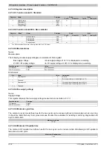
4.26.10.8 Register description
4.26.10.8.1 Function model 0 - Standard
Read
Write
Register
Name
Data type
Cyclic
Non-cyclic
Cyclic
Non-cyclic
USINT
ShortCircuit01
Bit 0
...
...
ShortCircuit01
Bit 3
OpenLine01
Bit 4
...
...
0
OpenLine04
Bit 7
●
4.26.10.8.2 Function model 254 - Bus controller
Read
Write
Register
Offset
1)
Name
Data type
Cyclic
Non-cyclic
Cyclic
Non-cyclic
USINT
ShortCircuit01
Bit 0
...
...
ShortCircuit01
Bit 3
OpenLine01
Bit 4
...
...
0
0
OpenLine04
Bit 7
●
1)
The offset specifies the position of the register within the CAN object.
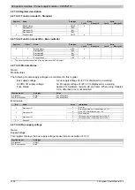
4.26.10.8.3 Supply status
Name:
OpenLine01 to OpenLine04
ShortCircuit01 to ShortCircuit04
This register can be used to display the status of the respective channels.
Data type
Value
USINT
See bit structure.
Bit structure:
Bit
Name
Value
Information
0
No short circuit
0
ShortCircuit01
1
Short circuit on channel 1
...
...
0
No short circuit
3
ShortCircuit04
1
Short circuit on channel 4
0
No open line
4
OpenLine01
1
Open line on channel 1
...
...
0
No open line
7
OpenLine04
1
Open line on channel 4
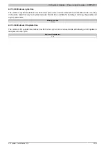
4.26.10.8.4 Minimum cycle time
The minimum cycle time defines how far the bus cycle can be reduced without communication errors occurring.
It should be noted that very fast cycles decrease the idle time available for handling monitoring, diagnostics and
acyclic commands.
Minimum cycle time
100 μs
4.26.10.8.5 Minimum I/O update time
The minimum I/O update time defines how far the bus cycle can be reduced while still allowing an I/O update to
take place in each cycle.
Minimum I/O update time
1 ms
Summary of Contents for X20 System
Page 2: ......


