background image

Intel

®

 IXP45X and Intel

®

 IXP46X Product Line of Network Processors

August 2006

Developer’s Manual

Order Number: 306262-004US

885

I2C Bus Interface Unit—Intel

®

 IXP45X and Intel

®

 IXP46X Product Line of Network Processors

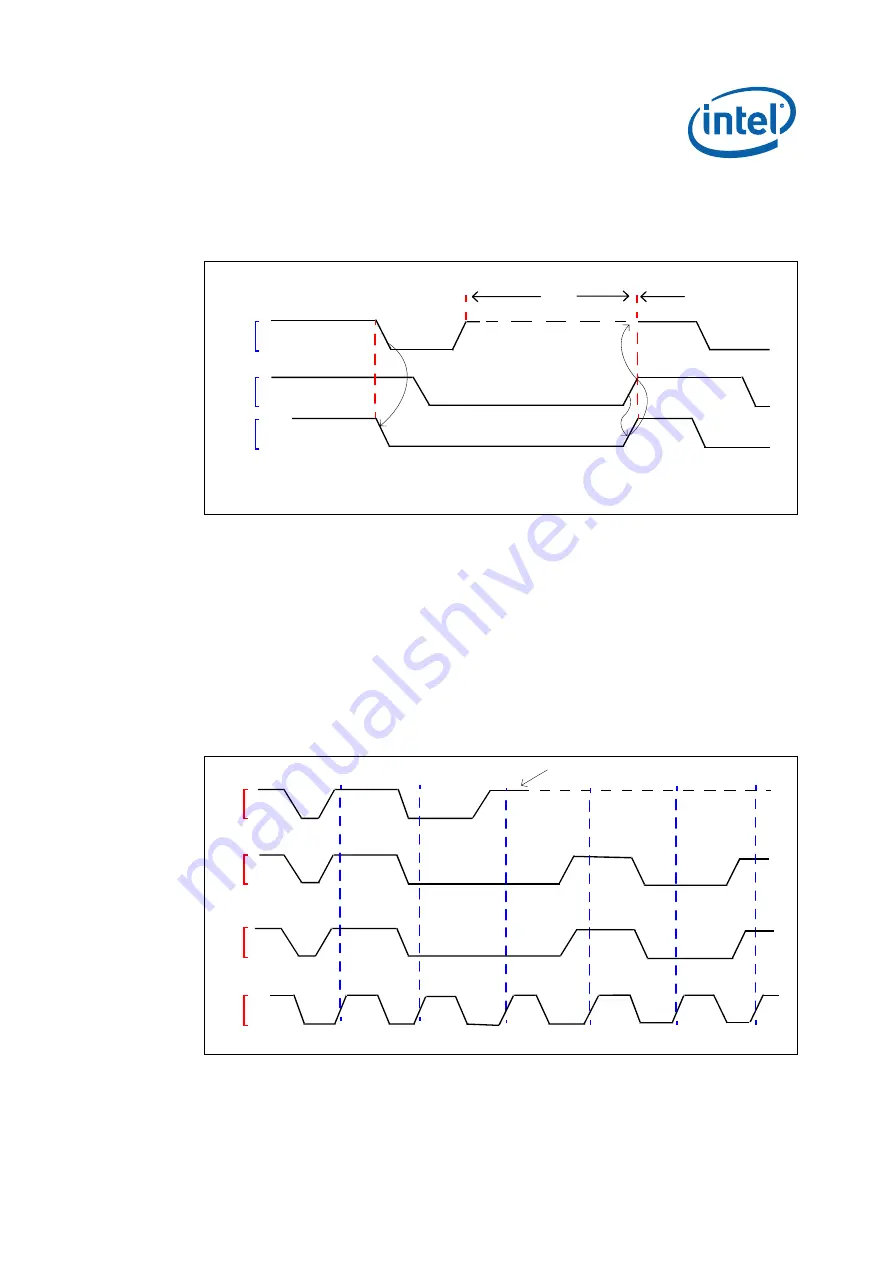
SCL line. Masters with shorter periods are held in a high wait-state during this time. 

Once the master with the longest period completes, the SCL line transitions to the high 

state, masters with the shorter periods can continue the data cycle.

21.5.4.2

SDA Arbitration

Arbitration on the SDA line can continue for a long period starting with the address and 

R/W# bits and continuing with the data bits. 

Figure 197

 shows the arbitration 

procedure for two masters (more than two may be involved depending on how many 

masters are connected to the bus). When the address bit and the R/W# are the same, 

the arbitration is then handled by the logic level of the data that is being driven. Due to 

the wired-AND nature of the I

2

C bus, no data is lost when both (or all) masters are 

outputting the same bus states. When the address, R/W# bit, or data is different, the 

master that output the first high data bit loses arbitration and shuts its data drivers off. 

When the I

2

C unit loses arbitration, it shuts off the SDA or SCL drivers for the 

remainder of the byte transfer, sets the arbitration loss detected ISR bit, then returns 

to idle (Slave-Receive) mode. 

Figure 196. Clock Synchronization During the Arbitration Procedure

B4261-01

CLK2

SCL

Wait

State 

Start Counting 

High Period 

CLK1

The first master to complete its high 

period pulls the 

SCL

 line low.

The master with the longest clock 

period holds the 

SCL

 line low.

Figure 197. Arbitration Procedure of Two Masters

B4262-01

SDA

SCL

Data 1

Data 2

Transmitter 1 Leaves Arbitration 

Data 1 SDA

Summary of Contents for IXP45X

Page 1: ...Order Number 306262 004US Intel IXP45X and Intel IXP46X Product Line of Network Processors Developer s Manual August 2006 ...

Page 2: ...pplications Intel may make changes to specifications and product descriptions at any time without notice Intel may make changes to specifications and product descriptions at any time without notice Designers must not rely on the absence or characteristics of any features or instructions marked reserved or undefined Intel reserves these for future definition and shall have no responsibility whatsoe...

Page 3: ... USB Interfaces 52 2 1 5 1 USB 1 1 Device Interface 52 2 1 5 2 USB 2 0 Host Interface 52 2 1 6 PCI Controller 52 2 1 7 DDRI SDRAM Controller 53 2 1 8 Expansion Interface 54 2 1 9 High Speed Serial Interfaces 56 2 1 10 UARTs 56 2 1 11 GPIO 56 2 1 12 Internal Bus Performance Monitoring Unit IBPMU 57 2 1 13 Interrupt Controller 57 2 1 14 Timers 58 2 1 15 IEEE 1588 Hardware Assist 58 2 1 16 Synchronou...

Page 4: ...che Type Registers 98 3 5 1 2 Register 1 Control and Auxiliary Control Registers 100 3 5 1 3 Register 2 Translation Table Base Register 102 3 5 1 4 Register 3 Domain Access Control Register 102 3 5 1 5 Register 4 Reserved 102 3 5 1 6 Register 5 Fault Status Register 102 3 5 1 7 Register 6 Fault Address Register 103 3 5 1 8 Register 7 Cache Functions 103 3 5 1 9 Register 8 TLB Operations 104 3 5 1 ...

Page 5: ...fer 132 3 6 12 1 Trace Buffer CP Registers 132 3 6 13 Trace Buffer Entries 134 3 6 13 1 Message Byte 134 3 6 13 2 Trace Buffer Usage 137 3 6 14 Downloading Code in ICache 139 3 6 14 1 LDIC JTAG Command 139 3 6 14 2 LDIC JTAG Data Register 140 3 6 14 3 LDIC Cache Functions 141 3 6 14 4 Loading IC During Reset 142 3 6 14 5 Dynamically Loading IC After Reset 147 3 6 14 6 Mini Instruction Cache Overvi...

Page 6: ...truction Timings 184 3 9 4 4 Multiply Instruction Timings 185 3 9 4 5 Saturated Arithmetic Instructions 187 3 9 4 6 Status Register Access Instructions 187 3 9 4 7 Load Store Instructions 187 3 9 4 8 Semaphore Instructions 188 3 9 4 9 Coprocessor Instructions 188 3 9 4 10 Miscellaneous Instruction Timing 189 3 9 4 11 Thumb Instructions 189 3 10 Optimization Guide 189 3 10 1 Introduction 189 3 10 1...

Page 7: ...Frames with MII Interfaces 236 6 1 6 General Ethernet Coprocessor Configuration 238 6 2 Register Descriptions Ethernet MACs 239 6 2 1 Ethernet MAC 0 on NPE B 240 6 2 2 Ethernet MAC 1 on NPE B 241 6 2 3 Ethernet MAC 2 on NPE B 243 6 2 4 Ethernet MAC 2 on NPE B 244 6 2 5 Ethernet MAC on NPE A 246 6 2 6 Ethernet MAC on NPE C 247 6 2 7 Transmit Control 1 249 6 2 8 Transmit Control 2 249 6 2 9 Receive ...

Page 8: ...OPIA Transmit Module 269 7 3 UTOPIA Receive Module 272 7 4 UTOPIA Level 2 Coprocessor NPE Coprocessor Bus Interface 275 7 5 MPHY Polling Routines 275 7 6 UTOPIA Level 2 Clocks 276 8 0 USB 1 1 Device Controller 278 8 1 USB Overview 278 8 2 Device Configuration 279 8 3 USB Operation 280 8 3 1 Signalling Levels 280 8 3 2 Bit Encoding 281 8 3 3 Field Formats 282 8 3 4 Packet Formats 283 8 3 4 1 Token ...

Page 9: ...UDC Endpoint 2 Control Status Register 298 8 5 4 1 Receive FIFO Service RFS 298 8 5 4 2 Receive Packet Complete RPC 298 8 5 4 3 Bit 2 Reserved 298 8 5 4 4 Bit 2 Reserved 298 8 5 4 5 Sent Stall SST 299 8 5 4 6 Force Stall FST 299 8 5 4 7 Receive FIFO Not Empty RNE 299 8 5 4 8 Receive Short Packet RSP 299 8 5 5 UDC Endpoint 3 Control Status Register 300 8 5 5 1 Transmit FIFO Service TFS 300 8 5 5 2 ...

Page 10: ...8 5 10 6 Bit 5 Reserved 312 8 5 10 7 Bit 6 Reserved 312 8 5 10 8 Transmit Short Packet TSP 312 8 5 11 UDC Endpoint 9 Control Status Register 313 8 5 11 1 Receive FIFO Service RFS 313 8 5 11 2 Receive Packet Complete RPC 313 8 5 11 3 Receive Overflow ROF 313 8 5 11 4 Bit 3 Reserved 313 8 5 11 5 Bit 4 Reserved 314 8 5 11 6 Bit 5 Reserved 314 8 5 11 7 Receive FIFO Not Empty RNE 314 8 5 11 8 Receive S...

Page 11: ...T 326 8 5 17 6 Force STALL FST 326 8 5 17 7 Bit 6 Reserved 327 8 5 17 8 Transmit Short Packet TSP 327 8 5 18 UDC Interrupt Control Register 0 328 8 5 18 1 Interrupt Mask Endpoint x IMx where x is 0 through 7 328 8 5 19 UDC Interrupt Control Register 1 329 8 5 19 1 Interrupt Mask Endpoint x IMx where x is 8 through 15 329 8 5 20 UDC Status Interrupt Register 0 330 8 5 20 1 Endpoint 0 Interrupt Requ...

Page 12: ...ister 2 343 8 5 33 UDC Data Register 3 343 8 5 34 UDC Data Register 4 344 8 5 35 UDC Data Register 5 345 8 5 36 UDC Data Register 6 345 8 5 37 UDC Data Register 7 346 8 5 38 UDC Data Register 8 346 8 5 39 UDC Data Register 9 347 8 5 40 UDC Data Register 10 348 8 5 41 UDC Data Register 11 348 8 5 42 UDC Data Register 12 349 8 5 43 UDC Data Register 13 349 8 5 44 UDC Data Register 14 350 8 5 45 UDC ...

Page 13: ...uctures 387 9 13 1 Periodic Frame List 388 9 13 2 Asynchronous List Queue Head Pointer 390 9 13 3 Isochronous High Speed Transfer Descriptor iTD 391 9 13 3 1 Next Link Pointer 392 9 13 3 2 iTD Transaction Status and Control List 393 9 13 3 3 iTD Buffer Page Pointer List Plus 394 9 13 4 Split Transaction Isochronous Transfer Descriptor siTD 395 9 13 4 1 Next Link Pointer 395 9 13 4 2 siTD Endpoint ...

Page 14: ...r 439 9 14 9 1 Nak Count Reload Control 440 9 14 10Managing Control Bulk Interrupt Transfers via Queue Heads 441 9 14 10 1Fetch Queue Head 443 9 14 10 2Advance Queue 443 9 14 10 3Execute Transaction 444 9 14 10 4Write Back qTD 449 9 14 10 5Follow Queue Head Horizontal Pointer 449 9 14 10 6Buffer Pointer List Use for Data Streaming with qTDs 449 9 14 10 7Adding Interrupt Queue Heads to the Periodic...

Page 15: ...ed Type 0 Write Transaction 513 10 2 7 3 Initiated Type 1 Read Transaction 514 10 2 7 4 Initiated Type 1 Write Transaction 515 10 2 7 5 Initiated Memory Read Transaction 516 10 2 7 6 Initiated Memory Write Transaction 517 10 2 7 7 Initiated I O Read Transaction 517 10 2 7 8 Initiated I O Write Transaction 518 10 2 7 9 Initiated Burst Memory Read Transaction 519 10 2 7 10Initiated Burst Memory Writ...

Page 16: ...ter 562 10 5 3 7 PCI Controller Configuration Port Read Data Register 562 10 5 3 8 PCI Controller Control and Status Register 563 10 5 3 9 PCI Controller Interrupt Status Register 564 10 5 3 10PCI Controller Interrupt Enable Register 565 10 5 3 11DMA Control Register 565 10 5 3 12AHB Memory Base Address Register 566 10 5 3 13AHB I O Base Address Register 567 10 5 3 14PCI Memory Base Address Regist...

Page 17: ... 3 ECC Checking 620 11 2 3 4 Scrubbing 624 11 2 3 5 ECC Disabled 625 11 2 3 6 ECC Testing 625 11 2 4 Overlapping Memory Regions 626 11 2 5 DDRI SDRAM Clocking 626 11 2 6 Performance Monitoring 626 11 3 Power Failure Mode 627 11 4 Interrupts Error Conditions 627 11 4 1 Single Bit Error Detection 628 11 4 2 Multi Bit Error Detection 629 11 5 Reset Conditions 629 11 6 Register Definitions 630 11 6 1 ...

Page 18: ... 695 12 4 5 8 Back to Back 1 Word Reads without EX_SLAVE_CS_N Deasserted 696 12 4 5 9 Eight Word Inbound Read 696 12 4 5 10Eight Word Inbound Read with Master Wait States 697 12 4 5 11Eight Word Inbound Read with Deassertion of EX_SLAVE_CS_N 698 12 4 6 Expansion Bus Arbiter Timing Diagrams 698 12 4 6 1 Arbitration When GrantRemove Bit In EXP_MST_CONTROL is Set 698 12 4 6 2 Arbitration When GrantRe...

Page 19: ...ted Framing Protocols 736 13 5 1 T1 736 13 5 2 E1 738 13 5 3 GCI 740 13 5 3 1 Line Card Mode 740 13 5 3 2 Termination Mode 741 13 5 4 MVIP 742 13 5 4 1 2 048 Mbps Backplane 743 13 5 4 2 4 096 Mbps Backplane 744 13 5 4 3 8 192 Mbps Backplane 746 14 0 Universal Asynchronous Receiver Transmitter UART 749 14 1 Overview 749 14 2 Feature List 750 14 3 Block Diagram 751 14 4 Theory of Operation 752 14 4 ...

Page 20: ...Event Counters 788 16 3 2 Occurrence Events 788 16 3 3 Duration Events 789 16 3 4 Performance Monitoring 791 16 3 4 1 Halt Performance Monitoring Disabled 791 16 3 4 2 Cycle Count 791 16 3 4 3 MCU DRAM Transactions 791 16 3 4 4 Events 792 16 4 Previous Master and Slave 792 16 5 Miscellaneous 792 16 5 1 Interrupts 792 16 5 2 Reset Conditions 793 16 6 Detailed Register Descriptions 793 16 6 1 Event ...

Page 21: ...5 18 5 9 Timer Status 826 18 5 10Timestamp Compare Register 826 18 5 11Timestamp Configuration Register 827 18 5 12Timestamp Prescale Register 827 18 5 13General Purpose Timer 0 Configuration Register 828 18 5 14General Purpose Timer 0 Prescale Register 828 18 5 15General Purpose Timer 1 Configuration Register 829 18 5 16General Purpose Timer 1 Prescale Register 829 19 0 Time Synchronization Hardw...

Page 22: ...equenceID SourceUUID_High Register Per Channel 855 20 0 Synchronous Serial Port 857 20 1 SSP Operation 857 20 1 1 Processor Initiated Data Transfer 857 20 2 Data Formats 858 20 2 1 Serial Data Formats for Transfer to from Peripherals 858 20 2 1 1 SSP Format Detail 859 20 2 1 2 SPI Format Detail 859 20 2 1 3 Microwire Format Details 861 20 2 2 Parallel Data Formats for Buffer Storage 862 20 3 Buffe...

Page 23: ...Line SCL Generation 881 21 5 2 Data and Addressing Management 882 21 5 2 1 Addressing a Slave Device 882 21 5 3 I2 C Acknowledge 883 21 5 4 Arbitration 884 21 5 4 1 SCL Arbitration 884 21 5 4 2 SDA Arbitration 885 21 5 5 Master Operations 886 21 5 6 Slave Operations 889 21 5 7 General Call Address 891 21 6 Slave Mode Programming Examples 892 21 6 1 Initialize Unit 892 21 6 2 Write n Bytes as a Sla...

Page 24: ...25 4 3 EAU Count Register 917 25 4 4 EAU Interrupt Register 918 25 4 5 EAU RAM Registers 918 25 5 Performance Requirements 919 26 0 Hashing Unit SHA 921 26 1 Overview 921 26 2 Feature List 921 26 3 Block Diagram 921 26 4 Detailed Register Descriptions 921 26 4 1 Hash Configuration Register 922 26 4 2 Hash Do Register 922 26 4 3 Hash Interrupt Register 923 26 4 4 Hash Chain Register 923 26 4 5 Hash...

Page 25: ...plemented Addresses 951 28 1 1 2 Illegal Access Types 951 28 1 1 3 Expansion Bus Parity Error 951 28 1 1 4 AQM Parity Error 951 28 1 1 5 Memory Controller Unit MCU Multiple Bit ECC Error 951 28 2 Responses to Errors 952 28 2 1 PCI Responses to Errors 952 28 2 2 NPE Responses to Errors 952 28 2 3 Expansion Bus Controller Response to Errors 957 28 2 4 Intel XScale Processor Response to Errors 957 28...

Page 26: ...Queue Head Structure Layout 404 51 Frame Span Traversal Node Structure Layout 408 52 Example USB 2 0 Host Controller Port Routing Block Diagram 411 53 Port Owner Hand Off State Machine 414 54 Derivation of Pointer into Frame List Array 419 55 General Format of Asynchronous Schedule List 419 56 Best Fit Approximation 421 57 Frame Boundary Relationship between HS bus and FS LS Bus 423 58 Relationshi...

Page 27: ...99 Byte Lane Routing During DMA Transfers 546 100 Byte Lane Routing During CSR Accesses 547 101 Memory Controller Block Diagram 584 102 Dual Bank DDRI SDRAM Memory Subsystem 589 103 64 Bit to 32 Bit Addressing 594 104 Page Hit Miss Logic for 128 256 512 1 024 Bit Mode 596 105 Logical Memory Image of a DDRI SDRAM Memory Subsystem 597 106 Supported DDRI SDRAM Extended Mode Register Settings 599 107 ...

Page 28: ...Inbound Write with NOPS 693 155 Eight Word Inbound Write with EX_SLAVE_CS_N Deassertion 694 156 Back to Back 1 Word Inbound Reads with EX_SLAVE_CS_N 695 157 Back to Back 1 Word Reads without EX_SLAVE_CS_N Deasserted 696 158 Eight Word Inbound Read 696 159 Eight Word Inbound Read with Master Wait States 697 160 Eight Word Inbound Read with Deassertion of EX_SLAVE_CS_N 698 161 Arbitration When Grant...

Page 29: ...to Slave Receiver 891 202 Master Receiver Read to Slave Transmitter 891 203 Master Receiver Read to Slave Transmitter Repeated START Master Transmitter Write to Slave Receiver 891 204 General Call Address 892 205 AHB PKE Bridge Block Diagram 908 206 Exponentiation Acceleration Unit Block Diagram 914 207 AHB Queue Manager 927 208 Representative Logical Diagram of a Queue 931 209 NPE Error Handling ...

Page 30: ...egister Summary 133 49 Checkpoint Register CHKPTx 133 50 TBREG Format 134 51 Message Byte Formats 135 52 LDIC Cache Functions 141 53 Debug Handler Code to Implement Synchronization During Dynamic Code Download 149 54 Debug Handler Code Download Bit and Overflow Flag 155 55 Performance Monitoring Registers 157 56 Register Legend 158 57 Clock Count Register CCNT 158 58 Performance Monitor Count Regi...

Page 31: ...p 226 100 Register Legend 240 101 Ethernet MAC 0 on NPE B 240 102 Ethernet MAC 1 on NPE B 241 103 Ethernet MAC 2 on NPE B 243 104 Ethernet MAC 2 on NPE B 244 105 Ethernet MAC on NPE A 246 106 Ethernet MAC on NPE C 247 107 Endpoint Configuration Universal Serial Bus Device Controller 280 108 USB States 281 109 Endpoint Field Addressing 283 110 IN OUT and SETUP Token Packet Format 284 111 SOF Token ...

Page 32: ... 162 Endpoint Capabilities Queue Head DWord 2 406 163 Current qTD Link Pointer 407 164 Host Controller Rules for Bits in Overlay DWords 5 6 8 and 9 408 165 FSTN Normal Path Pointer Signals 409 166 FSTN Back Path Link Pointer Signals 409 167 Default Values of Operational Register Space 410 168 Default Port Routing Depending on EHCI HC CF Bit 412 169 Port Power Enable Control Rules 415 170 Behavior ...

Page 33: ...AM Commands 598 212 Typical Refresh Frequency Register Values 614 213 Syndrome Decoding 620 214 MCU Error Response 627 215 Register Legend 630 216 Memory Controller Register Table 630 217 Example Expansion Bus Pin Mappings to Target Devices 651 218 Supported AHB Commands 652 219 Trimmed Version of IXP45X IXP46X network processors Memory Map 653 220 Expansion Bus Address and Data Byte Steering 656 ...

Page 34: ...k Rates 834 267 Register Legend 836 268 Register Summary Table 837 269 Register Summary 838 270 Texas Instruments Synchronous Serial Frame Format 859 271 Motorola SPI Frame Format 861 272 National Microwire Frame Format 862 273 SSP Serial Port Register Summary 863 274 Register Legend 864 275 Motorola SPI Frame Formats for SPO and SPH Programming 867 276 I2 C Bus Definitions 876 277 Modes of Operat...

Page 35: ...6X Product Line of Network Processors August 2006 Developer s Manual Order Number 306262 004US 35 Contents Intel IXP45X and Intel IXP46X Product Line of Network Processors 299 NPE Coprocessor Response 955 300 NPE Reset State 956 ...

Page 36: ...03 Section 2 2 11 Corrected number of PMU 32 bit event counters to 4 SCR4324 Figure 33 and Figure 34 Corrected UTP_OP_ADDR and UTP_IP_ADDR values in UTOPIA polling illustrations SCR4323 Section 11 2 3 5 Clarified MCU behavior when ECC disabled SCR4303 Section 12 4 1 5 Added new description and figures for using I O wait Table 99 and Section 17 4 Corrected multiple text references for NPE A interru...

Page 37: ...tel IXP45X and Intel IXP46X Product Line of Network Processors August 2006 Developer s Manual Order Number 306262 004US 37 Revision History Intel IXP45X and Intel IXP46X Product Line of Network Processors ...

Page 38: ...g option for the part Anyone else seeking detailed knowledge on the functional interworkings of the part 1 3 How to Read This Document Each chapter in this document focuses on a specific architectural feature of the IXP46X network processors 1 4 Other Relevant Documents Document Title Document Intel IXP45X and Intel IXP46X Product Line of Network Processors Datasheet 306261 Intel IXP45X and Intel ...

Page 39: ...ming Interface AQM AHB Queue Manager ASCII American Standard Code for Information Interchange ATM Asynchronous Transfer Mode BERT Bit Error Rate Test BFA Basic Frame Alignment BIU Bus Interface Unit Bps Bytes per second bps Bits per second BSD Berkeley Software Design BSP Board Support Package BTB Branch Target Buffer CBR Constant Bit Rate CPE Customer Premise Equipment CPID Connection Point Ident...

Page 40: ...nstitute of Electrical and Electronic Engineers IKE Internet Key Exchange IMA Inverse Multiplexing over ATM IOM ISDN Orientated Modular IP Internet Protocol IPsec Internet Protocol Security IRQ Interrupt Request ISA Instruction Set Architecture ISDN Integrated Services Digital Network ISR Interrupt Service Routine ITU International Telecommunication Union IXA Internet Exchange Architecture IXP Int...

Page 41: ... Engine NRT VBR Non Real Time Variable Bit Rate NRZI Non Return To Zero Inverted OC 3 Optical Carrier 3 OS Operating System PBGA Plastic Ball Grid Array PCB Printed Circuit Board PCI Peripheral Component Interface PCM Pulse Code Modulation PEC Programmable Event Counters PDU Protocol Data Unit PHY Physical Layer Layer 1 Interface PMU Performance Monitoring Unit PRD Product Requirements Document PS...

Page 42: ...for example RTS_N Signals or register bits without this are active high SNMP Simple Network Management Protocol SOF Start of Frame SPHY Single PHY SRAM Static Random Access Memory SSRAM Synchronous Static Random Access Memory T1 Type 1 trunk line TCP Transmission Control Protocol TCP IP Transmission Control Protocol Internet Protocol TDM Time Division Multiplexing TLB Time slot Loopback Translatio...

Page 43: ... IXP46X Product Line of Network Processors 1 5 3 Register Legend In this document the following register access definitions are used Table 2 Register Legend Attribute Legend Attribute Legend RV Reserved RC Read Clear PR Preserved RO Read Only RS Read Set WO Write Only RW Read Write NA Not Accessible RW1C Normal Read Write 1 to clear RW1S Normal Read Write 1 to set ...

Page 44: ...ility to simultaneously process data with up to three integrated network processing engines NPEs and numerous dedicated function peripheral interfaces enables the IXP45X IXP46X network processors to operate over a wide range of low cost networking applications with industry leading performance As indicated in Figure 1 Figure 2 and Figure 3 the IXP45X IXP46X network processors combine many features...

Page 45: ...A 2 MII SMII MII SMII MII SMII Intel XScale Processor 32 Kbyte I Cache 32 Kbyte D Cache 2 Kbyte Mini D Cache DDRI Memory Controller Unit 32 Bit ECC M P I 13 3 M Hz x 6 4 AHB AHB Bridge PCI Controller Expansion Bus Controller USB Host Controller V 2 0 High Speed is not Supported Queue Manager AHB Slave APB Master Bridge South AHB 133 32 MHz x 32 bits South AHB Arbiter North AHB Arbiter Master on So...

Page 46: ...32 Kbyte I Cache 32 Kbyte D Cache 2 Kbyte Mini D Cache DDRI Memory Controller Unit 32 Bit ECC M P I 13 3 M H z x 6 4 AHB AHB Bridge PCI Controller Expansion Bus Controller USB Host Controller Version 2 0 Queue Manager AHB Slave APB Master Bridge South AHB 133 MHz x 32 bits South AHB Arbiter North AHB Arbiter Master on South AHB Master on North AHB North AHB 133MHz x 32 bits A P B 6 6 66 M H z x 32...

Page 47: ...SMII MII SMII MII SMII Intel XScale Processor 32 Kbyte I Cache 32 Kbyte D Cache 2 Kbyte Mini D Cache Max speed 533 MHz DDRI Memory Controller Unit 32 Bit with no ECC MPI 133 MHz x 64 AHB AHB Bridge PCI Controller Expansion Bus Controller USB Host Controller V 2 0 High Speed is not Supported AHB Slave APB Master Bridge South AHB 133 32 MHz x 32 bits South AHB Arbiter North AHB Arbiter Master on Sou...

Page 48: ...aces SMII There are several possible combination of interfaces for the NPEs contained on the IXP45X IXP46X network processors These interface combinations are configured by setting expansion bus address straps during reset Detailed information on settings can be found in the Intel IXP45X and Intel IXP46X Product Line of Network Processors Datasheet Refer to the Intel IXP4XX Product Line of Network...

Page 49: ...ability of the NPE software and its enabling functions contact your local sales representative 2 1 2 Internal Bus The internal bus architecture of the IXP45X IXP46X network processors are designed to allow parallel processing to occur and to isolate bus utilization based on particular traffic patterns The bus is segmented into four major buses 2 1 2 1 North AHB The North AHB is a 133 32 MHz 32 bit...

Page 50: ... robin Each transaction can be no longer than an eight word bursts This implementation promotes fairness within the system 2 1 2 2 South AHB The South AHB is a 133 32 MHz 32 bit bus that can be mastered by the Intel XScale Processor PCI controller Expansion Bus Interface USB Host Controller and the AHB AHB bridge The targets of the South AHB Bus can be the DDRI SDRAM PCI Controller Queue Manager E...

Page 51: ...he MII interfaces The IXP45X IXP46X network processors provide support for the serial media independent interface SMII Note All the described NPE functions require Intel supplied software executing on the NPEs For further information see the Intel IXP400 Software Programmer s Guide For information on the availability of the NPE software and its enabling functions contact your local sales represent...

Page 52: ...bulk endpoints three input and three output 2 1 5 2 USB 2 0 Host Interface This unit supplies USB Host functionality The function being performed is defined by the USB 2 0 specification maintained by usb org and the interface is largely EHCI compliant as defined by Intel Not all features defined by the 2 0 specification are supported for this implementation The following is a partial list of suppo...

Page 53: ...subsystem The MCU supports DDRI 266 SDRAM 128 256 512 Mbit 1 Gbit DDRI SDRAM technology support Only unbuffered DRAM support No registered DRAM support Dedicated port for Intel XScale Processor to DDRI SDRAM 32 Mbyte 32 bit DDRI SDRAM for low cost solutions Up to 1 Gbyte of 32 bit DDRI SDRAM for large memory requirements Single bit error correction multi bit detection support ECC 32 40 bit wide Me...

Page 54: ...dditional memories would need to be added For more information on DDRI SDRAM support and configuration see the Memory Controller section contained later in this document The memory controller internally interfaces to the North AHB South AHB and Memory Port Interface with independent interfaces This architecture allows DDRI SDRAM transfers to be interleaved and pipelined to achieve maximum possible...

Page 55: ...ed to the IXP45X IXP46X network processors expansion interface for the interface to operate This clock can be driven from GPIO 15 or an external source The maximum clock rate that the expansion interface can accept is 80 MHz By providing this legacy mode of operation code developed for previous generations of this platform becomes easily portable In the enhanced mode of operation the expansion int...

Page 56: ...ces are a 16550 compliant UART with the exception of transmit and receive buffers Transmit and receive buffers are 64 bytes deep versus the 16 bytes required by the 16550 UART specification The interfaces can be configured to support speeds from 1 200 Baud to 921 Kbaud The interfaces support configurations of Five six seven or eight data bit transfers One or two stop bits Even odd or no parity The...

Page 57: ...ected by programming the Event Select Registers ESR 2 1 13 Interrupt Controller The IXP45X IXP46X network processors consist of up to 64 interrupt sources to allow an extension of the Intel XScale processor s FIQ and IRQ interrupt sources These sources can originate from some external GPIO pins internal peripheral interfaces or internal logic The interrupt controller can configure each interrupt s...

Page 58: ...on The hardware assist logic required to achieve precision clock synchronization using the IEEE 1588 standard is left to implementation The IXP45X IXP46X network processors consist of this IEEE 1588 hardware assist logic on three of the MII interfaces Using the hardware assist logic along with software running on the Intel XScale processor a full source or sink capable IEEE 1588 compliant network ...

Page 59: ...ts both fast mode operation at 400 Kbps and standard mode at 100 Kbps Fast mode logic levels formats capacitive loading and protocols function the same in both modes The I2 C unit does not support I2 C 10 bit addressing or CBUS 2 1 18 AES DES SHA MD 5 The IXP45X IXP46X network processors implement on chip hardware acceleration for underlying security and authentication algorithms The encryption de...

Page 60: ...larly not mentioned here for security reasons The SHA unit is used to provide added randomness to the random numbers produced by the random number generator RNG It is the responsibility of the Intel XScale processor to get the data from the RNG provide it to the SHA unit and retrieve the data after it is complete 2 1 20 Queue Manager The Queue Manager provides a means for maintaining coherency for...

Page 61: ... memory accesses 32 Kbyte data cache reduces stalls caused by multi cycle memory accesses 2 Kbyte mini data cache for frequently changing data streams avoids thrashing of the D cache Four entry fill and pend buffers to promote efficiency by allowing hit under miss operation with data caches Eight entry write buffer allows the Intel XScale processor to continue execution while data is written to me...

Page 62: ...egister File Shift ALU Execute State Execute Integer Writeback The memory pipe has eight stages The first five stages of the Integer pipe BTB Fetch 1 through ALU Execute then finish with the following memory stages Data Cache 1 Data Cache 2 Data Cache Writeback The MAC pipe has six to nine stages Figure 4 Intel XScale Processor Block Diagram B4571 01 IRQ FIQ Interrupt Request Instruction Execution...

Page 63: ...eakly not taken the next sequential instruction is fetched In either case the history is updated Data associated with a branch instruction enters the BTB the first time the branch is taken This data enters the BTB in a slot with a history of strongly not taken overwriting previous data when present Successfully predicted branches avoid any branch latency penalties in the super pipeline Unsuccessfu...

Page 64: ...d attributes governing operation of the D cache or mini data cache and write buffer The DMMU continues the data fetch by using the address translation just entered into the DTLB When a data fetch hits in the DTLB the DMMU continues the fetch using the address translation already resident in the DTLB Access permissions for each of up to 16 memory domains can be programmed When a data fetch is attem...

Page 65: ...lowing the Intel XScale processor access to data streams at core frequencies This prevents stalls caused by multi cycle accesses to external memory The mini data cache relieves the D cache of data thrashing caused by frequently changing data streams The 2 Kbyte mini data cache is 32 set two way associative where each set contains two ways and each way contains a tag address a cache line 32 bytes w...

Page 66: ...Coprocessor CP0 provides 40 bit accumulation of 16 x 16 dual 16 x 16 SIMD and 32 x 32 signed multiplies Special MAR and MRA instructions are implemented to move the 40 bit accumulator to two Intel XScale processor general registers MAR and move two Intel XScale processor general registers to the 40 bit accumulator MRA The 40 bit accumulator can be stored or loaded to or from D cache mini data cach...

Page 67: ...on to a debug handling routine Debug exceptions are instruction breakpoint data breakpoint software breakpoint external debug breakpoint exception vector trap and trace buffer full breakpoint Once execution has stopped the debugger application code can examine or modify the Intel XScale processor s state coprocessor state or memory The debugger application code can then restart program execution T...

Page 68: ...IXP45X and Intel IXP46X Product Line of Network Processors Functional Overview Intel IXP45X and Intel IXP46X Product Line of Network Processors Developer s Manual August 2006 68 Reference Number 306262 004US ...

Page 69: ...nslated addresses but also the access rights for memory references If an instruction or data TLB miss occurs a hardware translation table walking mechanism is invoked to translate the virtual address to a physical address Once translated the physical address is placed in the TLB along with the access rights and attributes of the page or section These translations can also be locked down in either ...

Page 70: ...lt endian conversion method for the IXP45X IXP46X network processors is address coherency This was selected for backward compatibility with the Intel IXP425 Network Processor The BYTE_SWAP_EN bit is an enable bit that allows data coherency to be performed based on the P Attribute bit When the bit is 0 address coherency is always performed When the bit is 1 the type of coherency performed is depend...

Page 71: ...structs the data cache to keep external memory coherent by performing stores to both external memory and the cache A write back policy only updates external memory when a line in the cache is cleaned or needs to be replaced with a new line Generally write back provides higher performance because it generates less data traffic to external memory For more details on cache policies see Cacheability o...

Page 72: ...till reported even if the MMU is disabled All other MMU exceptions are disabled when the MMU is disabled 3 1 2 Interaction of the MMU Instruction Cache and Data Cache The MMU instruction cache and data mini data cache may be enabled disabled independently The instruction cache can be enabled with the MMU enabled or disabled However the data cache can only be enabled when the MMU is enabled Therefo...

Page 73: ...sor Globally invalidating a TLB will not affect locked TLB entries However the invalidate entry operations can invalidate individual locked entries In this case the locked contents remain in the TLB but will never hit on an address translation Effectively creating a hole is in the TLB This situation may be rectified by unlocking the TLB 3 1 3 2 Enabling Disabling The MMU is enabled by setting bit ...

Page 74: ...entries into the instruction TLB is shown in Example 2 on page 75 If a MMU abort is generated during an instruction or data TLB lock operation the Fault Status Register is updated to indicate a Lock Abort see Data Aborts on page 178 and the exception is reported as a data abort Example 1 Enabling the MMU This routine provides software with a predictable way of enabling the MMU After the CPWAIT the...

Page 75: ...ase As a general rule software should avoid locking in all other exception types The proper procedure for locking entries into the data TLB is shown in Example 3 on page 76 Example 2 Locking Entries into the Instruction TLB R1 R2 and R3 contain the virtual addresses to translate and lock into the instruction TLB The value in R0 is ignored in the following instruction Hardware guarantees that acces...

Page 76: ...o the next sequential entry until entry 31 is reached where it will wrap back to entry 0 upon the next translation A lock pointer is used for locking entries into the TLB and is set to entry 0 at reset A TLB lock operation places the specified translation at the entry designated by the lock pointer moves the lock pointer to the next sequential entry and resets the round robin pointer to entry 31 L...

Page 77: ...ize Each set contains 32 ways Each way of a set contains eight 32 bit words and one valid bit which is referred to as a line The replacement policy is a round robin algorithm and the cache also supports the ability to lock code in at a line granularity The instruction cache is virtually addressed and virtually tagged Note The virtual address presented to the instruction cache may be remapped by th...

Page 78: ...s still accessed and may generate a hit if the data is already in the cache Disabling the instruction cache does not disable instruction buffering that may occur within the instruction fetch buffers Two 8 word instruction fetch buffers will always be enabled in the cache disabled mode So long as instruction fetches continue to hit within either buffer even in the presence of forward and backward b...

Page 79: ...line in that set to replace The next line to replace in a set is the one after the last line that was written For example if the line for the last external instruction fetch was written into way 5 set 2 the next line to replace for that set would be way 6 None of the other round robin pointers for the other sets are affected in this case After reset way 31 is pointed to by the round robin pointer ...

Page 80: ...t still invalidate the instruction cache before using the newly written code This precaution ensures that state associated with the new code is not buffered elsewhere in the processor such as the fetch buffers or the BTB Naturally when writing code as data care must be taken to force it completely out of the processor into external memory before attempting to execute it If writing into a non cache...

Page 81: ...routines into the instruction cache Up to 28 lines in each set can be locked hardware will ignore the lock command if software is trying to lock all the lines in a particular set i e ways 28 31can never be locked When all ways in a particular set are requested to be locked the instruction cache line will still be allocated into the cache but the lock will be ignored The round robin pointer will st...

Page 82: ...ets locked into depends on the set index of the virtual address Figure 7 is an example 32 Kbyte cache of where lines of code may be locked into the cache along with how the round robin pointer is affected Software can lock down several different routines located at different memory locations This may cause some sets to have more locked lines than others as shown in Figure 7 Example 7 on page 83 sh...

Page 83: ... direct mapped cache This section is primarily for those optimizing their code for performance An understanding of the branch target buffer is needed in this case so that code can be scheduled to best utilize the performance benefits of the branch target buffer 3 3 1 Branch Target Buffer BTB Operation The BTB stores the history of branches that have executed along with their targets Figure 8 shows...

Page 84: ...l contend for the same BTB entry Thumb also requires 31 bits for the branch target address In Intel StrongARM mode bit 1 is zero The history bits represent four possible prediction states for a branch entry in the BTB Figure 9 Branch History on page 84 shows these states along with the possible transitions The initial state for branches stored in the BTB is Weakly Taken WT Every time a branch that...

Page 85: ...5 register 7 function Refer to Register 7 Cache Functions on page 103 The BTB is invalidated when the Process ID Register is written The BTB is invalidated when the instruction cache is invalidated via CP15 register 7 functions 3 4 Data Cache The Intel XScale processor data cache enhances performance by reducing the number of data accesses to and from external memory There are two data cache struc...

Page 86: ...so exist two dirty bits for every line one for the lower 16 bytes and the other one for the upper 16 bytes When a store hits the cache the dirty bit associated with it is set The replacement policy is a round robin algorithm Figure 11 Mini Data Cache Organization on page 87 shows the cache organization and how the data address is used to access the cache The mini data cache is virtually addressed ...

Page 87: ...ntry in the fill buffer get placed in the pend buffer and are completed when the associated fill completes Any entry in the pend buffer can be pended against any of the entries in the fill buffer multiple entries in the pend buffer can be pended against a single entry in the fill buffer Pended operations complete in program order The following discussions refer to the data cache and mini data cach...

Page 88: ...t to the destination register If there is no outstanding fill request for that line the current load request is placed in the fill buffer and a 32 byte external memory read request is made If the pending buffer or fill buffer is full the Intel XScale processor will stall until an entry is available 2 A line is allocated in the cache to receive the 32 bytes of fill data The line selected is determi...

Page 89: ...g or write through caching controlled through the MMU page attributes When write through caching is specified all store operations are written to external memory even if the access hits the cache This feature keeps the external memory coherent with the cache i e no dirty bits are set for this region of memory in the data mini data cache However write through does not guarantee that the data mini d...

Page 90: ...nd SWPB instructions generate an atomic load and store operation allowing a memory semaphore to be loaded and altered without interruption These accesses may hit or miss the data mini data cache depending on configuration of the cache configuration of the MMU and the page attributes After processor reset both the data cache and mini data cache are disabled all valid bits are set to zero invalid an...

Page 91: ...roduce unpredictable results The line allocate command will not operate on the mini Data Cache so system software must clean this cache by reading 2KByte of contiguous unused data into it This data must be unused and reserved for this purpose so that it will not already be in the cache It must reside in a page that is marked as mini Data Cache cacheable see New Page Attributes on page 175 Example ...

Page 92: ...cratch memory bigger than the register file can provide for frequently used variables These variables may be strewn across memory making it advantageous for software to pack them into data RAM memory Code examples for these two applications are shown in Example 10 on page 93 and Example 11 on page 94 The difference between these two routines is that Example 10 on page 93 actually requests the enti...

Page 93: ...cked into the cache MMU and data cache are enabled prior to this code MACRO DRAIN MCR P15 0 R0 C7 C10 4 drain pending loads and stores ENDM DRAIN MOV R2 0x1 MCR P15 0 R2 C9 C2 0 Put the data cache in lock mode CPWAIT MOV R0 16 LOOP1 MCR P15 0 R1 C7 C10 1 Write back the line if it is dirty in the cache MCR P15 0 R1 C7 C6 1 Flush Invalidate the line from the cache LDR R2 R1 32 Load and lock 32 bytes...

Page 94: ...Round Robin Replacement on page 82 is an example of where lines of code may be locked into the cache along with how the round robin pointer is affected Example 11 Creating Data RAM R1 contains the virtual address of a region of memory to configure as data RAM which is aligned on a 32 byte boundary MMU is configured so that the memory region is cacheable R0 is the number of 32 byte lines to designa...

Page 95: ...onventions on page 39 for a definition of coalescing The write buffer is always enabled which means stores to external memory will be buffered The K bit in the Auxiliary Control Register CP15 register 1 is a global enable disable for allowing coalescing in the write buffer When this bit disables coalescing no coalescing will occur regardless the value of the page attributes If this bit enables coa...

Page 96: ...sters can t be accessed by LDC and STC because CRm 0x0 Access to all registers is allowed only in privileged mode Any access to CP14 in user mode will cause an undefined instruction exception Coprocessors CP15 and CP14 on the Intel XScale processor do not support access via CDP MRRC or MCRR instructions An attempt to access these coprocessors with these instructions will result in an Undefined Ins...

Page 97: ... 20 n Read or write coprocessor register 0 MCR 1 MRC 19 16 CRn specifies which coprocessor register 15 12 Rd General Purpose Register R0 R15 11 8 cp_num coprocessor number Intel XScale Processor defines three coprocessors 0b1111 CP15 0b1110 CP14 0x0000 CP0 Note Mappings are implementation defined for all coprocessors below CP14 and above CP0 Access to unimplemented coprocessors as defined by the c...

Page 98: ...ccess to unimplemented coprocessors as defined by the cpConfig bus cause exceptions 7 0 8 bit word offset Table 10 LDC STC Format when Accessing CP14 Sheet 2 of 2 31 30 29 28 27 26 25 24 23 22 21 20 19 18 17 16 15 14 13 12 11 10 9 8 7 6 5 4 3 2 1 0 cond 1 1 0 P U N W L Rn CRd cp_num 8_bit_word_offset Bits Description Notes Table 11 CP15 Registers Register CRn Opcode_2 Access Description 0 0 Read W...

Page 99: ...d modified this field will change 12 10 Read Write Ignored Core Revision This field reflects revisions of core generations Differences may include errata that dictate different operating conditions software work around etc Value returned will be 000b 9 4 Read Write Ignored Product Number for IXP45X IXP46X network processors 100000b 3 0 Read Write Ignored Product Revision for IXP45X IXP46X network ...

Page 100: ...Reserved 1 0 Read Write Ignored Instruction cache line length 0b10 8 words line Table 13 Cache Type Register Sheet 2 of 2 31 30 29 28 27 26 25 24 23 22 21 20 19 18 17 16 15 14 13 12 11 10 9 8 7 6 5 4 3 2 1 0 0 0 0 0 1 0 1 1 0 0 0 Dsize 1 0 1 0 1 0 0 0 0 Isize 1 0 1 0 1 0 reset value As Shown Bits Access Description Table 14 Intel StrongARM Control Register Sheet 1 of 2 31 30 29 28 27 26 25 24 23 2...

Page 101: ...5 4 3 2 1 0 V I Z 0 R S B 1 1 1 1 C A M reset value writable bits set to 0 Bits Access Description Table 15 Auxiliary Control Register 31 30 29 28 27 26 25 24 23 22 21 20 19 18 17 16 15 14 13 12 11 10 9 8 7 6 5 4 3 2 1 0 PTEX MD C B P K reset value writable bits set to 0 Bits Access Description 31 6 Read Unpredictable Write as Zero Reserved 5 4 Read Write Mini Data Cache Attributes MD All configur...

Page 102: ... of the event is found in the debug control and status register CP14 register 10 When bit 9 is set the domain and extended status field are undefined Upon entry into the prefetch abort or data abort handler hardware will update this register with the source of the exception Software is not required to clear these fields Table 16 Translation Table Base Register 31 30 29 28 27 26 25 24 23 22 21 20 1...

Page 103: ... the same location in external memory it needs to invalidate the BTB also Not invalidating the BTB in this case may cause unpredictable results Table 18 Fault Status Register 31 30 29 28 27 26 25 24 23 22 21 20 19 18 17 16 15 14 13 12 11 10 9 8 7 6 5 4 3 2 1 0 X D 0 Domain Status reset value unpredictable Bits Access Description 31 11 Read unpredictable Write as Zero Reserved 10 Read Write Status ...

Page 104: ... this command has no effect The command cannot be used to allocate a line in the mini Data Cache The newly allocated line is not marked as dirty so it will never get evicted However if a valid store is made to that line it will be marked as dirty and will get written back to external memory if another line is allocated to the same cache location This eviction will produce unpredictable results To ...

Page 105: ...register bit 0 All other accesses to register 9 should be write only reads as with an MRC have an undefined effect Table 21 TLB Functions Function opcode_2 CRm Data Instruction Invalidate I D TLB 0b000 0b0111 Ignored MCR p15 0 Rd c8 c7 0 Invalidate I TLB 0b000 0b0101 Ignored MCR p15 0 Rd c8 c5 0 Invalidate I TLB entry 0b001 0b0101 MVA MCR p15 0 Rd c8 c5 1 Invalidate D TLB 0b000 0b0110 Ignored MCR ...

Page 106: ...alue The PID register is a 7 bit value that is ORed with bits 31 25 of the virtual address when they are zero This action effectively remaps the address to one of 128 slots in the 4 Gbytes of address space If bits 31 25 are not zero no remapping occurs This feature is useful for operating system management of processes that may map to the same virtual address space In those cases the virtually map...

Page 107: ...are located in CP14 Refer to Software Debug on page 111 for more information on these features of the Intel XScale processor 3 5 1 16 Register 15 Coprocessor Access Register This register is selected when opcode_2 0 and CRm 1 This register controls access rights to all the coprocessors in the system except for CP15 and CP14 Both CP15 and CP14 can only be accessed in privilege mode This register is...

Page 108: ...isters implemented in the Intel XScale processor The following code clears bit 0 of the CPAR This will cause the processor to fault if software attempts to access CP0 LDR R0 0x3FFE bit 0 is clear MCR P15 0 R0 C15 C1 0 move to CPAR CPWAIT wait for effect Table 28 Coprocessor Access Register 31 30 29 28 27 26 25 24 23 22 21 20 19 18 17 16 15 14 13 12 11 10 9 8 7 6 5 4 3 2 1 0 0 0 C P 1 3 C P 1 2 C P...

Page 109: ...d and reserved for future use Table 29 CP14 Registers Description Access Register CRn Register CRm Performance Monitoring Read Write 0 1 4 5 8 1 0 3 2 Clock and Power Management Read Write 6 7 0 Software Debug Read Write 8 15 0 Table 30 Accessing the Performance Monitoring Registers Description CRn Register CRm Register Instruction PMNC Performance Monitor Control Register 0b0000 0b0001 Read MRC p...

Page 110: ... 27 26 25 24 23 22 21 20 19 18 17 16 15 14 13 12 11 10 9 8 7 6 5 4 3 2 1 0 M reset value writable bits set to 0 Bits Access Description 31 0 Read unpredictable Write as Zero Reserved 1 0 Read Write Mode M 0 ACTIVE Never change from 00b Table 32 Clock and Power Management Function Data Instruction Read CCLKCFG ignored MRC p14 0 Rd c6 c0 0 Write CCLKCFG CCLKCFG value MCR p14 0 Rd c6 c0 0 Table 33 CC...

Page 111: ...nt register 0 DBR0 CRn 14 CRm 3 data breakpoint register 1 DBR1 CRn 14 CRm 4 data breakpoint control register DBCON CP15 registers are accessible using MRC and MCR CRn and CRm specify the register to access The opcode_1 and opcode_2 fields are not used and should be set to 0 CP14 Registers CRn 8 CRm 0 TX Register TX CRn 9 CRm 0 RX Register RX CRn 10 CRm 0 Debug Control and Status Register DCSR CRn...

Page 112: ...loaded to serve as the debug vector A new processor mode DEBUG mode CPSR 4 0 0x15 is added to allow debug exceptions to be handled similarly to other types of Intel StrongARM exceptions When a debug exception occurs the processor switches to debug mode and redirects execution to a debug handler via the reset vector After the debug handler begins execution the debugger can communicate with the debu...

Page 113: ...Trap IRQ TI unchanged 0 21 Read undefined Write As Zero Reserved undefined undefined 20 SW Read Only JTAG Read Write Trap Data Abort TD unchanged 0 19 SW Read Only JTAG Read Write Trap Prefetch Abort TA unchanged 0 18 SW Read Only JTAG Read Write Trap Software Interrupt TS unchanged 0 17 SW Read Only JTAG Read Write Trap Undefined Instruction TU unchanged 0 16 SW Read Only JTAG Read Write Trap Res...

Page 114: ... vector trap A reset vector trap can be set up before or during a processor reset When processor reset is de asserted a debug exception occurs before the instruction in the reset vector executes 3 6 4 4 Sticky Abort Bit SA The Sticky Abort bit is only valid in Halt mode It indicates a data abort occurred within the Special Debug State see Halt Mode on page 115 Since Special Debug State disables al...

Page 115: ...gh JTAG either by scanning in a new DCSR value or by a TRST Processor reset does not effect the value of the Halt mode bit When halt mode is active the processor uses the reset vector as the debug vector The debug handler and exception vectors can be downloaded directly into the instruction cache to intercept the default vectors and reset handler or they can be resident in external memory Download...

Page 116: ...not generate an exception processor also sets up FSR and FAR as it normally would for a data abort Normally during halt mode software cannot write the hardware breakpoint registers or the DCSR However during the SDS software has write access to the breakpoint registers see HW Breakpoint Resources on page 117 and the DCSR see Table 35 Debug Control and Status Register DCSR on page 113 The IMMU is d...

Page 117: ...xecute 4 for Data Aborts R14_abt PC of the faulting instruction 4 for Prefetch Aborts SPSR_abt CPSR CPSR 4 0 0b10111 ABORT mode CPSR 5 0 CPSR 6 unchanged CPSR 7 1 PC 0xc for Prefetch Aborts PC 0x10 for Data Aborts During abort mode external debug breaks and trace buffer full breaks are internally pended When the processor exits abort mode either through a CPSR restore or a write directly to the CP...

Page 118: ...ctable behavior An instruction breakpoint will generate a debug exception before the instruction at the address specified in the ICBR executes When an instruction breakpoint occurs the processor sets the DBCR moe bits to 0b001 Software must disable the breakpoint before exiting the handler This allows the break pointed instruction to execute after the exception is handled Single step execution is ...

Page 119: ...tches the address in DBRx For example LDR triggers a breakpoint if DBCON E0 is 0b10 or 0b11 and the address of any of the 4 bytes accessed by the load matches the address in DBR0 The processor does not trigger data breakpoints for the PLD instruction or any CP15 register 7 8 9 or 10 functions Any other type of memory access can trigger a data breakpoint For data breakpoint purposes the SWP and SWP...

Page 120: ...CSR 31 1 BKPT causes a debug exception The processor handles the software breakpoint as described in Debug Exceptions on page 115 3 6 8 Transmit Receive Control Register Communications between the debug handler and debugger are controlled through handshaking bits that ensures the debugger and debug handler make synchronized accesses to TX and RX The debugger side of the handshaking is accessed thr...

Page 121: ...ad Although it is similar to the normal handshaking the debugger polling of RR is bypassed with the assumption that the debug handler can read the previous data from RX before the debugger can scan in the new data Table 40 TX RX Control Register TXRXCTRL 31 30 29 28 27 26 25 24 23 22 21 20 19 18 17 16 15 14 13 12 11 10 9 8 7 6 5 4 3 2 1 0 RR OV D TR reset value 0x00000000 Bits Access Description 3...

Page 122: ...rflowed Therefore the debug handler counter may get out of sync with the debugger the debugger may finish downloading the data but the debug handler counter may indicate there is more data to be downloaded this may result in unpredictable behavior of the debug handler Using the download flag the debug handler loops until the debugger clears the flag Therefore when doing a high speed download for e...

Page 123: ... the debugger has completed its write to RX and the data is ready for the debug handler to read Table 43 TX Handshaking Debugger Actions Debugger is expecting data from the debug handler Before reading data from the TX register the debugger polls the TR bit through JTAG until the bit is set NOTE while polling TR the debugger must scan out the TR bit and the TX register data Reading a 1 from the TR...

Page 124: ...event the debugger from writing new data to the register before the debug handler reads the previous data out The handshaking is described in RX Register Ready Bit RR on page 121 3 6 11 Debug JTAG Access There are four JTAG instructions used by the debugger during software debug LDIC SELDCSR DBGTX and DBGRX LDIC is described in Downloading Code in ICache on page 139 The other three JTAG instructio...

Page 125: ...ebug break 3 6 11 2 SELDCSR JTAG Register Placing the SELDCSR JTAG instruction in the JTAG IR selects the DCSR JTAG Data register Figure 13 allowing the debugger to access the DCSR generate an external debug break set the hold_rst signal which is used when loading code into the instruction cache during reset A Capture_DR loads the current DCSR value into DBG_SR 34 3 The other bits in DBG_SR are lo...

Page 126: ...e debugger must set DBG HLD_RST before or during assertion of the reset pin Once DBG HLD_RST is set the reset pin can be de asserted and the processor will internally remain in reset The debugger can then load debug handler code into the instruction cache before the processor begins executing any code Once the code download is complete the debugger must clear DBG HLD_RST This takes the processor o...

Page 127: ...r exits SDS When an external debug break is detected outside of these two cases the processor ceases executing instructions as quickly as possible This minimizes breakpoint skid by reducing the number of instructions that can execute after the external debug break is requested However the processor will continue to process any instructions which may have already begun execution Debug mode will not...

Page 128: ...t place the JTAG state machine in the Shift_DR state to guarantee that a debugger read clears TXRXCTRL 28 3 6 11 5 DBGRX JTAG Command The DBGRX JTAG instruction selects the DBGRX JTAG data register The JTAG op code for this instruction is 0b00010 Once the DBGRX data register is selected the debugger can send data to the debug handler through the RX register 3 6 11 6 DBGRX JTAG Register The DBGRX J...

Page 129: ...s to the RX write logic 3 6 11 6 1 Rx Write Logic The RX write logic Figure 18 serves 4 functions Enable the debugger write to RX the logic ensures only new valid data from the debugger is written to RX In particular when the debugger polls TXRXCTRL 31 to see whether the debug handler has read the previous data from RX The JTAG state machine must go through Update_DR which should not modify RX Cle...

Page 130: ...et the overflow flag TXRXCTRL 30 During high speed download the debugger does not poll to see if the handler has read the previous data If the debug handler stalls long enough the debugger may overwrite the previous data before the handler can read it The logic sets the overflow flag when the previous data has not been read yet and the debugger has just written new data to RX 3 6 11 6 2 DBGRX Data...

Page 131: ...n the handler has read the previous data from RX The debugger sets TXRXCTRL 31 by setting the DBG V bit 3 6 11 6 4 DBG V The debugger sets this bit to indicate the data scanned into DBG_SR 34 3 is valid data to write to RX DBG V is an input to the RX Write Logic and is also cleared by the RX Write Logic When this bit is set the data scanned into the DBG_SR will be written to RX following an Update...

Page 132: ...of overflow conditions that may have occurred 3 6 11 6 7 DBG FLUSH DBG FLUSH allows the debugger to flush any previous data written to RX Setting DBG FLUSH clears TXRXCTRL 31 3 6 11 7 Debug JTAG Data Register Reset Values Upon asserting TRST the DEBUG data register is reset Assertion of the reset pin does not affect the DEBUG data register Table 47 shows the reset and TRST values for the data regi...

Page 133: ...bled reading and writing to either checkpoint register has unpredictable results When the trace buffer is disabled writing to a checkpoint register sets the register to the value written Reading the checkpoint registers returns the value of the register In normal usage the checkpoint registers are used to hold target addresses of specific entries in the trace buffer Only direct and indirect entrie...

Page 134: ...es indicating the type of control flow change The target address of the control flow change represented by the message byte is either encoded in the message byte like for exceptions or can be determined by looking at the instruction word like for direct branches Indirect branches require five bytes per entry One byte is the message byte identifying it as an indirect branch The other four bytes mak...

Page 135: ...e the current control flow change the SWI Instead of the SWI if an IRQ was handled immediately after the branch before any other instructions executed the count would still be 0 since no instructions executed after the branch and before the interrupt was handled A count of 0b1111 indicates that 15 instructions executed between the last branch and the exception In this case an exception was either ...

Page 136: ... executed after the last branch and before the current non branch instruction that caused the rollover message If the 16th instruction is a branch direct or indirect the appropriate branch message is placed in the trace buffer instead of the roll over message The incremental counter is still set to 0b1111 meaning 15 instructions executed between the last branch and the current branch 3 6 13 1 3 Ad...

Page 137: ...ffer Because the debugger needs the last byte as a starting point when parsing the buffer the entire trace buffer must be read 256 bytes on IXP45X IXP46X network processors before the buffer can be parsed Figure 21 is a high level view of the trace buffer Figure 20 Indirect Branch Entry Address Byte Organization B4346 01 target 31 24 target 23 16 target 15 8 target 7 0 indirect br msg Trace buffer...

Page 138: ...at the trace buffer was initialized with If the first non zero message byte is an indirect branch message then these 0s are part of the address since the address is always read before the indirect branch message see Address Bytes on page 136 If the first non zero entry is any other type of message byte then these 0s indicate that the trace buffer has not wrapped around and that first non zero entr...

Page 139: ...itten into the mini instruction cache The only way to load a line into the mini instruction cache is through JTAG The IXP45X IXP46X network processors support loading the instruction cache during reset and during program execution Loading the instruction cache during normal program execution requires a strict handshaking protocol between software running on the IXP45X IXP46X network processors and...

Page 140: ...P46X network processors clock and loaded into the LDIC_SR2 Once data is loaded into LDIC_SR2 the LDIC State Machine turns on and serially shifts the contents if LDIC_SR2 to the instruction cache Note that there is a delay from the time of the Update_DR to the time the entire contents of LDIC_SR2 have been shifted to the instruction cache Removing the LDIC JTAG instruction from the JTAG IR before t...

Page 141: ...ny data arguments Invalidate Mini IC will invalidate the entire mini instruction cache It does not effect the main instruction cache It does not require a virtual address or any data arguments Note The LDIC Invalidate Mini IC function does not invalidate the BTB like the CP15 Invalidate IC function so software must do this manually where appropriate Load Main IC and Load Mini IC write one line of ...

Page 142: ... shifting in the next 33 bit packet 3 6 14 4 Loading IC During Reset Code can be downloaded into the instruction cache through JTAG during a processor reset This feature is used during software debug to download the debug handler prior to starting an application program The downloaded handler can then intercept the reset vector and do any necessary setup before the application code executes In gen...

Page 143: ...equires special attention if code needs be downloaded during the warm reset Note that while Halt Mode is active reset can invalidate the main instruction cache Thus debug handler code downloaded during reset can only be loaded into the mini instruction cache However code can be dynamically downloaded into the main instruction cache refer to Dynamically Loading IC After Reset on page 147 The follow...

Page 144: ...ownload code into instruction cache in 33 bit packets as described in LDIC Cache Functions on page 141 7 After code download is complete clock a minimum of 15 TCKs following the last update_dr in LDIC mode 8 Place the SELDCSR JTAG instruction into the JTAG IR and scan in a value to clear the hold_rst signal The Halt Mode bit must remain set to prevent the instruction cache from being invalidated 9...

Page 145: ...ld_rst bit to de assert internal reset the debugger must set the Halt Mode and Trap Reset bits in the DCSR 3 6 14 4 2 Loading IC During a Warm Reset for Debug Loading the instruction cache during a warm reset may be a slightly different situation than during a cold reset For a warm reset the main issue is whether the instruction cache gets invalidated by the processor reset or not There are severa...

Page 146: ...oad the same code again If it is necessary to download code into the instruction cache 1 Assert TRST This clears the Halt Mode bit allowing the instruction cache to be invalidated 2 Clear the Halt Mode bit through JTAG This allows the instruction cache to be invalidated by reset 3 Place the LDIC JTAG instruction in the JTAG IR then proceed with the normal code download using the Invalidate IC Line...

Page 147: ... the handshaking in the debug handler Figure 26 shows a high level view of the actions taken by the host and debug handler during dynamic code download The following steps describe the details for downloading code Since the debug handler is responsible for synchronization during the code download the handler must be executing before the host can begin the download The debug handler execution start...

Page 148: ...DBG_SR 35 This clears TXRXCTL 31 and allows the debug handler code to exit the polling loop The data scanned into DBG_SR 34 3 is implementation specific After the handler exits the polling loop it branches to the downloaded code Note that this debug handler stub must reside in the instruction cache and execute out of the cache while doing the synchronization The processor should not be doing any c...

Page 149: ...tion defined but must not have any harmful effects NOTE2 The placement of the invalidate code is implementation defined the only requirement is that it must be placed such that by the time the debugger starts loading the instruction cache all outstanding instruction fetches have completed mov r5 address mcr p15 0 r5 c7 c5 1 The host waits for the debug handler to signal that it is ready for the co...

Page 150: ...ly locked it cannot be overwritten by application code running on the IXP45X IXP46X network processors However it is not locked against code downloaded through the JTAG LDIC functions Application code can invalidate a line in the mini instruction cache using a CP15 Invalidate IC line function to an address that hits in the mini instruction cache However a CP15 global invalidate IC function does no...

Page 151: ...ere the handler can be placed due to the override vector tables and the two way set associative mini instruction cache In the override vector table the reset vector must branch to the debug handler using A direct branch which limits the start of the handler code to within 32 Mbytes of the reset vector or An indirect branch with a data processing instruction The data processing instruction creates ...

Page 152: ...and the processor has entered Debug Mode The value of the data written to TX is implementation defined debug break message contents of register to save on host etc 3 6 15 2 2 Debug Handler Restrictions The Debug Handler executes in Debug Mode which is similar to other privileged processor modes however there are some differences Following are restrictions on Debug Handler code and differences betw...

Page 153: ...eter passed by the debugger Debug Handlers that allow code to be dynamically downloaded into the mini instruction cache must be carefully written to avoid inadvertently overwriting a critical piece of debug handler code Dynamic code is downloaded to the way pointed to by the round robin pointer Thus it is possible for critical debug handler code to be overwritten if the pointer does not select the...

Page 154: ...ensure the application does not corrupt the dynamic functions the debugger should re download any dynamic functions it uses For all three methods the downloaded code executes in the context of the debug handler The processor will be in Special Debug State so all of the special functionality applies The downloaded functions may also require some common routines from the static debug handler such as...

Page 155: ... used in the debug handler 3 6 15 3 Ending a Debug Session Prior to ending a debug session the debugger should take the following actions 1 Clear the DCSR disable debug exit Halt Mode clear all vector traps disable the trace buffer 2 Turn off all breakpoints 3 Invalidate the mini instruction cache 4 Invalidate the main instruction cache 5 Invalidate the BTB Table 54 Debug Handler Code Download Bit...

Page 156: ...ta abort is placed into the trace buffer without losing any data However if another imprecise data abort is detected at the start of the data abort handler it will have higher priority than the trace buffer full break so the processor will go back to the data abort handler This 2nd data abort also gets written into the trace buffer This causes the trace buffer to wrap around and one trace buffer e...

Page 157: ...e counters can be programmed to monitor any one of various events To further augment performance monitoring the IXP45X IXP46X network processors clock counter can be used to measure the executing time of an application This information combined with a duration event can feedback a percentage of time the event occurred with respect to overall execution time All of the performance monitoring registe...

Page 158: ...oll over to zero and set its corresponding overflow flag bit 1 2 3 or 4 in FLAG An interrupt request will be generated if its corresponding interrupt enable bit 1 2 3 or 4 is set in INTEN Table 56 Register Legend Attribute Legend Attribute Legend RV Reserved RC Read Clear PR Preserved RO Read Only RS Read Set WO Write Only RW Read Write NA Not Accessible RW1C Normal Read Write 1 to clear RW1S Norm...

Page 159: ...set value E and ID are 0 others unpredictable Bits Access Description 31 24 Read Write Ignored Performance Monitor Identification ID IXP45X IXP46X network processors 0x14 23 4 Read unpredictable Write as 0 Reserved 3 Read Write Clock Counter Divider D 0 CCNT counts every processor clock cycle 1 CCNT counts every 64th processor clock cycle 2 Read unpredictable Write Clock Counter Reset C 0 no actio...

Page 160: ...t 1 enable interrupt 0 Read Write CCNT Interrupt Enable C 0 disable interrupt 1 enable interrupt Table 60 Interrupt Enable Register Sheet 2 of 2 31 30 29 28 27 26 25 24 23 22 21 20 19 18 17 16 15 14 13 12 11 10 9 8 7 6 5 4 3 2 1 0 P 3 P 2 P 1 P 0 C reset value 4 0 0b00000 others unpredictable Bits Access Description Table 61 Overflow Flag Status Register Sheet 1 of 2 31 30 29 28 27 26 25 24 23 22 ...

Page 161: ...et 2 of 2 31 30 29 28 27 26 25 24 23 22 21 20 19 18 17 16 15 14 13 12 11 10 9 8 7 6 5 4 3 2 1 0 P 3 P 2 P 1 P 0 C reset value 4 0 0b00000 others unpredictable Bits Access Description Table 62 Event Select Register 31 30 29 28 27 26 25 24 23 22 21 20 19 18 17 16 15 14 13 12 11 10 9 8 7 6 5 4 3 2 1 0 evtCount3 evtCount2 evtCount1 evtCount0 reset value unpredictable Bits Access Description 31 24 Read...

Page 162: ...me is in the order of tens of cycles compared to the number of cycles it took to generate an overflow interrupt 232 Power can be saved by selecting event 0xFF for any unused event counter This only applies when other event counters are in use When the performance monitor is not used at all PMNC E 0x0 hardware ensures minimal power consumption 3 7 4 Performance Monitoring Events Table 63 lists even...

Page 163: ...by dividing PMN1 by PMN0 The average number of cycles it took to execute an instruction or commonly referred to as cycles per instruction CPI CPI can be derived by dividing CCNT by PMN0 where CCNT was used to measure total execution time 3 7 4 2 Data Cache Efficiency Mode PMN0 totals the number of data cache accesses which includes cacheable and non cacheable accesses mini data cache access and ac...

Page 164: ...sed to measure total execution time 3 7 4 4 Data Bus Request Buffer Full Mode The Data Cache has buffers available to service cache misses or uncacheable accesses For every memory request that the Data Cache receives from the processor core a buffer is speculatively allocated in case an external memory request is required or temporary storage is needed for an unaligned access If no buffers are ava...

Page 165: ...tion CP15 register 7 Statistics derived from these two events The percentage of total execution cycles the processor stalled because of a data dependency This is calculated by dividing PMN0 by CCNT which was used to measure total execution time Often a compiler can reschedule code to avoid these penalties when given the right optimization switches Total number of data write back requests to extern...

Page 166: ...rmance and the second run could monitor the events associated with data cache performance By combining the results statistics like total number of memory requests could be derived 3 7 6 Examples In this example the events selected with the Instruction Cache Efficiency mode are monitored and CCNT is used to measure total execution time Sampling time ends when PMN0 overflows which will generate an I...

Page 167: ... a few more architecture features over Intel StrongARM V4 specifically the addition of tiny pages 1 Kbyte a new instruction that counts the leading zeroes CLZ in a data value enhanced Intel StrongARM Thumb transfer instructions and a modification of the system control coprocessor CP15 Example 15 Interrupt Handling IRQ_INTERRUPT_SERVICE_ROUTINE Assume that performance counting interrupts are the on...

Page 168: ...cessor exchange data The Intel IXP400 Software Release handles this 3 8 2 2 26 Bit Architecture The Intel XScale processor does not support 26 bit architecture 3 8 2 3 Thumb The Intel XScale processor supports the thumb instruction set 3 8 2 4 Intel StrongARM DSP Enhanced Instruction Set The Intel XScale processor implements Intel StrongARM s DSP enhanced instruction set which is a set of instruct...

Page 169: ...architecture to meet the needs of various markets and design requirements The following is a list of the extensions which are discussed in the next sections A DSP coprocessor CP0 has been added that contains a 40 bit accumulator and eight new instructions New page attributes were added to the page table descriptors The C and B page attribute encoding was extended by one more bit to allow for more ...

Page 170: ... one of eight internal accumulators to operate on and opcode_3 defines the operation for this format The Intel XScale processor defines a single 40 bit accumulator referred to as acc0 future implementations may define multiple internal accumulators The Intel XScale processor uses opcode_3 to define six instructions MIA MIAPH MIABB MIABT MIATB and MIATT Table 65 Multiply with Internal Accumulate Fo...

Page 171: ... 18 17 16 15 14 13 12 11 10 9 8 7 6 5 4 3 2 1 0 cond 1 1 1 0 0 0 1 0 0 0 0 0 Rs 0 0 0 0 0 0 0 1 Rm Operation if ConditionPassed cond then acc0 Rm 31 0 Rs 31 0 39 0 acc0 39 0 Exceptions none Qualifiers Condition Code No condition code flags are updated Notes Early termination is supported Instruction timings can be found in Multiply Instruction Timings on page 185 Specifying R15 for register Rs or ...

Page 172: ... a single 40 bit accumulator x refers to either the upper half or lower half of register Rm multiplicand and y refers to the upper or lower half of Rs multiplier A value of 0x1 will select bits 31 16 of the register which is specified in the mnemonic as T for top A value of 0x0 will select bits 15 0 of the register which is specified in the mnemonic as B for bottom MIAxy does not support unsigned ...

Page 173: ...XP46X network processors implement two instructions MAR and MRA that move two Intel StrongARM registers to acc0 and move acc0 to two Intel StrongARM registers respectively Note MAR has the same encoding as MCRR to coprocessor 0 and MRA has the same encoding as MRRC to coprocessor 0 These instructions move 64 bits of data to from Intel StrongARM registers from to coprocessor registers MCRR and MRRC...

Page 174: ...tus This instruction executes in any processor mode Table 70 MAR cond acc0 RdLo RdHi 31 30 29 28 27 26 25 24 23 22 21 20 19 18 17 16 15 14 13 12 11 10 9 8 7 6 5 4 3 2 1 0 cond 1 1 0 0 0 1 0 0 RdHi RdLo 0 0 0 0 0 0 0 0 0 0 0 0 Operation if ConditionPassed cond then acc0 39 32 RdHi 7 0 acc0 31 0 RdLo 31 0 Exceptions none Qualifiers Condition Code No condition code flags are updated Notes Instruction...

Page 175: ...ry whether they are cacheable or not cacheable This feature is useful for maintaining data cache coherency Bit 1 in the Control Register coprocessor 15 register 1 opcode 1 is used reserved for the P bit memory attribute for memory accesses made during page table walks The P bit is not implemented on the IXP45X IXP46X network processors These attributes are programmed in the translation table descr...

Page 176: ...gmented See Configuration on page 96 for details At times it is necessary to be able to guarantee exactly when a CP15 update takes effect For example when enabling memory address translation turning on the MMU it is vital to know when the MMU is actually guaranteed to be in operation To address this need a processor specific code sequence is defined for the Intel XScale processor The sequence call...

Page 177: ...nt sections give details on each exception 3 8 3 4 2 Event Priority The Intel XScale processor follows the exception priority specified in the ARM Architecture Reference Manual The processor has additional exceptions that might be generated while debugging For information on these debug exceptions see Software Debug on page 111 Table 75 Exception Summary Exception Description Exception Type1 Preci...

Page 178: ...aborts are not recoverable Precise Data Aborts A lock abort is a precise data abort the extended Status field of the Fault Status Register is set to 0xb10100 This abort occurs when a lock operation directed to the MMU instruction or data or instruction cache causes an exception due to either a translation fault access permission fault or external bus fault The Fault Address Register is undefined a...

Page 179: ...che and Write Buffer Behavior on page 71 can result in imprecise data aborts For these types of accesses the fault is somewhat less imprecise than the general case it is guaranteed to be raised within three instructions of the instruction that caused it In other words if a stall until complete LD or ST instruction triggers an imprecise fault then that fault will be seen by the program within three...

Page 180: ...ack to the current process has been lost and the data abort is unrecoverable 3 8 3 4 5 Events from Preload Instructions A PLD instruction will never cause the Data MMU to fault for any of the following reasons Domain Fault Permission Fault Translation Fault If execution of the PLD would cause one of the above faults then the PLD causes no effect This feature allows software to issue PLDs speculati...

Page 181: ...he interrupt is asserted e g the system isn t waiting on the completion of some other operation A sometimes more useful number to work with is the Maximum Interrupt Latency This is typically a complex calculation that depends on what else is going on in the system at the time the interrupt is asserted Some examples that can adversely affect interrupt latency are The instruction currently executing...

Page 182: ... instructions based on previous outcomes Table 79 shows the branch latency penalty when these instructions are correctly predicted and when they are not A penalty of zero for correct prediction means that the IXP45X IXP46X network processors can execute the next instruction in the program flow in the cycle following the branch 3 9 3 Addressing Modes All load and store addressing modes implemented ...

Page 183: ...diction correct prediction is assumed Minimum Result Latency The required minimum cycle distance from the issue clock of the current instruction to the issue clock of the first instruction that can use the result without incurring a resource dependency stall assuming best case conditions i e that the issuing of the next instruction is not stalled due to a resource dependency stall the next instruc...

Page 184: ...imum Issue Latency with Branch Misprediction B 1 5 BL 1 5 Table 82 Branch Instruction Timings Those not Predicted by the BTB Mnemonic Minimum Issue Latency When the Branch is not Taken Minimum Issue Latency When the Branch is Taken BLX 1 N A 5 BLX 2 1 5 BX 1 5 Data Processing Instruction with PC as the destination Same as Table 83 4 numbers in Table 83 LDR PC 2 8 LDM with PC in register list 3 num...

Page 185: ...x00 or Rs 31 27 0x1F 0 1 3 2 1 3 3 3 all others 0 1 4 3 1 4 4 4 MUL Rs 31 15 0x00000 or Rs 31 15 0x1FFFF 0 1 2 1 1 2 2 2 Rs 31 27 0x00 or Rs 31 27 0x1F 0 1 3 2 1 3 3 3 all others 0 1 4 3 1 4 4 4 If the next instruction needs to use the result of the multiply for a shift by immediate or as Rn in a QDADD or QDSUB one extra cycle of result latency is added to the number listed Table 83 Data Processin...

Page 186: ...Rs 31 27 0x1F 0 1 RdLo 3 RdHi 4 3 1 4 4 4 all others 0 1 RdLo 4 RdHi 5 4 1 5 5 5 SMULWy N A N A 1 3 2 SMULxy N A N A 1 2 1 UMLAL Rs 31 15 0x00000 0 2 RdLo 2 RdHi 3 2 1 3 3 3 Rs 31 27 0x00 0 2 RdLo 3 RdHi 4 3 1 4 4 4 all others 0 2 RdLo 4 RdHi 5 4 1 5 5 5 UMULL Rs 31 15 0x00000 0 1 RdLo 2 RdHi 3 2 1 3 3 3 Rs 31 27 0x00 0 1 RdLo 3 RdHi 4 3 1 4 4 4 all others 0 1 RdLo 4 RdHi 5 4 1 5 5 5 Table 84 Mult...

Page 187: ...inimum Resource Latency Throughput MAR 2 2 2 MRA 1 RdLo 2 RdHi 3 2 If the next instruction needs to use the result of the MRA for a shift by immediate or as Rn in a QDADD or QDSUB one extra cycle of result latency is added to the number listed Table 87 Saturated Data Processing Instruction Timings Mnemonic Minimum Issue Latency Minimum Result Latency QADD 1 2 QSUB 1 2 QDADD 1 2 QDSUB 1 2 Table 88 ...

Page 188: ...M1 2 numreg2 5 18 for load data 4 numreg for last register in list 3 numreg for 2nd to last register in list 2 numreg for all other registers in list 2 numreg for write back of base STM 2 numreg 2 numreg for write back of base Notes 1 See Table 82 on page 184 for LDM timings when R15 is in the register list 2 numreg is the number of registers in the register list Table 91 Semaphore Instruction Tim...

Page 189: ...tains optimization techniques for achieving the highest performance from the IXP45X IXP46X network processors architecture It is written for developers who are optimizing compilers or performance analysis tools for the devices based on these processors It can also be used by application developers to obtain the best performance from their assembly language code The optimizations presented in this ...

Page 190: ...ongARM processors is the pipeline Many of the differences are summarized in Figure 27 This section provides a brief description of the structure and behavior of the IXP45X IXP46X network processors pipeline 3 10 2 1 General Pipeline Characteristics While the pipelines for the IXP45X IXP46X network processors are scalar and single issue instructions may occupy all three pipelines at once Out of ord...

Page 191: ...essed due to load and store instructions The IXP45X IXP46X network processors preserve a weak processor consistency because instructions may complete out of order provided that no data dependencies exist Figure 27 RISC Super Pipeline B4354 01 F1 F2 ID RF D1 D2 DWB X1 X2 XWB Mx M1 M2 Main Execution Pipeline Mac Pipeline Memory Pipeline Table 96 Pipelines and Pipe Stages Pipe Pipe State Description ...

Page 192: ...o minimize data hazards Bypassing allows results forwarding from multiple sources eliminating the need to stall the pipeline 3 10 2 2 Instruction Flow Through the Pipeline The IXP45X IXP46X network processors pipeline issues a single instruction per clock cycle Instruction execution begins at the F1 pipe stage and completes at the WB pipe stage Although a single instruction may be issued per clock...

Page 193: ... X1 pipe stage its target address is known If this address is different from the address that the BTB predicted the pipeline is flushed execution starts at the new target address and the branch s history is updated in the BTB Instruction Fetch Unit IFU The IFU is responsible for delivering instructions to the instruction decode ID pipe stage One instruction word is delivered each cycle if possible...

Page 194: ...red for data processing instructions and load store index calculations Determine conditional instruction execution The instruction s condition is compared to the CPSR prior to execution of each instruction Any instruction with a false condition is cancelled and will not cause any architectural state changes including modifications of registers memory and PSR Branch target determination If a branch...

Page 195: ... by 32 bit multiply 3 10 2 5 1 Behavioral Description The execution of the MAC unit starts at the beginning of the M1 pipe stage where it receives two 32 bit source operands Results are completed N cycles later where N is dependent on the operand size and returned to the register file For more information on MAC instruction latencies refer to Instruction Latencies on page 182 An instruction that o...

Page 196: ...al to rewrite loops whenever possible so as to make the loop exit conditions check against the value 0 For example the code generated for the code segment below will need a compare instruction to check for the loop exit condition If the loop were rewritten as follows the code generated avoids using the compare instruction to check for the loop exit condition 3 10 3 1 2 Optimizing Branches Branches...

Page 197: ...les If the branch is incorrectly predicted 50 percent of the time and if we assume that both the if part and the else part are equally likely to be taken on an average the code above takes 5 5 cycles to execute If we were to use the IXP45X IXP46X network processors to execute instructions conditionally the code generated for the above if else statement is The above code segment would not incur any...

Page 198: ... above data use conditional instructions when The following example illustrates a situation in which we are better off using branches over conditional instructions Consider the code sample shown below In the above code sample the cmp instruction takes 1 cycle to execute the if part takes 7 cycles to execute and the else part takes 6 cycles to execute If we were to change the code above so as to el...

Page 199: ...e for the if condition is Similarly the code generated for the following C segment is The use of conditional instructions in the above fashion improves performance by minimizing the number of branches thereby minimizing the penalties caused by branch incorrect predictions This approach also reduces the utilization of branch prediction resources 3 10 3 2 Bit Field Manipulation The shift and logical...

Page 200: ...alue into a register using a sequence of four instructions 3 10 3 4 Optimizing Integer Multiply and Divide Multiplication by an integer constant should be optimized to make use of the shift operation whenever possible Multiplication by an integer constant that can be expressed as can similarly be optimized as Set the bit number specified by r1 in register r0 mov r2 1 orr r0 r0 r2 asl r1 Clear the ...

Page 201: ...efetch Optimizations This section considers how to use the various cache memories in all their modes and then examines when and how to use prefetch to improve execution efficiencies 3 10 4 1 Instruction Cache The IXP45X IXP46X network processors have separate instruction and data caches Only fetched instructions are held in the instruction cache even though both data and instructions may reside wi...

Page 202: ... sometime every line will be evicted assuming a non trivial program The less obvious consequence is that predicting when and over which cache lines evictions take place is very difficult to predict This information must be gained by experimentation using performance profiling 3 10 4 1 3 Code Placement to Reduce Cache Misses Code placement can greatly affect cache misses One way to view the cache i...

Page 203: ...alescing read allocate and write through caching Data cache with write coalescing read write allocate and write back caching To support allocating variables to these various memory regions the tool chain compiler assembler linker and debugger must implement named sections The performance of your application code depends on what cache policy you are using for data objects A description of when to u...

Page 204: ...g a memory region into the Data cache see Reconfiguring the Data Cache as Data RAM on page 92 for more details When creating the on chip RAM care must be taken to ensure that all sets in the on chip RAM area of the Data cache have approximately the same number of ways locked otherwise some sets will have more ways locked than the others This uneven allocation will increase the level of thrashing i...

Page 205: ...che line use and minimize cache pollution data structures should be aligned on 32 byte boundaries and sized to multiple cache line sizes Aligning data structures on cache address boundaries simplifies later addition of prefetch instructions to optimize performance Not aligning data on cache lines has the disadvantage of moving the prefetch address correspondingly to the misalignment Consider the f...

Page 206: ... references to the literal pool area load the data into the data cache instead of the instruction cache Therefore it is possible that the literal may be present in both the data and instruction caches resulting in waste of space For maximum efficiency the compiler should align all literal pools on cache boundaries and size each pool to a multiple of 32 bytes the size of a cache line One additional...

Page 207: ...which have data caches but do not support prefetch sometimes use a load instruction to preload the data cache This technique has the disadvantages of using a register to load data and requiring additional registers for subsequent preloads and thus increasing register pressure By contrast the prefetch can be used to reduce register pressure instead of increasing it The prefetch load is a hint instr...

Page 208: ...prefetch and instruction bus requests do not exceed the system resource capacity described above or performance will be degraded instead of improved The important points are to spread prefetch operations over calculations so as to allow bus traffic to free flow and to minimize the number of necessary prefetches 3 10 4 4 5 Cache Memory Considerations Stride the way data structures are walked throug...

Page 209: ...ields in the above data structure as shown below 3 10 4 4 6 Cache Blocking Cache blocking techniques such as strip mining are used to improve temporal locality of the data Given a large data set that can be reused across multiple passes of a loop data blocking divides the data into smaller chunks which can be loaded into the cache during the first loop and then be available for processing on subse...

Page 210: ...er Interactions i 1 and i will prefetch superfluous data The problem can be avoid by unrolling the end of the loop Unfortunately prefetch loop unrolling does not work on loops with indeterminate iterations 3 10 4 4 8 Pointer Prefetch Not all looping constructs contain induction variables However prefetching techniques can still be applied Consider the following linked list traversal example The po...

Page 211: ...Usually it is best to access data in a contiguous spatially address range However arrays of data may have been laid out such that indexed elements are not physically next to each other Consider the following C code which places array elements in row major order In the above example A i j and A i 1 j are not sequentially next to each other This situation causes an increase in bus traffic when prefe...

Page 212: ...imizations Instruction scheduling refers to the rearrangement of a sequence of instructions for the purpose of minimizing pipeline stalls Reducing the number of pipeline stalls improves application performance While making this rearrangement care should be taken to ensure that the rearranged sequence of instructions has the same effect as the original sequence of instructions 3 10 5 1 Scheduling L...

Page 213: ... instruction depends on the result of these instructions Rewrite the above code to make it run faster at the expense of increasing code size The optimized code takes six cycles to execute compared to the seven cycles taken by the unoptimized version The result latency for an LDR instruction is significantly higher if the data being loaded is not in the data cache To minimize the number of pipeline...

Page 214: ...ible to move the ADD and the LDR instructions before the SUB instruction if we allow the contents of the register r6 to be spilled and restored from the stack as shown below As can be seen above the contents of the register r6 have been spilled to the stack and subsequently loaded back to the register r6 to retain the program semantics Another way to optimize the code above is with the use of the ...

Page 215: ...its of data from an effective address into two consecutive registers conversely STRD stores 64 bits from two consecutive registers to an effective address There are two important restrictions on how these instructions may be used The effective address must be aligned on an 8 byte boundary The specified register must be even r0 r2 etc If this situation occurs using LDRD STRD instead of LDM STM to d...

Page 216: ...en cycles to complete The performance would increase further if we can fill in other instructions after LDRD to reduce the stalls due to the result latencies of the LDRD instructions Similarly the code sequence shown below takes five cycles to complete The alternative version which is shown below would only take three cycles to complete 3 10 5 2 Scheduling Data Processing Instructions Most data pr...

Page 217: ... segment would incur a stall of zero to three cycles depending on the values in registers r1 r2 r4 and r5 due to resource conflicts The following code segment would incur a stall of one to three cycles depending on the values in registers r1 and r2 due to result latency Note that a multiply instruction that sets the condition codes blocks the whole pipeline A four cycle multiply operation that set...

Page 218: ...uction has an issue latency of one cycle a result latency of two or three cycles depending on the destination register value being accessed and a resource latency of two cycles Consider the code sample The code shown above would incur a one cycle stall due to the two cycle resource latency of an MRA instruction The code can be rearranged as shown below to prevent this stall Similarly the code show...

Page 219: ...latency Similarly consider the following code sample The MRA instruction above can stall from zero to two cycles depending on the values in the registers r2 and r3 due to the one to three cycle result latency The MIAPH instruction has an issue latency of one cycle result latency of two cycles and a resource latency of two cycles Consider the code sample shown below The second MIAPH instruction wou...

Page 220: ... the best performance from the architecture instruction selection cache usage and data prefetch strcat strchr strcmp strcoll strcpy strcspn strlen strncat strncmp strpbrk strrchr strspn strstr strtok strxfrm memchr memcmp memcpy memmove memset 3 10 7 Optimizations for Size For applications such as cell phone software it is necessary to optimize the code for improved performance while minimizing co...

Page 221: ... else statements as described in Conditional Instructions on page 195 will result in increasing the size of the generated code Therefore do not use conditional instructions if application code space requirements are an issue 3 10 7 1 3 Use of PLD Instructions The preload instruction PLD is only a hint it does not change the architectural state of the processor Using or not using them will not chan...

Page 222: ...gine that is used to accelerate functions that are difficult to achieve high performance in a standard RISC processor Each NPE core is a 133 MHz processor core that has self contained instruction memory and self contained data memory that operate in parallel In addition to having separate instruction data memory the NPE core supports hardware multi threading with support for multiple contexts The ...

Page 223: ...rocessing allows the Intel XScale processor to be utilized for application purposes The multi processing capability of the peripheral interface functions allows unparalleled performance to be achieved by the application running on the Intel XScale processor Note All the described NPE functions require Intel supplied software executing on the NPEs For further information see the Intel IXP400 Softwa...

Page 224: ...ss by the NPEs to the peripherals and internal targets on the South AHB Data transfers by the NPEs from the North AHB to the South AHB are targeted predominately to the queue manager Transfers to the AHB AHB Bridge may be posted when writing or split when reading allowing control of the North AHB to be given to another master on the North AHB and allowing the bus to achieve maximum efficiency Tran...

Page 225: ...will grant the AHB master that requested the split transfer the bus in the normal round robin progression The read data will be transferred from the split capable AHB target to the AHB master that issued the request that resulted in the split transfer All split capable AHB targets split a single AHB master read request at any given instance If the split capable AHB target receives another read req...

Page 226: ...2FFF 1 KB Internal Bus Performance Monitoring Unit C800_3000 C800_3FFF 1 KB Interrupt Controller C800_4000 C800_4FFF 1 KB GPIO Controller C800_5000 C800_5FFF 1 KB Timers C800_6000 C800_6FFF 1 KB NPE A Intel IXP400 Software Definition Not User Programmable C800_7000 C800_7FFF 1 KB NPE B IXP400 software Definition Not User Programmable Notes 1 The lowest 256 Mbyte of address space is configurable ba...

Page 227: ...CDFF_FFFF 256MB USB Host Controller CE00_0000 FFFF_FFFF Reserved Table 99 Memory Map Sheet 2 of 2 Start Address End Address Size Use Notes 1 The lowest 256 Mbyte of address space is configurable based on the value of a configuration register located in the Expansion Bus Controller 2 When bit 31 MEM_MAP of configuration register 0 EXP_CFG0 is set to logic 1 the Expansion Bus occupies the lowest 256...

Page 228: ...tel IXP45X and Intel IXP46X Product Line of Network Processors Internal Buses Intel IXP45X and Intel IXP46X Product Line of Network Processors Developer s Manual August 2006 228 Order Number 306262 004US ...

Page 229: ...onnects to a Transmit FIFO and Receive FIFO through the NPE Coprocessor interface These Transmit and Receive FIFOs are used to buffer data between the Ethernet Media Access Controller MAC and the NPE core The Transmit FIFO Receive FIFO and MAC are contained in an NPE coprocessor unit called the Ethernet Coprocessor The MAC contained in the Ethernet coprocessor is compliant to the IEEE 802 3 specif...

Page 230: ...oprocessor s APB interface will be used to configure the Ethernet MAC monitor Ethernet status and configure the physical devices connected via the MII interfaces The physical devices connected to the MII interface will be configured using the shared Management Data Interface 6 1 2 Ethernet Coprocessor NPE Interface The NPE Coprocessor Interface is used to communicate between the Ethernet coprocess...

Page 231: ...e a value to each of the four command words in sequential order MDIO Command 1 MDIOCMD1 Register and MDIO Command 2 MDIOCMD2 Register will contain the 16 bits of data that the destination PHY will receive MDIO Command 3 MDIOCMD3 Register and MDIO Command 4 MDIOCMD4 Register will determine which PHY number is to be addressed the internal register of the addressed PHY the direction of the access rea...

Page 232: ...ata being read from the physical interface PHY by the xMII Management Master IXP45X IXP46X network processors using the MDIO interface These registers should be manipulated using Intel supplied APIs Figure 30 MDIO Write Notes 1 ST Start Bits is a signal that is logic 0 followed by logic 1 after a PREAMBLE stage 2 OC Op Code is a two bit signal that informs the destination PHYs if the current reque...

Page 233: ...ore Manipulation of the values will result in unpredictable behavior The Threshold for Partially Full parameter sets a status flag going to the NPE core when the number of entries in the Transmit or Receive FIFOs is larger than the value programmed in this register The Threshold for Partially Empty parameter sets a status flag going to the NPE core when the number of entries in the Transmit or Rec...

Page 234: ...value to be generated and inserted into the Frame Check Sequence field of the transmitted frame Setting this bit to logic 0 will cause a transmitted frame to be sent without a Frame Check Sequence attached Transmit Control Register 1 can be accessed directly but Intel recommends that the Transmit Control Register 1 values be manipulated through Intel supplied APIs Failure to use the Intel supplied...

Page 235: ... the optional two part transmit deferral If the transmit engine has a frame ready to transmit and one part transmit deferral is selected the transmit engine will wait for the medium to go silent and then wait for the time period specified in the Transmit Deferral Register TXDEFPARS The deferral period will be the number of transmit clock cycles specified by the 8 bit Transmit Deferral Register min...

Page 236: ...as been reached The Receive Engine implements the following functions Enable Disable the receive engine Implements uni cast multi case broadcast single address filtering Checks for runt frames Checks for valid length type fields Removes padded bits added to frames Implements the Frame Check Sequence Algorithm When new receive data is detected the Receive Engine will look to see if the address filt...

Page 237: ...the NPE via the remaining logic The values seen were as follows Address Mask Register ADDRMASK 00 FF FF 00 00 00 Address Register ADDR 00 C1 D2 38 72 00 Destination Address A1 C1 D2 47 63 21 Notice that the underlined values are all that matters for the comparison because of the address mask The frame in this example would be forwarded to the next phase of the receive logic An example of a frame t...

Page 238: ... side deferral checking feature Bit 0 of Receive Control Register 2 RXCTRL2 must be set to logic 0 for proper operation Failure to do so will result in unpredictable behavior Intel recommends that the register values described in this section be manipulated through Intel supplied APIs Failure to use the Intel supplied APIs will result in unpredictable results In order to operate the interface in S...

Page 239: ...Setting bit 2 of the Core Control CORE_CONTROL Register back to logic 0 allows the Transmit FIFO to resume normal mode of operation Configuring bit 1 of the Core Control CORE_CONTROL Register causes the Receive FIFO to be flushed Any packets that are currently in the Receive FIFO are discarded Setting bit 1 of the Core Control CORE_CONTROL Register to logic 1 clears the xMII Interface Receive FIFO...

Page 240: ...d Write 1 to set Table 101 Ethernet MAC 0 on NPE B Sheet 1 of 2 Address Description 0xC800 9000 Transmit Control 1 0xC800 9004 Transmit Control 2 0xC800 9010 Receive Control 1 0xC800 9014 Receive Control 2 0xC800 9020 Random Seed 0xC800 9030 Threshold For Partial Empty 0xC800 9038 Threshold For Partial Full 0xC800 9040 Buffer Size For Transmit 0xC800 9050 Transmit Single Deferral Parameters 0xC800...

Page 241: ...s 4 0xC800 9100 Unicast Address 5 0xC800 9104 Unicast Address 6 0xC800 91FC Core Control Table 102 Ethernet MAC 1 on NPE B Sheet 1 of 2 Address Description 0xC800 D000 Transmit Control 1 0xC800 D004 Transmit Control 2 0xC800 D010 Receive Control 1 0xC800 D014 Receive Control 2 0xC800 D020 Random Seed 0xC800 D030 Threshold For Partial Empty 0xC800 D038 Threshold For Partial Full 0xC800 D040 Buffer ...

Page 242: ...ask 1 0xC800 D0A4 Address Mask 2 0xC800 D0A8 Address Mask 3 0xC800 D0AC Address Mask 4 0xC800 D0B0 Address Mask 5 0xC800 D0B4 Address Mask 6 0xC800 D0C0 Address 1 0xC800 D0C4 Address 2 0xC800 D0C8 Address 3 0xC800 D0CC Address 4 0xC800 D0D0 Address 5 0xC800 D0D4 Address 6 0xC800 D0E0 Threshold For Internal Clock 0xC800 D0F0 Unicast Address 1 0xC800 D0F4 Unicast Address 2 0xC800 D0F8 Unicast Addres...

Page 243: ...d For Partial Full 0xC800 E040 Buffer Size For Transmit 0xC800 E050 Transmit Single Deferral Parameters 0xC800 E054 Receive Deferral Parameters 0xC800 E060 Transmit Two Part Deferral Parameters 1 0xC800 E064 Transmit Two Part Deferral Parameters 2 0xC800 E070 Slot Time 0xC800 E080 MDIO Command 1 0xC800 E084 MDIO Command 2 0xC800 E088 MDIO Command 3 0xC800 E08C MDIO Command 4 0xC800 E090 MDIO Statu...

Page 244: ...s 6 0xC800 E1FC Core Control Table 104 Ethernet MAC 2 on NPE B Sheet 1 of 2 Address Description 0xC800 F000 Transmit Control 1 0xC800 F004 Transmit Control 2 0xC800 F010 Receive Control 1 0xC800 F014 Receive Control 2 0xC800 F020 Random Seed 0xC800 F030 Threshold For Partial Empty 0xC800 F038 Threshold For Partial Full 0xC800 F040 Buffer Size For Transmit 0xC800 F050 Transmit Single Deferral Param...

Page 245: ...F0A4 Address Mask 2 0xC800 F0A8 Address Mask 3 0xC800 F0AC Address Mask 4 0xC800 F0B0 Address Mask 5 0xC800 F0B4 Address Mask 6 0xC800 F0C0 Address 1 0xC800 F0C4 Address 2 0xC800 F0C8 Address 3 0xC800 F0CC Address 4 0xC800 F0D0 Address 5 0xC800 F0D4 Address 6 0xC800 F0E0 Threshold For Internal Clock 0xC800 F0F0 Unicast Address 1 0xC800 F0F4 Unicast Address 2 0xC800 F0F8 Unicast Address 3 0xC800 F0...

Page 246: ...For Partial Full 0xC800 C040 Buffer Size For Transmit 0xC800 C050 Transmit Single Deferral Parameters 0xC800 C054 Receive Deferral Parameters 0xC800 C060 Transmit Two Part Deferral Parameters 1 0xC800 C064 Transmit Two Part Deferral Parameters 2 0xC800 C070 Slot Time 0xC800 C080 MDIO Command 1 0xC800 C084 MDIO Command 2 0xC800 C088 MDIO Command 3 0xC800 C08C MDIO Command 4 0xC800 C090 MDIO Status ...

Page 247: ...ol The MDI interface on NPE A is inactive All external PHYs are configured via NPE B Table 106 Ethernet MAC on NPE C Sheet 1 of 2 Address Description 0xC800 A000 Transmit Control 1 0xC800 A004 Transmit Control 2 0xC800 A010 Receive Control 1 0xC800 A014 Receive Control 2 0xC800 A020 Random Seed 0xC800 A030 Threshold For Partial Empty 0xC800 A038 Threshold For Partial Full 0xC800 A040 Buffer Size F...

Page 248: ...A0A8 Address Mask 3 0xC800 A0AC Address Mask 4 0xC800 A0B0 Address Mask 5 0xC800 A0B4 Address Mask 6 0xC800 A0C0 Address 1 0xC800 A0C4 Address 2 0xC800 A0C8 Address 3 0xC800 A0CC Address 4 0xC800 A0D0 Address 5 0xC800 A0D4 Address 6 0xC800 A0E0 Threshold For Internal Clock 0xC800 A0F0 Unicast Address 1 0xC800 A0F4 Unicast Address 2 0xC800 A0F8 Unicast Address 3 0xC800 A0FC Unicast Address 4 0xC800...

Page 249: ...al two part deferral to be used 4 Append FCS 1 Causes FCS to be computed and appended to transmit frames before they are sent to the PHY 3 Pad enable 1 Causes transmit frames less than to minimum frame size to be padded before they are sent to the PHY 2 Retry enable 1 Causes transmit frames to be retried until the maximum retry limit shown in the Transmit Control 2 Register is reached when collisi...

Page 250: ...d will result in broadcast packets still being received and the packet status MCST_PKT BCST_PKT will be read back accordingly 6 Receive runt packet 1 Causes runt packets to be passed to the application logic 0 Runt packets are dropped 5 Address filter enable 1 Causes address filtering to take place Non broadcast packets are only passed to the application logic if they pass the address filter 4 Loo...

Page 251: ...er rxctrl2 Bits Name Description 31 1 Reserved 0 Receive deferral enable 1 Enables receive deferral checking Register Name rndmseed Hex Offset Address 0xC8009020 Reset Hex Value 0x00000000 Register Description Random Seed Register Access Read Write 31 8 7 0 Reserved Random Seed Register rndmseed Bits Name Description 31 8 Reserved 7 0 Random Seed Random seed used for LFSR initialization in the bac...

Page 252: ...rtially Full Empty Threshold Register The threshold is the number of 32 bit words in the FIFO Access Read Write 31 8 7 0 Reserved Partial Full Register threshpf Bits Name Description 31 8 Reserved 7 0 Partial Full Marks the partial full thresholds of the Transmit FIFO and Receive FIFO When the number of entries in the Transmit FIFO is greater than or equal to the contents of this register tx_fifo_...

Page 253: ... Number of transmit clock cycles tx_clk in the transmit deferral period minus three when single deferral is used for transmission Transmit Control 15 0 Register Name rxdefpars Hex Offset Address 0xC8009054 Reset Hex Value 0x00000000 Register Description Transmit Receive Deferral Parameters Access Read Write 31 8 7 0 Reserved Receive Deferral Register rxdefpars Bits Name Description 31 8 Reserved 7...

Page 254: ...1 and half duplex mode Register Name tx2partdefpars2 Hex Offset Address 0xC8009064 Reset Hex Value 0x00000000 Register Description Transmit Two Part Deferral Parameters Register Access Read Write 31 8 7 0 Reserved Second Deferral Period Register tx2defpars Bits Name Description 31 8 Reserved 7 0 Second Deferral Period Number of transmit clock cycles tx_clk in the second deferral period minus three...

Page 255: ...and 1 6 2 22 MDIO Command 2 6 2 23 MDIO Command 3 Register Name mdiocmd1 Hex Offset Address 0xC8009080 Reset Hex Value 0x00000000 Register Description MDIO Command 1 8 Bits of 32 Bit Register Access Read Write 7 0 MDIO Command 7 0 Register Name mdiocmd2 Hex Offset Address 0x C8009084 Reset Hex Value 0x00000000 Register Description MDIO Command Register Access Read Write 31 8 7 0 Reserved MDIO_COMM...

Page 256: ... Reset Hex Value 0x00000000 Register Description MDIO Command Register Access Read Write 31 30 8 7 0 Go Reserved MDIO_COMMAND 31 24 Register MDIO Command Bits Name Description 31 Go Application logic sets this to 1 to start the MDIO access This bit remains 1 during the access When the access is finished the Ethernet core resets this bit to 0 30 27 Reserved 26 MDIO Write 1 MDIO write access 0 MDIO ...

Page 257: ...sts2 Hex Offset Address 0x C8009094 Reset Hex Value 0x00000000 Register Description MDIO Status Register Access Read Only 31 8 7 0 Reserved MDIO_STATUS 15 8 Register Name mdiosts3 Hex Offset Address 0x C8009098 Reset Hex Value 0x00000000 Register Description MDIO Status Register Access Read Only 31 8 7 0 Reserved MDIO_STATUS 23 16 Register Name mdiosts4 Hex Offset Address 0x C800909C Reset Hex Val...

Page 258: ... Register Description Address Mask Register 1 First register of six that makes up the Address Mask Address Mask is used with Address for multicast address filtering Bits set to 1 in Address Mask represent bits of the Address Register that must match the corresponding bits in incoming destination addresses for packets to be accepted Access Read Write 31 8 7 0 Reserved ADDRESS MASK 7 0 Register Name...

Page 259: ...6 Register Name addrmask4 Hex Offset Address 0x C80090AC Reset Hex Value 0x00000000 Register Description Address Mask Register 1 Forth register of six that makes up the Address Mask Address Mask is used with Address for multicast address filtering Bits set to 1 in Address Mask represent bits of the Address Register that must match the corresponding bits in incoming destination addresses for packet...

Page 260: ...ons follow the six registers bit maps Register Name addrmask6 Hex Offset Address 0x C80090B4 Reset Hex Value 0x00000000 Register Description Address Mask Register 1 Sixth register of six that makes up the Address Mask Address Mask is used with Address for multicast address filtering Bits set to 1 in Address Mask represent bits of the Address Register that must match the corresponding bits in incom...

Page 261: ... 0 Register Name addr2 Hex Offset Address 0x C80090C4 Reset Hex Value 0x00000000 Register Description Address Register 1 Second register of six that makes up the Address Address Mask is used with Address for multicast address filtering Bits set to 1 in Address Mask represent bits of the Address Register that must match the corresponding bits in incoming destination addresses for packets to be acce...

Page 262: ... makes up the Address Address Mask is used with Address for multicast address filtering Bits set to 1 in Address Mask represent bits of the Address Register that must match the corresponding bits in incoming destination addresses for packets to be accepted Access Read Write 31 8 7 0 Reserved ADDRESS 39 32 Register Name addr6 Hex Offset Address 0x C80090D4 Reset Hex Value 0x00000000 Register Descri...

Page 263: ... Address 2 0xA0 Unicast Address 3 0x24 Unicast Address 4 0xD1 Unicast Address 5 0x7F Unicast Address 6 0x02 The detailed bit descriptions follow the six registers bit maps Register Name thresh_intclk Hex Offset Address 0xC80090E0 Reset Hex Value 0x00000000 Register Description Threshold for Internal Clock Register Access Read Write 31 8 7 0 Reserved CLOCK RATIO Register thresh_intclk Bits Name Des...

Page 264: ...s up the Unicast Address Matched with destination address of receive packets for unicast address filtering Receive Control Address Filter bit is 1 If a match occurs the frame is passed to the NPE Access Read Write 31 8 7 0 Reserved UNICAST ADDRESS 15 8 Register Name uniaddr3 Hex Offset Address 0x C80090F8 Reset Hex Value 0x00000000 Register Description Unicast Address Register 1 Third register of ...

Page 265: ... Register Name uniaddr6 Hex Offset Address 0x C8009104 Reset Hex Value 0x00000000 Register Description Unicast Address Register 1 Sixth register of six that makes up the Unicast Address Matched with destination address of receive packets for unicast address filtering Receive Control Address Filter bit is 1 If a match occurs the frame is passed to the NPE Access Read Write 31 8 7 0 Reserved UNICAST...

Page 266: ...ures the MDC as an output clock Set to 1 for the IXP45X IXP46X network processors MAC0 on NPE B This bit is set as Reserved for MACs on NPE A and NPE C 3 Send_jam 1 Causes a jam sequence to be sent if reception of a packet begins 2 clr_tx_err Assertion 1 causes the Transmit FIFO to be flushed Data in the Transmit FIFO is discarded 1 clr_rx_err Assertion 1 causes the Receive FIFO to be flushed Data...

Page 267: ...ntel IXP45X and Intel IXP46X Product Line of Network Processors August 2006 Developer s Manual Order Number 306262 004US 267 Ethernet MACs Intel IXP45X and Intel IXP46X Product Line of Network Processors ...

Page 268: ...network processors provides an 8 bit UTOPIA Level 2 interface operating at speeds of up to 33 MHz The UTOPIA Level 2 interface can be configured to operate in a single PHY SPHY or a multiple PHY MPHY environment The interface contains five transmit and five receive address lines for multi PHY selection The UTOPIA Level 2 coprocessor is comprised of three functional modules UTOPIA Transmit Module U...

Page 269: ...e Coprocessor Bus Interface The Network Processor Engine Coprocessor Bus Interface is used to transfer data to and from the Network Processor Engine core The Network Processor Engine Coprocessor Bus Interface also is used to access status and configuration information for the UTOPIA Level 2 coprocessor Figure 32 shows the various modules within the UTOPIA Level 2 coprocessor 7 2 UTOPIA Transmit Mo...

Page 270: ...cal interfaces Logical Address 0 Physical Address 3 UTP_OP_ADDR lines 00011 Logical Address 1 Physical Address 5 UTP_OP_ADDR lines 00101 Logical Address 2 Physical Address 7 UTP_OP_ADDR lines 00111 Logical Address 3 Physical Address 9 UTP_OP_ADDR lines 01001 Logical Address 4 Physical Address 22 UTP_OP_ADDR lines 10110 Once the physical address is driven to all physical interfaces using the UTP_OP...

Page 271: ...will insert a valid HEC field into the data stream Figure 33 shows the transmission of a cell in multiple PHY MPHY mode The following assumptions are made for the figure There are eight active physical interfaces connected named A through H that map to logical address 0 through 7 Physical Interface A is the currently selected physical interface for clock cycles 0 through18 Notice on clock 8 that t...

Page 272: ...n and HEC generation the Transmit Module maintains some statistical values The statistics that can be maintained are on a single physical port address on a specified VPI VCI address value The 32 bit counters will maintain the following counts The number of cells transmitted The number of idle cells transmitted The counters are not cleared when read by the Network Processor Engine core The Network ...

Page 273: ...PTY_N RX_CLAV signal to inform the UTOPIA Level 2 Interface that the physical interface is ready to send a cell The Receive Port Status RXPORTSTAT register contained within the Receive Module stores the polling result for each of the physical interfaces The UTOPIA Level 2 hardware uses the values stored in the Receive Port Status RXPORTSTAT Register to determine the physical interface the received...

Page 274: ...ta from that Physical Interface In cell level single PHY SPHY mode the physical interface indicates that a cell is ready to be sent by asserting the UTP_IP_FCI a k a RX_EMPTY_N RX_CLAV signal The UTOPIA Level 2 Interface on the IXP45X IXP46X network processors subsequently initiates the transfer of a cell from the physical interface by asserting UTP_IP_FCO a k a RX_ENB_N In octet level single PHY ...

Page 275: ...PIA Level 2 Interface on the IXP45X IXP46X network processors to poll physical addresses that are not contiguous or do not start at 0 There are two translation tables implemented One translation table is used for receive interface polling and the other translation table is used for transmit interface polling Each translation table is implemented as 31 5 bit registers Each register is addressed fro...

Page 276: ...he polling sequence at the physical interface will rotate from logical address 0 through 7 This event will cause the physical address polling values on the UTOPIA Level 2 physical interface to be 1 3 5 7 0 2 4 6 7 6 UTOPIA Level 2 Clocks The UTOPIA Level 2 interface on the IXP45X IXP46X network processors characterizes the interface for clock speeds of 25 MHz and 33 MHz The UTOPIA Level 2 interfac...

Page 277: ...l IXP45X and Intel IXP46X Product Line of Network Processors August 2006 Developer s Manual Reference Number 306262 004US 277 UTOPIA Level 2 Intel IXP45X and Intel IXP46X Product Line of Network Processors ...

Page 278: ...al Bus Specification is available at the following Web site http www usb org Both this USB device interface and the USB host interface can be used at the same time For more information on the USB host interface see USB 2 0 Host Controller on page 352 8 1 USB Overview The UDC supports 16 endpoints and can operate half duplex at a rate of 12 Mbps as a slave only not as a host or hub controller The U...

Page 279: ...T transaction data is invalid the UDC sends a NAK handshake to request the host to resend the data The software is not notified that the OUT data is invalid until the Bulk OUT data is received and verified If the host sends a NAK handshake in response to a Bulk IN data transmission the UDC resends the data Because the FIFO maintains a copy of the data the software does not have to reload the data ...

Page 280: ...orced to use the USB default address 0 After the UDC configures the endpoints the USB host assigns the UDC a unique address At this point the UDC is under the USB host s control and responds to commands that use control transactions to transmit to endpoint 0 The following sections provide details of the USB protocol in a bottom up fashion starting with signalling levels 8 3 1 Signalling Levels USB...

Page 281: ...to 0 transition to signal the Start of Packet SOP Each USB packet begins with a Sync field that starts with the 1 to 0 transition After the packet data is transferred the bus signals the End of Packet EOP state by pulling both UDC and UDC low for 2 bit times followed by an Idle state for 1 bit time If the idle persists for more than 3 ms the UDC enters Suspend state The USB Host can awaken the UDC...

Page 282: ...ed to construct packets and packets are used to construct frames or transactions There are seven USB field types A Sync is preceded by the Idle state and is the first field of every packet The first bit of a Sync field signals the SOP to the UDC or host A Sync is 8 bits wide and consists of seven 0s followed by a 1 0x80 Bits are transmitted to the bus least significant bit first in every field exc...

Page 283: ...ue rolls over Frame Number is transmitted in the SOF packet which the host outputs in 1 ms intervals Device controllers use the Frame Number field to control isochronous transfers Data fields are used to transmit the packet data between the host and the UDC A data field consists of 0 to 1 023 bytes Each byte is transmitted least significant bit first The UDC generates an interrupt to indicate that...

Page 284: ...SB host at a nominal interval of once every 1 ms 0 0005 ms SOF packets consist of a sync a PID a frame number which is incremented after each frame is transmitted and a CRC5 field as shown in Table 111 The presence of SOF packets every 1 ms prevents the UDC from going into suspend mode 8 3 4 3 Data Packet Type Data packets follow token packets and are used to transmit data between the USB host and...

Page 285: ...g a handshake packet Table 113 shows the format of a handshake packet 8 3 5 Transaction Formats Packets are assembled into groups to form transactions The USB protocol uses four different transaction formats Each transaction format is specific to a particular type of endpoint Bulk Control Interrupt or Isochronous Endpoint 0 by default is a control endpoint and receives only control transactions Al...

Page 286: ...llowed by an optional data packet then a handshake packet Control transactions by default use DATA0 type transfers Table 116 shows the four types of control transactions Table 114 Bulk Transaction Formats Action Token Packet Data Packet Handshake Packet Host successfully received data from UDC IN DATA0 DATA1 ACK UDC temporarily unable to transmit data IN None NAK UDC endpoint needs host interventi...

Page 287: ...ta transaction always uses a DATA1 transfer even if the previous transaction used DATA1 8 3 5 4 Interrupt Transaction Type The host uses interrupt transactions to query the status of the device Like bulk transactions interrupt transactions begin with a setup packet followed by an optional data packet then a handshake packet Interrupt transactions by default use DATA0 type transfers Table 117 shows...

Page 288: ...remote wake up feature is enabled When the bit is set to 0 the feature is not enabled 8 3 7 UDC Configuration In response to the GET_DESCRIPTOR command the user device sends back a description of the UDC configuration The UDC can physically support more data channel bandwidth than the USB specification allows Table 118 Host Device Request Summary Request Name SET_FEATURE Enables a specific feature...

Page 289: ...XP45X IXP46X network processors more adaptable the UDC supports a total of four configurations Each of these configurations are identical in the UDC software can make three distinct configurations each with two interfaces Configuration 0 is a default configuration of Endpoint 0 and cannot be used in any other configuration After the host completes a SET_CONFIGURATION or SET_INTERFACE command the s...

Page 290: ... Future Use 0 x C800 B010 UDCCS0 UDC Endpoint 0 Control Status Register 0 x C800 B014 UDCCS1 UDC Endpoint 1 IN Control Status Register 0 x C800 B018 UDCCS2 UDC Endpoint 2 OUT Control Status Register 0 x C800 B01C UDCCS3 UDC Endpoint 3 IN Control Status Register 0 x C800 B020 UDCCS4 UDC Endpoint 4 OUT Control Status Register 0 x C800 B024 UDCCS5 UDC Endpoint 5 Interrupt Control Status Register 0 x ...

Page 291: ...IFO are also reset 0 x C800 B068 UBC2 UDC Byte Count Register 2 0 x C800 B06C UBC4 UDC Byte Count Register 4 0 x C800 B070 UBC7 UDC Byte Count Register 7 0 x C800 B074 UBC9 UDC Byte Count Register 9 0 x C800 B078 UBC12 UDC Byte Count Register 12 0 x C800 B07C UBC14 UDC Byte Count Register 14 0 x C800 B080 UDDR0 UDC Endpoint 0 Data Register 0 x C800 B100 UDDR1 UDC Endpoint 1 Data Register 0 x C800 ...

Page 292: ...R bit retains state so software can determine that the USB is idle If SRM is 0 SUSIR being set will not generate an interrupt but status continues to be updated 8 5 1 6 Suspend Resume Interrupt Mask SRM The suspend resume interrupt mask SRM masks or enables the suspend interrupt request to the interrupt controller When SRM is 1 the interrupt is masked and the setting of SUSIR will not generate an ...

Page 293: ...0 0 0 0 Resets Above Register UDCCR Bits Name Description 31 8 Reserved for future use 7 REM Reset interrupt mask read write 0 Reset interrupt enabled 1 Reset interrupt disabled 6 RSTIR Reset interrupt request read write 1 to clear 1 UDC was reset by the host 5 SRM Suspend resume interrupt mask read write 0 Suspend resume interrupt enabled 1 Suspend resume interrupt disabled 4 SUSIR Suspend interr...

Page 294: ... data commands such as GET_DESCRIPTOR GET_CONFIGURATION GET_INTERFACE GET_STATUS and SET_DECSCRIPTOR software must also set IPR The data in the Transmit FIFO must be transmitted and the interrupt must be processed before the IPR is set for the status stage The status stage for all other USB Standard Commands that do not have a data stage such as SET_ADDRESS SET_CONFIGURATION SET_INTERFACE SET_FEAT...

Page 295: ...o length OUT packet was received 8 5 2 8 Setup Active SA The Setup Active bit indicates that the current packet in the FIFO is part of a USB setup command This bit generates an interrupt and becomes active at the same time as UDCCS0 OPR Software must clear this bit by writing a 1 to it Both UDCS0 OPR and UDCCS0 SA must be cleared Register Name UDCCS0 Hex Offset Address 0 x C800B010 Reset Hex Value...

Page 296: ...s register The UDCCS1 TPC bit is cleared by writing a 1 to it This clears the interrupt source for the IR1 bit in the appropriate UDC status interrupt register but the IR1 bit must also be cleared Setting this bit does not prevent the UDC from transmitting the next buffer The UDC issues NAK handshakes to all IN tokens if this bit is set and neither buffer has been triggered by writing 64 bytes or ...

Page 297: ...il the Intel XScale processor clears this bit by sending a Clear Feature command The UDCCS1 SST bit is set when the STALL state is actually entered but this may be delayed if the UDC is active when the UDCCS1 FST bit is set The UDCCS1 FST bit is automatically cleared when the UDCCS1 SST bit is set To ensure that no data is transmitted after the Clear Feature command is sent and the host resumes IN...

Page 298: ... enabled This bit can be used to validate the other status error bits in the Endpoint 2 Control Status Register The UDCCS2 RPC bit is cleared by writing a 1 to it The UDC issues NAK handshakes to all OUT tokens while this bit is set and both buffers have unread data 8 5 4 3 Bit 2 Reserved Bit 2 is reserved for future use 8 5 4 4 Bit 2 Reserved Bit 3 is reserved for future use Register UDCCS1 Bits ...

Page 299: ...til the Intel XScale processor clears this bit by sending a Clear Feature command The UDCCS2 SST bit is set when the STALL state is actually entered but this may be delayed if the UDC is active when the UDCCS2 FST bit is set The UDCCS2 FST bit is automatically cleared when the UDCCS2 SST bit is set To ensure that no data is transmitted after the Clear Feature command is sent and the host resumes I...

Page 300: ...B018 Reset Hex Value 0 x 00000000 Register Description Universal Serial Bus Device Controller Endpoint 2 Control and Status Register Access Read Write Bits 31 8 7 6 5 4 3 2 1 0 Reserved RSP RNE FST SST DME Rsvd RPC RFS X 0 0 0 0 0 0 0 0 Resets Above Register UDCCS2 Bits Name Description 31 8 Reserved for future use 7 RSP Receive short packet read only 1 Short packet received and ready for reading ...

Page 301: ...ytes or setting UDCCS3 TSP 8 5 5 3 Flush Tx FIFO FTF The Flush Tx FIFO bit triggers a reset for the endpoint s transmit FIFO The Flush Tx FIFO bit is set when software writes a 1 to it or when the host performs a SET_CONFIGURATION or SET_INTERFACE The bit s read value is 0 8 5 5 4 Transmit Underrun TUR The transmit underrun bit is be set if the transmit FIFO experiences an underrun When the UDC ex...

Page 302: ...1C Reset Hex Value 0 x 00000001 Register Description Register Description Universal Serial Bus Device Controller Endpoint 3 Control and Status Register Access Read Write Bits 31 8 7 6 5 4 3 2 1 0 Reserved TSP Rsvd Rsvd Rsvd TUR FTF TPC TFS 0 0 0 0 0 0 0 1 Resets Above Register UDCCS3 Bits Name Description 31 8 Reserved for future use 7 TSP Transmit short packet read write 1 to set 1 Short packet r...

Page 303: ...by writing a 1 to it 8 5 6 4 Bit 3 Reserved Bit 3 is reserved for future use 8 5 6 5 Bit 4 Reserved Bit 4 is reserved for future use 8 5 6 6 Bit 5 Reserved Bit 5 is reserved for future use 8 5 6 7 Receive FIFO Not Empty RNE The receive FIFO not empty bit indicates that the receive FIFO has unread data in it When the UDCCS4 RPC bit is set this bit must be read to determine if there is any data in t...

Page 304: ...troller Endpoint 4 Control and Status Register Access Read Write Bits 31 8 7 6 5 4 3 2 1 0 Reserved RSP RNE Rsvd Rsvd Rsvd ROF RPC RFS X 0 0 0 0 0 0 0 0 Resets Above Register UDCCS4 Bits Name Description 31 8 Reserved for future use 7 RSP Receive short packet read only 1 Short packet received and ready for reading 6 RNE Receive FIFO not empty read only 0 Receive FIFO empty 1 Receive FIFO not empty...

Page 305: ...AK handshakes are sent to the host UDCCS5 TUR does not generate an interrupt and is for status only UDCCS5 TUR is cleared by writing a 1 to it 8 5 7 5 Sent STALL SST The sent stall bit is set by the UDC in response to FST successfully forcing a user induced STALL on the USB bus This bit is not set if the UDC detects a protocol violation from the host PC when a STALL handshake is returned automatic...

Page 306: ... Universal Serial Bus Device Controller Endpoint 5 Control and Status Register Access Read Write Bits 31 8 7 6 5 4 3 2 1 0 Reserved TSP Rsvd FST SST TUR FTF TPC TFS X 0 0 0 0 0 0 0 1 Resets Above Register UDCCS5 Bits Name Description 31 8 Reserved for future use 7 TSP Transmit short packet read write 1 to set 1 Short packet ready for transmission 6 Reserved Always reads 0 5 FST Force STALL read wr...

Page 307: ...oes not prevent the UDC from transmitting the next buffer The UDC issues NAK handshakes to all IN tokens if this bit is set and neither buffer has been triggered by writing 64 bytes or setting UDCCS6 TSP 8 5 8 3 Flush Tx FIFO FTF The Flush Tx FIFO bit triggers a reset for the endpoint s transmit FIFO The Flush Tx FIFO bit is set when software writes a 1 to it or when the host performs a SET_CONFIG...

Page 308: ...erved for future use 8 5 8 8 Transmit Short Packet TSP The software uses the transmit short packet bit to indicate that the last byte of a data transfer to the FIFO has occurred This indicates to the UDC that a short packet or zero sized packet is ready to transmit Software should always check TSP after loading a packet to determine if more data can be loaded Software must not set this bit if a 64...

Page 309: ...he Endpoint 7 Control Status Register The UDCCS7 RPC bit is cleared by writing a 1 to it The UDC issues NAK handshakes to all OUT tokens while this bit is set and both buffers have unread data 8 5 9 3 Bit 2 Reserved Bit 2 is reserved for future use 8 5 9 4 Bit 3 Reserved Bit 3 is reserved for future use 8 5 9 5 Sent Stall SST The sent stall bit is set by the UDC in response to FST successfully for...

Page 310: ...eature command is sent and the host resumes IN requests software must clear the transmit FIFO by setting the UDCCS7 FTF bit 8 5 9 7 Receive FIFO Not Empty RNE The receive FIFO not empty bit indicates that unread data remains in the receive FIFO This bit must be polled when the UDCCS7 RPC bit is set to determine if there is any data in the FIFO that the Intel XScale processor did not read The recei...

Page 311: ...validate the other status error bits in the Endpoint 8 Control Status Register The UDCCS8 TPC bit gets cleared by writing a 1 to it This clears the interrupt source for the IR8 bit in the appropriate UDC status interrupt register but the IR8 bit must also be cleared Setting this bit does not prevent the UDC from transmitting the next buffer The UDC issues NAK handshakes to all IN tokens if this bi...

Page 312: ...r future use 8 5 10 6 Bit 5 Reserved Bit 5 is reserved for future use 8 5 10 7 Bit 6 Reserved Bit 6 is reserved for future use 8 5 10 8 Transmit Short Packet TSP Software uses the transmit short packet to indicate that the last byte of a data transfer has been sent to the FIFO This indicates to the UDC that a short packet or zero sized packet is ready to transmit Software should always check TSP a...

Page 313: ... used to validate the other status error bits in the Endpoint 9 Control Status Register The UDCCS9 RPC bit is cleared by writing a 1 to it 8 5 11 3 Receive Overflow ROF The receive overflow bit generates an interrupt on IR9 in the appropriate UDC status interrupt register to alert the software that Isochronous data packets are being dropped because neither FIFO buffer has room for them This bit is...

Page 314: ...fer currently being read is a short packet or zero sized packet This bit is updated by the UDC after the last byte is read from the active buffer and reflects the status of the new active buffer If UDCCS9 RSP is a one and UDCCS9 RNE is a 0 it indicates a zero length packet If a zero length packet is present the Intel XScale processor must not read the data register UDCCS9 RSP clears when the next ...

Page 315: ...opriate UDC status interrupt register but the IR10 bit must also be cleared The UDC issues NAK handshakes to all IN tokens if this bit is set and the buffer is not triggered by writing 8 bytes or setting UDCCS10 TSP 8 5 12 3 Flush Tx FIFO FTF The Flush Tx FIFO bit triggers a reset for the endpoint s transmit FIFO The Flush Tx FIFO bit is set when software writes a 1 to it or when the host performs...

Page 316: ...he Intel XScale processor clears this bit by sending a Clear Feature command The UDCCS10 SST bit is set when the STALL state is actually entered but this may be delayed if the UDC is active when the UDCCS10 FST bit is set The UDCCS10 FST bit is automatically cleared when the UDCCS10 SST bit is set To ensure that no data is transmitted after the Clear Feature command is sent and the host resumes IN...

Page 317: ...n the Endpoint 11 Control Status Register The UDCCS11 TPC bit is cleared by writing a 1 to it This clears the interrupt source for the IR11 bit in the appropriate UDC status interrupt register but the IR11 bit must also be cleared Setting this bit does not prevent the UDC from transmitting the next buffer The UDC issues NAK handshakes to all IN tokens if this bit is set and neither buffer has been...

Page 318: ...condition even if the UDCCS11 SST bit is set To allow the software to continue to send the STALL condition on the USB bus the UDCCS11 FST bit must be set again The Intel XScale processor writes a 1 to the sent stall bit to clear it 8 5 13 6 Force STALL FST The Intel XScale processor can set the force stall bit to force the UDC to issue a STALL handshake to all IN tokens STALL handshakes continue t...

Page 319: ...000001 Register Description Universal Serial Bus Device Controller Endpoint 11 Control and Status Register Access Read Write Bits 31 8 7 6 5 4 3 2 1 0 Reserved TSP Rsvd FST SST TUR FTF TPC TFS X 0 0 0 0 0 0 0 1 Resets Above Register UDCCS11 Bits Name Description 31 8 Reserved for future use 7 TSP Transmit short packet read write 1 to set 1 Short packet ready for transmission 6 Reserved Always read...

Page 320: ...LEAR_FEATURE command Any valid data in the FIFO remains valid and the software must unload it The endpoint operation continues normally and does not send another STALL condition even if the UDCCS12 SST bit is set To allow the software to continue to send the STALL condition on the USB bus the UDCCS12 FST bit must be set again The Intel XScale processor writes a 1 to the sent stall bit to clear it ...

Page 321: ...tus Register contains four bits that are used to operate Endpoint 13 an Isochronous IN endpoint Register Name UDCCS12 Hex Offset Address 0 x C800 B040 Reset Hex Value 0 x 00000000 Register Description Universal Serial Bus Device Controller Endpoint 12 Control and Status Register Access Read Write Bits 31 8 7 6 5 4 3 2 1 0 Reserved RSP RNE FST SST Rsvd Rsvd RPC RFS X 0 0 0 0 0 0 0 0 Resets Above Re...

Page 322: ...ing the next buffer The UDC issues NAK handshakes to all IN tokens if this bit is set and neither buffer has been triggered by writing 64 bytes or setting UDCCS13 TSP 8 5 15 3 Flush Tx FIFO FTF The Flush Tx FIFO bit triggers a reset for the endpoint s transmit FIFO The Flush Tx FIFO bit is set when software writes a 1 to it or when the host performs a SET_CONFIGURATION or SET_INTERFACE The bit s r...

Page 323: ...800 B044 Reset Hex Value 0 x 00000001 Register Description Register Description Universal Serial Bus Device Controller Endpoint 13 Control and Status Register Access Read Write Bits 31 8 7 6 5 4 3 2 1 0 Reserved TSP Rsvd Rsvd Rsvd TUR FTF TPC TFS 0 0 0 0 0 0 0 1 Resets Above Register UDCCS13 Bits Name Description 31 8 Reserved for future use 7 TSP Transmit short packet read write 1 to set 1 Short ...

Page 324: ...ting a 1 to it 8 5 16 4 Bit 3 Reserved Bit 3 is reserved for future use 8 5 16 5 Bit 4 Reserved Bit 4 is reserved for future use 8 5 16 6 Bit 5 Reserved Bit 5 is reserved for future use 8 5 16 7 Receive FIFO Not Empty RNE The receive FIFO not empty bit indicates that the receive FIFO has unread data in it When the UDCCS14 RPC bit is set this bit must be read to determine if there is any data in th...

Page 325: ...e Controller Endpoint 14 Control and Status Register Access Read Write Bits 31 8 7 6 5 4 3 2 1 0 Reserved RSP RNE Rsvd Rsvd Rsvd ROF RPC RFS X 0 0 0 0 0 0 0 0 Resets Above Register UDCCS14 Bits Name Description 31 8 Reserved for future use 7 RSP Receive short packet read only 1 Short packet received and ready for reading 6 RNE Receive FIFO not empty read only 0 Receive FIFO empty 1 Receive FIFO no...

Page 326: ...ndshakes are sent to the host UDCCS15 TUR does not generate an interrupt and is for status only UDCCS15 TUR is cleared by writing a 1 to it 8 5 17 5 Sent STALL SST The sent stall bit is set by the UDC in response to FST successfully forcing a user induced STALL on the USB bus This bit is not set if the UDC detects a protocol violation from the host PC when a STALL handshake is returned automatical...

Page 327: ...ption Universal Serial Bus Device Controller Endpoint 15 Control and Status Register Access Read Write Bits 31 8 7 6 5 4 3 2 1 0 Reserved TSP Rsvd FST SST TUR FTF TPC TFS X 0 0 0 0 0 0 0 1 Resets Above Register UDCCS15 Bits Name Description 31 8 Reserved for future use 7 TSP Transmit short packet read write 1 to set 1 Short packet ready for transmission 6 Reserved Always reads 0 5 FST Force STALL ...

Page 328: ...the appropriate interrupt bit is set Programming the mask bit to a 1 does not affect the current state of the interrupt bit It only blocks future 0 to 1 transitions of the interrupt bit Register Name UICR0 Hex Offset Address 0 x C800B050 Reset Hex Value 0x000000FF Register Description Universal Serial Bus Device Controller Interrupt Control Register 0 Access Read Write and Read Only Bits 31 8 7 6 ...

Page 329: ...er is not allowed to be set When the mask bit is cleared and an interruptible condition occurs in the endpoint the appropriate interrupt bit is set Programming the mask bit to a 1 does not affect the current state of the interrupt bit It only blocks future 0 to 1 transitions of the interrupt bit 2 IM2 Interrupt Mask for Endpoint 2 0 Receive interrupt enabled 1 Receive interrupt disabled 1 IM1 Inte...

Page 330: ...he UDC remains active as long as the value of the USIRx is non zero 8 5 20 1 Endpoint 0 Interrupt Request IR0 The endpoint 0 interrupt request is set if the IM0 bit in the UDC control register is cleared and in the UDC endpoint 0 control status register the OUT packet ready bit is set the IN packet ready bit is cleared or the sent STALL bit is set The IR0 bit is cleared by writing a 1 to it Regist...

Page 331: ... is set The IR3 bit is cleared by writing a 1 to it 8 5 20 5 Endpoint 4 Interrupt Request IR4 The interrupt request bit is set if the IM4 bit in the UDC Interrupt Control Register is cleared and the OUT packet ready RPC or receiver overflow ROF in the UDC Endpoint 4 Control Status Register or the Isochronous Error Endpoint 4 IPE4 in the UFNHR are set The IR4 bit is cleared by writing a 1 to it 8 5...

Page 332: ...R are set Register Name USIR0 Hex Offset Address 0 x C800B058 Reset Hex Value 0x00000000 Register Description Universal Serial Bus Device Controller Interrupt Status Register 0 Access Read Write and Read Only Bits 31 8 7 6 5 4 3 2 1 0 Reserved IR7 IR6 IR5 IR4 IR3 IR2 IR1 IR0 X 0 0 0 0 0 0 0 0 Resets Above Register USIR0 Bits Name Description 31 8 Reserved for future use 7 IR7 Interrupt Request End...

Page 333: ...12 The interrupt request bit is set if the IM12 bit in the UDC Interrupt Control Register is cleared and the OUT packet ready bit RPC in the UDC endpoint 12 control status register is set The IR12 bit is cleared by writing a 1 to it 8 5 21 6 Endpoint 13 Interrupt Request IR13 The interrupt request bit is set if the IM13 bit in the UDC Interrupt Control Register is cleared and the IN packet complet...

Page 334: ...C800B05C Reset Hex Value 0x00000000 Register Description Universal Serial Bus Device Controller Interrupt Status Register 1 Access Read Write and Read Only Bits 31 8 7 6 5 4 3 2 1 0 Reserved IR15 IR14 IR13 IR12 IR11 IR10 IR9 IR8 X 0 0 0 0 0 0 0 0 Resets Above Register USIR1 Bits Name Description 31 8 Reserved for future use 7 IR15 Interrupt Request Endpoint 15 read write 1 to clear 1 Endpoint 15 n...

Page 335: ...e number This bit is not set if the token packet is corrupted or if the sync or PID fields of the data packet are corrupted 8 5 22 4 Isochronous Packet Error Endpoint 14 IPE14 The isochronous packet error for Endpoint 14 is set if Endpoint 14 is loaded with a data packet that is corrupted This status bit is used in the interrupt generation of Endpoint 14 To maintain synchronization software must m...

Page 336: ... High Register Access Read Only Bits 31 8 7 6 5 4 3 2 1 0 Reserved SIR SIM IPE14 IPE9 IPE4 3 Bit Frame Number MSB X 0 1 0 0 0 0 0 0 Resets Above Register UFNHR Bits Name Description 31 8 Reserved for future use 7 SIR SOF Interrupt Request read write 1 to clear 1 SOF has been received 6 SIM SOF interrupt mask 0 SOF interrupt enabled 1 SOF interrupt disabled 5 IPE14 Isochronous Packet Error Endpoint...

Page 337: ...er of bytes that remain to be read The number of bytes that remain in the input buffer is equal to the byte count 1 Register Name UFNLR Hex Offset Address 0 x C800B064 Reset Hex Value 0x00000000 Register Description Universal Serial Bus Device Frame Number Low Register Access Read Only Bits 31 8 7 0 Reserved 8 Bit Frame Number LSB X 0 0 0 0 0 0 0 0 Resets Above Register UFNLR Bits Name Description...

Page 338: ...rmine the number of bytes that remain to be read The number of bytes that remain in the input buffer is equal to the byte count 1 8 5 26 UDC Byte Count Register 7 UBCR7 The Byte Count Register maintains the remaining byte count in the active buffer of out endpoint 7 Register UBCR2 Bits Name Description 31 8 Reserved 7 0 BC Byte Count read only Number of bytes in the FIFO is Byte Count plus 1 BC 1 ...

Page 339: ...CR9 The Byte Count Register maintains the remaining byte count in the active buffer of out Endpoint 9 8 5 27 1 Endpoint 9 Byte Count BC 7 0 The byte count is updated after each byte is read When software receives an interrupt that indicates the endpoint has data it can read the byte count register to determine the number of bytes that remain to be read The number of bytes that remain in the input ...

Page 340: ...count register to determine the number of bytes that remain to be read The number of bytes that remain in the input buffer is equal to the byte count 1 Register Name UBCR9 Hex Offset Address 0 x C800B074 Reset Hex Value 0x00000000 Register Description Universal Serial Bus Device Endpoint 9 Byte Count Access Read Only Bits 31 8 7 0 Reserved BC 7 0 X 0 0 0 0 0 0 0 0 Resets Above Register UBCR9 Bits ...

Page 341: ...er UDDR0 The UDC Endpoint 0 Data Register is an 16 entry by 8 bit bidirectional FIFO When the host transmits data to the UDC Endpoint 0 the Intel XScale processor reads the UDC Endpoint 0 Register to access the data When the UDC sends data to the host the Intel XScale processor writes the data to be sent in the UDC Endpoint 0 Register The Intel XScale processor can only read and write the FIFO at ...

Page 342: ...nt 1 is a double buffered bulk IN endpoint that is 64 bytes deep Data can be loaded via direct Intel XScale processor writes Because it is double buffered up to two packets of data may be loaded for transmission Register Name UDDR0 Hex Offset Address 0 x C800B080 Reset Hex Value 0x00000000 Register Description Universal Serial Bus Device Endpoint 0 Data Register Access Read Write Bits 31 8 0 Reser...

Page 343: ...ext time it sends an OUT packet to endpoint 2 This NAK condition will remain in place until a full packet space is available in the UDC at Endpoint 2 8 5 33 UDC Data Register 3 UDDR3 Endpoint 3 is a double buffered isochronous IN endpoint that is 256 bytes deep Data can be loaded via direct Intel XScale processor writes Because it is double buffered up to two packets of data may be loaded for tran...

Page 344: ...st the next time it sends an OUT packet to Endpoint 4 This NAK condition remains in place until a full packet space is available in the UDC at Endpoint 4 Register Name UDDR3 Hex Offset Address 0 x C800B200 Reset Hex Value 0x00000000 Register Description Universal Serial Bus Device Endpoint 3 Data Register Access Write Bits 31 16 15 8 7 0 Reserved 8 Bit Data X 0 0 0 0 0 0 0 0 Resets Above Register ...

Page 345: ... double buffered bulk IN endpoint that is 64 bytes deep Data can be loaded via direct Intel XScale processor writes Because it is double buffered up to two packets of data may be loaded for transmission Register Name UDDR5 Hex Offset Address 0 x C800B008 Reset Hex Value 0x00000000 Register Description Universal Serial Bus Device Endpoint 5 Data Register Access Write Bits 31 8 7 0 Reserved 8 Bit Da...

Page 346: ...ext time it sends an OUT packet to endpoint 7 This NAK condition will remain in place until a full packet space is available in the UDC at Endpoint 7 8 5 38 UDC Data Register 8 UDDR8 Endpoint 8 is a double buffered isochronous IN endpoint that is 256 bytes deep Data can be loaded via direct Intel XScale processor writes Because it is double buffered up to two packets of data may be loaded for tran...

Page 347: ...K to the host the next time it sends an OUT packet to Endpoint 9 This NAK condition remains in place until a full packet space is available in the UDC at Endpoint 9 Register Name UDDR8 Hex Offset Address 0 x C800B700 Reset Hex Value 0x00000000 Register Description Universal Serial Bus Device Endpoint 8 Data Register Access Write Bits 31 8 7 0 Reserved 8 Bit Data X 0 0 0 0 0 0 0 0 Resets Above Regi...

Page 348: ...ble buffered bulk IN endpoint that is 64 bytes deep Data can be loaded via direct Intel XScale processor writes Because it is double buffered up to two packets of data may be loaded for transmission Register Name UDDR10 Hex Offset Address 0 x C800B0C0 Reset Hex Value 0x00000000 Register Description Universal Serial Bus Device Endpoint 10 Data Register Access Write Bits 31 8 7 0 Reserved 8 Bit Data...

Page 349: ...ext time it sends an OUT packet to Endpoint 12 This NAK condition will remain in place until a full packet space is available in the UDC at Endpoint 12 8 5 43 UDC Data Register 13 UDDR13 Endpoint 13 is a double buffered isochronous IN endpoint that is 256 bytes deep Data can be loaded via direct Intel XScale processor writes Because it is double buffered up to two packets of data may be loaded for...

Page 350: ... host the next time it sends an OUT packet to Endpoint 14 This NAK condition remains in place until a full packet space is available in the UDC at Endpoint 14 Register Name UDDR13 Hex Offset Address 0 x C800BC00 Reset Hex Value 0x00000000 Register Description Universal Serial Bus Device Endpoint 13 Data Register Access Write Bits 31 8 7 0 Reserved 8 Bit Data X 0 0 0 0 0 0 0 0 Resets Above Register...

Page 351: ...a direct Intel XScale processor writes Because the USB system is a host initiator model the host must poll Endpoint 15 to determine interrupt conditions The UDC cannot initiate the transaction Register Name UDDR15 Hex Offset Address 0 x C800B0E0 Reset Hex Value 0x00000000 Register Description Universal Serial Bus Device Endpoint 15 Data Register Access Write Bits 31 8 7 0 Reserved 8 Bit Data X 0 0...

Page 352: ...e with the USB 2 0 specification The register and data structure interfaces to the core are based on the Enhanced Host Controller Interface EHCI specification from the Intel Corporation By leveraging industry standards throughout the core the compatibility and quality of the final product are insured The USB Host core is designed to make efficient use of the system resources in this design The 32 ...

Page 353: ... or 1 5 Mbps 9 3 USB 2 0 The USB 2 0 specification supersedes the earlier versions of the USB specification USB 2 0 offers a high speed protocol which offers the user a larger bandwidth and increases data throughput by a factor of 40 All the peripherals used with the previous versions of USB work perfectly with USB 2 0 while also offering a larger choice of higher performance peripherals such as v...

Page 354: ...r to the USB 2 0 specification Note The USB Host functionality for the IXP45X IXP46X network processors is USB 2 0 specification compliant but does not support the 480 Mbps high speed protocol 9 4 Feature List Intel EHCI host controller The USB host controller registers and data structures are compliant to Intel EHCI specification Device controller registers and data structures are implemented as ...

Page 355: ...s all the USB driver functions to enumerate manage and schedule a USB bus system while the upper layers of the stack support standard USB device class interfaces to the device drives running on your embedded system Detailed information can be obtained by referring to the USB 2 0 specification located at www usb org 9 6 2 Host Data Structure The host data structures are used to communicate control ...

Page 356: ...loper s Manual August 2006 356 Order Number 306262 004US Figure 38 Periodic Schedule Organization B4019 01 Interrupt Queue Heads A 1024 512 or 256 elements Isochronous Transfer Descriptor s Periodic Frame List Element Address Last periodic has End of List mark A A A A A A 8 4 1 FRINDEX PeriodicListBase Poll Rate NÆ1 Periodic Frame List Operational Registers ...

Page 357: ...st 2006 Developer s Manual Order Number 306262 Revision 004US 357 USB 2 0 Host Controller Intel IXP45X and Intel IXP46X Product Line of Network Processors Figure 39 Asynchronous Schedule Organization B4020 01 Operational Registers Bulk Control Queue Heads H ASYNCLISTADDR ...

Page 358: ...IFO channels for device DMA Contexts Protocol Engine Interval Timers Error Handing CRC handling Bus handshake generation DMA Engine Bus Interface Host Transversal State Machine Device Endpoint Priming State Machine Data Movement Port Controllers Port Status and Control Asynchronous clock domain crossing Transceiver Interface Logic Microprocessor Slave Interface Bus Interface Control and Status Reg...

Page 359: ...ow a processor to interface to the USB Host core These registers allow a microprocessor to control the configuration of the core ascertain the capabilities of the core and control the core in operation for host mode Two groups of registers exist in the interface The USB host controller registers are compatible with the USB host controller registers defined in the Intel EHCI specification Figure 41...

Page 360: ... machines that are able to parse all of the data structures defined in this controller specification In host mode the data structures are from the EHCI specification and represent queues of transfers to be performed by the host controller including the split transaction requests that allow an EHCI controller to direct packets to Low and Full speed devices Figure 42 DMA Engine Block Diagram B4201 0...

Page 361: ...signals that must be generated based on a USB based time frame In host mode the Protocol engine also generates all of the token packets required by the USB protocol The Protocol engine contains several sub functions The token state machines track all of the tokens on the bus and filter the traffic based on the address and endpoint information in the token In host mode these state machines also gen...

Page 362: ... to the full speed transceiver or any UTMI compatible transceiver macro cell core The primary function of the Port Controller block is to isolate the rest of the core from the transceiver and to move all of the transceiver signaling into the primary clock domain of the USB core This allows the USB core to run synchronously with the system processor and its associated resources Figure 44 Port Contr...

Page 363: ...er files and other groups of registers where a reset is not functionally required This is only used in the MPH design and has no effect on DEV SPH or OTG The MPH product has this option because a large number of flops are affected and adding resets to those flops has considerable increase on the gate count All registers have reset in DEV SPH and OTG 0 No extra resets 1 Reset all flops VUSB_HS_CLOC...

Page 364: ...wnstream ports in a host implementation Integer values between 1 and 8 Set this to 1 for non multi port products VUSB_HS_TT_PERIODIC_CONTEXTS USB 2 0 specification requires a hub Transaction Translator to have 16 periodic contexts However for some host applications 4 may be adequate and a gate count savings can be realized 4 or 16 VUSB_HS_RX_DEPTH Controls the size of the receive latency buffer Po...

Page 365: ...he use of these registers EHCI registers are listed alongside device registers to show the complementary nature of host and device control Please note that the USB core utilized within this system was designed to support both Host and Device operation However the Host functionality is the only item which was actually implemented and tested on this particular instantiation of the USB Core Any attem...

Page 366: ...04h 4 HCSPARAMS Host Ctrl Structural Parameters 108h 4 HCCPARAMS Host Ctrl Capability Parameters 10Ch 11Fh 20 Reserved N A 120h 2 Reserved 122h 2 Reserved N A 124h 4 DCCPARAMS Device Ctrl Capability Parameters 128h 13Ch 24 Reserved N A 140h 4 USBCMD USB Command 144h 4 USBSTS USB Status 148h 4 USBINTR USB Interrupt Enable 14Ch 4 FRINDEX USB Frame Index 150h 4 Reserved 4G Segment Selector 154h 4 PER...

Page 367: ...dress Base 004h Default Value 00000000_00000000_000000_1_010_00_0_01_1b 0x0000_0283 Attribute Read Only Size 32 bits General hardware parameters as defined in Section 9 7 System Level Issues and Core Configuration on page 363 180h 4 CONFIGFLAG Configured Flag Register 184h 4 PORTSC1 Port Status Control 1 1A8h 4 USBMODE USB Device Mode Table 124 Host Capability Registers Sheet 2 of 2 Offset Size By...

Page 368: ...Issues and Core Configuration on page 363 31 30 29 28 27 26 25 24 23 22 21 20 19 18 17 16 15 14 13 12 11 10 9 8 7 6 5 4 3 2 1 0 Reserved SM PHYM PHYW BWT CLKC RT Table 126 HWGENERAL General Hardware Parameters Fields Field Description Reserved These bits are reserved and should be zero SM VUSB_HS_SERIAL_MODE PHYM VUSB_HS_PHY_MODE PHYW VUSB_HS_PHY16_8 BWT VUSB_HS_BANDWIDTH_TESTING CLKC VUSB_HS_CLOC...

Page 369: ...vel Issues and Core Configuration on page 363 31 30 29 28 27 26 25 24 23 22 21 20 19 18 17 16 15 14 13 12 11 10 9 8 7 6 5 4 3 2 1 0 Reserved DEVEP DC Table 128 HWDEVICE Device Hardware Parameters Field Description Reserved These bits are reserved and should be zero DEVEP VUSB_HS_DEV_EP DC device capable VUSB_HS_DEV 0 31 30 29 28 27 26 25 24 23 22 21 20 19 18 17 16 15 14 13 12 11 10 9 8 7 6 5 4 3 2...

Page 370: ...Register 9 11 2 HCIVERSION EHCI Compliant Address Base 102h Default Value 0100h Attribute Read Only Size 16 bits This is a two byte register containing a BCD encoding of the EHCI revision number supported by this host controller The most significant byte of this register represents a major revision and the least significant byte is the minor revision 9 11 3 HCSPARAMS EHCI Compliant with Extensions...

Page 371: ...wnership hand off is not supported A value larger than zero in this field indicates there are companion USB1 1 host controller s Port ownership hand offs are supported High Full and Low speed devices are supported on the host controller root ports In this implementation this field will always be 0 N_PCC 3 0 Number of Ports per Companion Controller This field indicates the number of ports supported...

Page 372: ...g host controller where software can reliably update the isochronous schedule When bit 7 is zero the value of the least significant 3 bits indicates the number of micro frames a host controller can hold a set of isochronous data structures one or more before flushing the state When bit 7 is a one then host software assumes the host controller may cache an isochronous data structure for an entire f...

Page 373: ...e Read Only Read Write Write Only field dependent Size 32 bits The serial bus host controller executes the command indicated in this register 31 30 29 28 27 26 25 24 23 22 21 20 19 18 17 16 15 14 13 12 11 10 9 8 7 6 5 4 3 2 1 0 Reserved HC RES Rsvd Rsvd RES Table 133 DCCPARAMS Device Control Capability Parameters Field Description Reserved These bits are reserved and should be zero HC Host Capable...

Page 374: ... mode is disabled This field is set to 1 in this implementation ASP 1 0 Asynchronous Schedule Park Mode Count OPTIONAL Read Write It contains a count of the number of successive transactions the host controller is allowed to execute from a high speed queue head on the Asynchronous schedule before continuing traversal of the Asynchronous schedule See Asynchronous Schedule Park Mode on page 447 for ...

Page 375: ...ents 1024 bytes 011 128 elements 512 bytes 100 64 elements 256 bytes 101 32 elements 128 bytes 110 16 elements 64 bytes 111 8 elements 32 bytes Only the host controller uses this field RST Controller Reset RESET Read Write Software uses this bit to reset the controller This bit is set to zero by the Host Controller when the reset process is complete Software cannot terminate the reset process earl...

Page 376: ... Read Only 0 Default This is a read only status bit used to detect an empty asynchronous schedule Only used by the host controller HCH HCHaIted Read Only 1 Default This bit is a zero whenever the Run Stop bit is a one The Host Controller sets this bit to one after it has stopped executing because of the Run Stop bit being set to 0 either by software or by the Host Controller hardware e g internal ...

Page 377: ...lete list of host error interrupt conditions UI USB Interrupt USBINT R WC This bit is set by the Host Controller when the cause of an interrupt is a completion of a USB transaction where the Transfer Descriptor TD has an interrupt on complete IOC bit set This bit is also set by the Host Controller when a short packet is detected A short packet is when the actual number of bytes received was less t...

Page 378: ...ister also affect the SOF value FRE Frame List Rollover Enable When this bit is a one and the Frame List Rollover bit in the USBSTS register is a one the host controller will issue an interrupt The interrupt is acknowledged by software clearing the Frame List Rollover bit Only used by the host controller PCE Port Change Detect Enable When this bit is a one and the Port Change Detect bit in the USB...

Page 379: ...ter is assumed to be 4 Kbyte aligned The contents of this register are combined with the Frame Index Register FRINDEX to enable the Host Controller to step through the Periodic Frame List in sequence Table 137 FRINDEX USB Frame Index Field Description Reserved These bits are reserved and should be zero FRINDEX Frame Index The value in this register increments at the end of each time frame e g micr...

Page 380: ...control dynamically change the burst size used during data movement on the initiator master interface Table 138 PERIODICLISTBASE Host Controller Frame List Base Address Field Description BASEADR Base Address Low These bits correspond to memory address signals 31 12 respectively Only used by the host controller Reserved Must be written as zeros During runtime the values of these bits are undefined ...

Page 381: ...en the packet attempt ceases and the packet is tried at a later time Although this is not an error condition and the host controller will eventually recover a mark will be made the scheduler health counter to note the occurrence of a back off event When a back off event is detected the partial packet fetched may need to be discarded from the latency buffer to make room for periodic traffic that wi...

Page 382: ...b11 which is not a defined speed Attribute R0 Read Write R WC field dependent Size 32 bits 9 12 11 1 Host Controller A host controller must implement one to eight port registers The number of port registers implemented by a particular instantiation of a host controller is documented in the HCSPARAMs register Software uses this information as an input parameter to determine how many ports need serv...

Page 383: ...r interface If VUSB_HS_PHY8_16 is set for 0 or 1 then this bit is read only If VUSB_HS_PHY8_16 is 2 or 3 then this bit is read write This bit is reset to 1 if VUSB_HS_PHY8_16 selects a default UTMI interface width of 16 bits else it is reset to 0 Writing this bit to 0 selects the 8 bit 60MHz UTMI interface Writing this bit to 1 selects the 16 bit 30MHz UTMI interface This bit is not defined in the...

Page 384: ...ort_ind_ctl_0 for use by an external led driving circuit PO Port Owner Read Write Default 0 This bit unconditionally goes to a 0 when the configured bit in the CONFIGFLAG register makes a 0 to 1 transition This bit unconditionally goes to 1 whenever the Configured bit is zero System software uses this field to release ownership of the port to a selected host controller in the event that the attach...

Page 385: ...that the bit status does not change until the port is suspended and that there may be a delay in suspending a port if there is a transaction currently in progress on the USB The host controller will unconditionally set this bit to zero when software sets the Force Port Resume bit to zero A write of zero to this bit is ignored by the host controller If host software sets this bit to a one when the ...

Page 386: ...ly be enabled by the host controller as a part of the reset and enable Software cannot enable a port by writing a one to this field Ports can be disabled by either a fault condition disconnect event or other fault condition or by the host software Note that the bit status does not change until the port state actually changes There may be a delay in disabling or enabling a port due to other host co...

Page 387: ...ffers are sufficient to contain the entire packet Enabling stream disable also has the effect of ensuring that the TX latency is filled to capacity before the packet is launched onto the USB Note Time duration to pre fill the FIFO becomes significant when stream disable is active See TXFILLTUNING to characterize the adjustments needed for the scheduler when using this feature Note The use of this ...

Page 388: ... the FRINDEX register to produce a memory pointer into the frame list The Periodic Frame List implements a sliding window of work over time as shown in Figure 45 This figure is identical to Figure 38 on page 356 it is duplicated here for convenience The periodic frame list is a 4K page aligned array of Frame List Link pointers The length of the frame list may be programmable The programmability of...

Page 389: ...he T Bit bit 0 When this bit is set to a one the host controller will never use the value of the frame list pointer as a physical memory pointer The Typ field is used to indicate the exact type of data structure being referenced by this pointer The value encodings are Table 143 Typ Field Value Definitions Value Meaning 00b Isochronous Transfer Descriptor 01b Queue Head 10b Split Transaction Isochr...

Page 390: ...ADDR register is where all the control and bulk transfers are managed Host controllers use this list only when it reaches the end of the periodic list the periodic list is disabled or the periodic list is empty Figure 45 Periodic Schedule Organization B4019 01 Interrupt Queue Heads A 1024 512 or 256 elements Isochronous Transfer Descriptor s Periodic Frame List Element Address Last periodic has En...

Page 391: ...ADDR register is simply pointer to the next queue head This implements a pure round robin service for all queue heads linked into the asynchronous list 9 13 3 Isochronous High Speed Transfer Descriptor iTD The format of an isochronous transfer descriptor is illustrated in Isochronous Transaction Descriptor iTD on page 392 This structure is used only for high speed isochronous endpoints All other t...

Page 392: ...of Network Processors Developer s Manual August 2006 392 Order Number 306262 004US 9 13 3 1 Next Link Pointer The first DWord of an iTD is a pointer to the next schedule data structure Figure 47 Isochronous Transaction Descriptor iTD Note These fields may be modified by the host controller if the I O field indicates an OUT B4464 01 ...

Page 393: ...not valid Table 145 iTD Transaction Status and Control Sheet 1 of 2 Bit Description 31 28 Status This field records the status of the transaction executed by the host controller for this slot This field is a bit vector with the following encoding 31 Active Set to one by software to enable the execution of an isochronous transaction by the Host Controller When the transaction associated with this d...

Page 394: ... is 0 to 6 11 0 Transaction X Offset This field is a value that is an offset expressed in bytes from the beginning of a buffer This field is concatenated onto the buffer page pointer indicated in the adjacent PG field to produce the starting buffer address for this transaction Table 145 iTD Transaction Status and Control Sheet 2 of 2 Bit Description Table 146 iTD Buffer Pointer Page 0 Plus Bit Des...

Page 395: ... pointer to physical memory Corresponds to memory address bits 31 12 11 2 Reserved This bit reserved for future use and should be zero 1 0 Multi This field is used to indicate to the host controller the number of transactions that should be executed per transaction description e g per micro frame The valid values are Value Meaning 00b Reserved A zero in this field yields undefined results 01b One ...

Page 396: ...he proper type of processing on the item after it is fetched Value encodings are Value Meaning 00b iTD isochronous transfer descriptor 01b QH queue head 10b siTD split transaction isochronous transfer descriptor 11b FSTN frame span traversal node 0 Terminate T 0 Link Pointer field is valid 1 Link Pointer field is not valid Table 151 Endpoint and Transaction Translator Characteristics Bit Descripti...

Page 397: ...complete When the host controller determines that the split transaction has completed it will assert a hardware interrupt at the next interrupt threshold 30 Page Select P Used to indicate which data page pointer should be concatenated with the Cur rentOffset field to construct a data buffer pointer 0 selects Page 0 pointer and 1 selects Page 1 The host controller is not required to write this fiel...

Page 398: ... Plus Bit Description 31 12 Buffer Pointer List Bits 31 12 of DWords 4 and 5 are 4K paged aligned physical memory addresses These bits correspond to physical address bits 31 12 respectively The lower 12 bits in each pointer are defined and used as specified below The field P specifies the current active pointer 11 0 Page 0 Current Offset The 12 least significant bits of the Page 0 pointer is the c...

Page 399: ...us The buffer associated with this transfer must be virtually contiguous The buffer may start on any byte boundary A separate buffer pointer list element must be used for each physical page in the buffer regardless of whether the buffer is physically contiguous Host controller updates host controller writes to stand alone qTDs only occur during transfer retirement References in the following bit f...

Page 400: ...orward references are preceded with a QH notation Table 156 qTD Next Element Transfer Pointer DWord 0 Bit Description 31 5 Next Transfer Element Pointer This field contains the physical memory address of the next qTD to be processed The field corresponds to memory address signals 31 5 respectively 4 1 Reserved These bits are reserved and their value has no effect on operation 0 Terminate T 0 Point...

Page 401: ... field is programmed with a non zero value during set up the Host Controller decrements the count and writes it back to the qTD if the transaction fails If the counter counts from one to zero the Host Controller marks the qTD inactive sets the Halted bit to a one and error status bit for the error that caused CERR to decrement to zero An interrupt will be generated if the USB Error Interrupt Enabl...

Page 402: ...at no more transactions occur because of this descriptor 3 Transaction Error XactErr Set to a one by the Host Controller during status update in the case where the host did not receive a valid response from the device Timeout CRC Bad PID etc If the host controller sets this bit to a one then it remains a one for the duration of the transfer 2 Missed Micro Frame This bit is ignored unless the QH EP...

Page 403: ...nter are reserved except for the first one as each memory pointer must reference the start of a 4K page The field C_Page specifies the current active pointer When the transfer element descriptor is fetched the starting buffer address is selected using C_Page similar to an array index to select an array element If a transaction spans a 4K buffer boundary the host controller must detect the page spa...

Page 404: ... 13 6 1 Queue Head Horizontal Link Pointer The first DWord of a Queue Head contains a link pointer to the next data object to be processed after any required processing in this queue has been completed as well as the control bits defined below This pointer may reference a queue head or one of the isochronous transfer descriptors It must not reference a queue element transfer descriptor Figure 50 Q...

Page 405: ...en as zeros 2 1 QH s iTD Select Typ This field indicates to the hardware whether the item referenced by the link pointer is an iTD siTD or a QH This allows the Host Controller to perform the proper type of processing on the item after it is fetched Value encodings are Value Meaning 00b iTD isochronous transfer descriptor 01b QH queue head 10b siTD split transaction isochronous transfer descriptor ...

Page 406: ...int Setting this bit to a one when the queue head is in the Asynchronous Schedule or the EPS field indicates a high speed device yields undefined results 6 0 Device Address This field selects the specific device serving as the data source or sink Table 162 Endpoint Capabilities Queue Head DWord 2 Sheet 1 of 2 Bit Description 31 30 High Bandwidth Pipe Multiplier Mult This field is a multiplier used...

Page 407: ...sk This field is ignored by the host controller unless the EPS field indicates this device is a low or full speed device and this queue head is in the periodic list This field along with the Active and SplitX state fields is used to determine during which micro frames the host controller should execute a complete split transaction When the criteria for using this field are met a zero value in this...

Page 408: ...with this queue head results in a Nak or Nyet response This counter is reloaded from RL before a transaction is executed during the first pass of the reclamation list relative to an Asynchronous List Restart condition It is also loaded from RL during an overlay 6 31 Data Toggle The Data Toggle Control controls whether the host controller preserves this bit when an overlay operation is performed 6 ...

Page 409: ...cessed in the periodic list and corresponds to memory address signals 31 5 respectively 4 3 Reserved These bits must be written as 0s 2 1 QH s iTD FSTN Select Typ This field indicates to the Host Controller whether the item referenced is a iTD siTD a QH or an FSTN This allows the Host Controller to perform the proper type of processing on the item after it is fetched Value encodings are Value Mean...

Page 410: ...g and Control on page 411 At this point the host controller is up and running and the port registers will begin reporting device connects etc System software can enumerate a port through the reset process where the port is in the enabled state At this point the port is active with SOFs occurring down the enabled port enabled High speed ports but the schedules have not yet been enabled The EHCI Hos...

Page 411: ...ach transceiver can be controlled by either the EHCI host controller or one companion host controller Routing logic lies between the transceiver and the port status and control registers The port routing logic is controlled from signals originating in the EHCI host controller The EHCI host controller has a global routing policy control field and per port ownership control fields The Configured Fla...

Page 412: ...n the EHCI HC a host controller global flag and per port control The Configured Flag CF bit defined in Section 9 12 8 BURSTSIZE on page 380 is used to globally set the policy of the routing logic Each port register has a Port Owner control bit which allows the EHCI Driver to explicitly control the routing of individual ports Whenever the CF bit transitions from a zero to a one this transition is o...

Page 413: ...s actually complete when software reads a zero in the PortReset bit The EHCI Driver checks the PortEnable bit in the PORTSC register If set to a one the connected device is a high speed device and EHCI Driver root hub emulator issues a change report to the hub driver and the hub driver continues to enumerate the attached device At the time the EHCI Driver receives the port reset and enable request...

Page 414: ...he port The EHCI port routing control logic is notified of the disconnect and returns port routing to the EHCI controller The connection state of the companion HC goes immediately to the disconnected state with appropriate side effect to connect change enable and enable change The companion HC driver will acknowledge the disconnect by setting the connect status change bit to a zero This allows the...

Page 415: ... current detection and limiting logic usually resides outside the host controller logic This logic may be associated with one or more ports When this logic detects an over current condition it is made available to both the companion and EHCI ports The effect of an over current status on a companion host controller port is beyond the scope of this document The over current condition effects the fol...

Page 416: ...ons Bus initiated resume events are called wake up events The classes of wake up events are Remote wakeup enabled device asserts resume signaling In similar kind to USB 2 0 hubs EHCI controllers must always respond to explicit device resume signaling and wake up the system if necessary Port connect and disconnect and over current events Sensitivity to these events can be turned on or off by using ...

Page 417: ...USBINTR register is a one An external USB event may also initiate a resume The wake events are defined above When a wake event occurs on a suspended port the resume signaling is detected by the port and the resume is reflected downstream within 100 μsec The port s Force Port Resume bit is set to a one and the Port Change Detect bit in the USBSTS register is set to a one If the Port Change Interrup...

Page 418: ...fect N A N A Port suspended Resume K State received Resume reflected downstream on signaled port Force Port Resume status bit in PORTSC register is set to a one Port Change Detect bit in USBSTS register set to a one 1 2 2 Port is enabled disabled or suspended and the port s WKDSCNNT_E bit is a one A disconnect is detected Depending in the initial port state the PORTSC Connect and Enable status bit...

Page 419: ...the host controller determines that it is time to execute from the asynchronous list it uses the operational register ASYNCLISTADDR to access the asynchronous schedule see Figure 55 General Format of Asynchronous Schedule List on page 419 The ASYNCLISTADDR register contains a physical memory pointer to the next queue head When the host controller makes a transition to executing the asynchronous sc...

Page 420: ...accomplish this particular approach takes an inordinate amount of time and hardware complexity The alternative is to make a reasonable guess whether the next transaction can be started An example approximation algorithm is described below This example algorithm relies on the EHCI policy that periodic transactions are scheduled first in the micro frame It is a reasonable assumption that software wi...

Page 421: ...n Revision 2 0 Figure 56 Best Fit Approximation Packet Size in Bytes 80 Threshold Last Start f x Byte Times to EOF 7000 6000 5000 4000 3000 2000 1000 0 B4474 01 1 64 127 190 253 316 379 442 505 568 631 694 757 820 883 946 1009 Transactions that will be started Transactions that will be skipped Goal is to minimize area under this curve Table 171 Example Worst Case Transaction Timing Components Shee...

Page 422: ...ounter of the number of bytes left in the current micro frame It unconditionally adds a simple constant of 192 to the maximum packet size to account for a first order effect of transaction overhead and bit stuffing If the transaction size is greater than or equal to 128 bytes then an additional constant of 128 is added to the running sum to account for the additional worst case bit stuffing of pay...

Page 423: ...s that the host controller use one register value for accessing the periodic frame list and another value for the frame number value included in the SOF token These two values are separate but tightly coupled The periodic frame list is accessed via the Frame List Index Register FRINDEX documented in Section 9 12 4 FRINDEX on page 378 and initially illustrated in Section 9 14 4 Schedule Traversal R...

Page 424: ...s execute on the high speed bus at exactly the right time for the USB 2 0 hub periodic pipeline As described in Section 9 12 4 FRINDEX on page 378 the SOF Value can be implemented as a shadow register in this example called SOFV which lags the FRINDEX register bits 13 3 by one micro frame count Table 172 Operation of FRINDEX and SOFV SOF Value Register on page 424 illustrates the required relation...

Page 425: ...software enables or disables the periodic schedule by writing a one or zero to the Periodic Schedule Enable bit in the USBCMD register Software then can poll the Periodic Schedule Status bit to determine when the periodic schedule has made the desired transition Software must not modify the Periodic Schedule Enable bit unless the value of the Periodic Schedule Enable bit equals that of the Periodi...

Page 426: ...ointer array The fields in this area are used across all transactions executed for this iTD including endpoint addressing transfer direction maximum packet size and high bandwidth multiplier 9 14 7 1 Host Controller Operational Model for iTDs The host controller uses FRINDEX register bits 12 3 to index into the periodic frame list This means that the host controller visits each frame list element ...

Page 427: ...e specified number of Maximum Packet sized bus transactions for the endpoint in the current micro frame In other words the Mult field represents a transaction count for the endpoint in the current micro frame If the Mult field is zero the operation of the host controller is undefined The transfer description is used to service all transactions indicated by the Mult field For OUT transfers the valu...

Page 428: ... the buffer if N is larger than eight it must use more than one iTD Figure 60 Example Association of iTDs to Client Request Buffer on page 429 illustrates the simple model of how a client buffer is mapped by system software to the periodic schedule i e the periodic frame list and a set of iTDs On the right is the client description of its request The description includes a buffer base address plus...

Page 429: ...for a page wrap condition and properly advance to the next available Page Buffer Pointer System software must not use the Page 6 buffer pointer in a transaction description where the length of the transfer will wrap a page boundary Doing so will yield undefined behavior The host controller hardware is not required to alias the page selector to page zero USB 2 0 isochronous endpoints can specify a ...

Page 430: ...In the frame caching model system software assumes that the host controller caches one or more isochronous data structures for an entire frame 8 micro frames Software uses the value of the FRINDEX register plus the constant 1 uncertainty to determine the current micro frame frame assume modulo 8 arithmetic in adding the constant 1 to the micro frame number For any current frame N if the current mi...

Page 431: ...ns the value of the last accessed queue head s horizontal pointer in the ASYNCLISTADDR register Next time the asynchronous schedule is accessed this is the first data structure that will be serviced This provides round robin fairness for processing the asynchronous schedule A host controller completes processing the asynchronous schedule when one of the following events occur The end of a micro fr...

Page 432: ...s schedule by setting the Asynchronous Schedule Enable bit in the USBCMD register to a zero Software can determine when the list is idle when the Asynchronous Schedule Status bit in the USBSTS register is a zero The normal mode of operation is that software removes queue heads from the asynchronous schedule without shutting it down Software must not remove an active queue head from the schedule So...

Page 433: ...It cannot disturb the removed queue heads until it knows that the host controller does not have a local copy of a pointer to any of the removed data structures The method software uses to determine when it is safe to modify a removed queue head is to handshake with the host controller The handshake mechanism allows software to remove items from the asynchronous schedule then execute a simple Unlin...

Page 434: ...th the status bit If the status bit is a one and the interrupt enable bit is a one then the host controller will assert a hardware interrupt Figure 61 Generic Queue Head Unlink Scenario on page 434 illustrates a general example In this example consecutive queue heads B and C are unlinked from the schedule using the algorithm above Before the unlink operation the host controller has a copy of queue...

Page 435: ... H bit of one and a Reclamation bit of zero the EHCI controller simply stops traversal of the asynchronous schedule An example illustrating the H bit in a schedule is illustrated in Figure 62 Software must ensure there is at most one queue head with the H bit set to a one and that it is always coherent with respect to the schedule 9 14 8 4 Restarting Asynchronous Schedule Before EOF There are many...

Page 436: ...empt to traverse the Periodic schedule If the event is an empty list then set a sleep timer and go to a schedule sleep state When the sleep timer expires set working context to the Asynchronous Schedule start condition and go to schedule active state The start context allows the HC to reload Nakcnt fields etc so the HC has a chance to run for more than one iteration through the schedule This proce...

Page 437: ...2 Example Derivation for AsyncSchedSleepTime The derivation is based on analysis of what work the host controller could be doing next It assumes the host controller does not keep any state about what work is possibly pending in the asynchronous schedule The schedule could contain any mix of the possible combinations of high full or low speed control and bulk requests Table 174 Typical Low Full Spe...

Page 438: ... periodic schedule to the asynchronous schedule If the periodic schedule is disabled and the asynchronous schedule is enabled then the beginning of the micro frame is equivalent to the transition from the periodic schedule or The asynchronous schedule traversal restarts from a sleeping state see Section 9 14 8 4 Restarting Asynchronous Schedule Before EOF on page 435 9 14 8 6 Reclamation Status Bi...

Page 439: ... criteria to determine whether or not to execute a transaction to the endpoint There are two operational modes associated with this counter Not Used This mode is set when the RL field is zero The host controller ignores the NakCnt field for any execution of transactions through a queue head with an RL field of zero Software must use this selection for interrupt endpoints Nak Throttle Mode This mod...

Page 440: ...hedule Start Event see Asynchronous Schedule Traversal Start Event on page 438 for the definition of the Start Event The Asynchronous Schedule should have at most one queue head marked as the head see Figure 62 on page 435 Figure 64 illustrates an example state machine that satisfies the operational requirements of the host controller detecting the first pass through the Asynchronous Schedule This...

Page 441: ...h qTD represents one or more bus transactions which is defined in the context of this specification as a transfer The general processing model for the host controller s use of a queue head is simple read a queue head execute a transaction from the overlay area write back the results of the transaction to the overlay area move to the next queue head If the host controller encounters errors during a...

Page 442: ...ndpoints Section 9 14 12 1 Split Transactions for Asynchronous Transfers on page 453 and Section 9 14 12 2 Split Transaction Interrupt on page 455 describe details of the required extensions to the Execute Transaction state for endpoints requiring split transactions Note Prior to software placing a queue head into either the periodic or asynchronous list software must ensure the queue head is prop...

Page 443: ...Reclamation bit in the USBSTS register to a zero before completing this state The operations for reloading of the Nak Counter are described in detail in Section 9 14 9 Operational Model for Nak Counter on page 439 This state is complete when the queue head has been read on chip 9 14 10 2 Advance Queue To advance the queue the host controller must find the next qTD adjust pointers perform the overl...

Page 444: ...other criteria that must be met if the EPS field indicates that the endpoint is a low or full speed endpoint see Section 9 14 12 1 Split Transactions for Asynchronous Transfers on page 453 and Section 9 14 12 2 Split Transaction Interrupt on page 455 Interrupt Transfer Pre condition Criteria If the queue head is for an interrupt endpoint e g non zero S mask field then the FRINDEX 2 0 field must id...

Page 445: ...lly moved during the transaction the transfer state in the overlay area is advanced To advance queue head s transfer state the Total Bytes to Transfer field is decremented by the number of bytes moved in the transaction the data toggle bit dt is toggled the current page offset is advanced to the next appropriate value e g advanced by the number of bytes successfully moved and the C_Page field is u...

Page 446: ...are must intercede to recover The device responds to the transaction with a STALL PID When this occurs the Halted bit is set to a one and the Active bit is set to a zero This results in the hardware not advancing the queue and the pipe halts Software must intercede to recover The Total Bytes to Transfer field is zero after the transaction completes Note that for a zero length transaction it was ze...

Page 447: ... horizontal traversal of the Asynchronous schedule This feature has no effect on queue heads or other data structures in the Periodic schedule This feature is similar in intent as the Mult feature that is used in the Periodic schedule Where as the Mult feature is a characteristic that is tunable for each endpoint park mode is a policy that is applied to all high speed queue heads in the asynchrono...

Page 448: ... criteria for executing a bus transaction After the bus transaction PM Count is decremented The host controller may continue to execute bus transactions from the current queue head until PM Count goes to zero an error is detected the buffer for the current transfer is exhausted or the endpoint responds with a flow control or STALL handshake Table 176 summarizes the responses that effect whether th...

Page 449: ... host controller wait until the current transaction is complete before using the horizontal pointer to read the next linked data structure However it must wait until the current transaction is complete before executing the next data structure 9 14 10 6 Buffer Pointer List Use for Data Streaming with qTDs A qTD has an array of buffer pointers which is used to reference the data buffer for a transfe...

Page 450: ...ed in the Bytes to Transfer field Figure 66 Example Mapping of qTD Buffer Pointers to Buffer Pages on page 450 illustrates a nominal example of how System software would initialize the buffer pointers list and the C_Page field for a transfer size of 16 383 bytes C_Page is set to zero The upper 20 bits of Page 0 references the start of the physical page Current Offset the lower 12 bits of queue hea...

Page 451: ...value in the context of the periodic schedule yields undefined results If the desired poll rate is greater than one frame system software can use a combination of queue head linking and S Mask values to spread interrupts of equal poll rates through the schedule so that the periodic bandwidth is allocated and managed in the most efficient manner possible Some examples are illustrated in Table 177 9...

Page 452: ...ing State bit has the following encoding The defined ping protocol see USB 2 0 Specification Chapter 8 allows the host to be imprecise on the initialization of the ping protocol i e start in Do OUT when we don t know whether there is space on the device or not The host controller manages the Ping State bit System software sets the initial value in the queue head when it Table 178 Ping Control Stat...

Page 453: ... siTD on page 395 Control Bulk and Interrupt are managed using the queuing data structures The interface data structures need to be programmed with the device address and the Transaction Translator number of the USB 2 0 hub operating as the Low Full speed host controller for this link The following sections describe the details of how the host controller must process and manage the split transacti...

Page 454: ...only after a start split transaction receives an Ack handshake from the transaction translator For queue heads in this state the host controller will execute a complete split transaction to the appropriate transaction translator If the transaction translator responds with a Nyet handshake the queue head is left in this state the error counter is reset and the host controller proceeds to the next q...

Page 455: ...xit this state The response and advancement of transfer may trigger other processing events such as retirement of the qTD and advancement of the queue If the data sequence PID does not match the expected the data is ignored the transfer state is not advanced and this state is exited If the PidCode indicates an OUT SETUP then any of following responses are expected ACK The target endpoint accepted ...

Page 456: ...nsaction translator periodic pipeline by budgeting and scheduling exactly during which micro frames the start splits and complete splits for each endpoint will occur The characteristics of the transaction translator are such that the high speed transaction protocol must execute during explicit micro frames or the data or response information in the pipeline is lost Figure 68 illustrates the genera...

Page 457: ...ftware can schedule eight poll rate eight queue heads and account for them once in the high speed bus bandwidth allocation When an endpoint is allocated an execution footprint that spans a frame boundary the queue head for the endpoint must be reachable from consecutive locations in the frame list An example would be if 80b where such an endpoint Without additional support on the interface to get ...

Page 458: ... 0 is 2 3 or 4 then execute a complete split transaction It is software s responsibility to ensure that the translation between H Frames and B Frames is correctly performed when setting bits in S mask and C mask 9 14 12 2 2 Host Controller Operational Model for FSTNs The FSTN data structure is used to manage Low Full speed interrupt queue heads that need to be reached from consecutive frame list l...

Page 459: ...lete list of additional conditions that must be met in general for the host controller to issue a bus transaction Note that the host controller must not execute a Start split transaction while executing in Recovery Path mode See Periodic Interrupt Do Complete Split on page 464 for special handling when in Recovery Path mode Stop traversing the recovery path when it encounters an FSTN that is a Res...

Page 460: ...ink Pointer e g Save N Normal Path Link Pointer The nodes traversed during these micro frames include 83 0 83 1 83 2 Save A 82 2 82 3 42 20 Restore N 43 21 Restore N 10 The nodes on the recovery path are bold faced In frame N 1 micro frames 2 7 when the host controller encounters Save Path FSTN Save N it will unconditionally follow Save N Normal Path Link Pointer The nodes traversed during these m...

Page 461: ...ystem hold offs that cause the host controller to miss bus transactions because it cannot get timely access to the schedule in system memory The same condition can occur for an interrupt OUT but the result is not an endpoint halt condition but rather effects only the progress of the transfer The queue head has the following fields to track the progress of each split transaction These fields are us...

Page 462: ... the S mask and C mask fields to determine whether the queue head is marked for a start or complete split transaction for the current micro frame Figure 71 illustrates the state machine for managing a complete interrupt split transaction There are two phases to each split transaction The first is a single start split transaction which occurs when the SplitXState is at Do_Start and the single bit i...

Page 463: ...and Last The host controller issued the last complete split and the transaction translator responded with a NYET handshake This means that the start split was not correctly received by the transaction translator so it never executed a transaction to the full or low speed endpoint see Periodic Interrupt Do Complete Split on page 464 for the definition of Last Each time the host controller visits a ...

Page 464: ...ller visits a queue head in this state once within the Execute Transaction state it checks to determine whether a complete split transaction should be executed now There are four tests to determine whether a complete split transaction should be executed Test A cMicroFrameBit is bit wise anded with QH C mask field A non zero result indicates that software scheduled a complete split for this endpoin...

Page 465: ...transaction in the queue head and sets QH FrameTag to the expected H Frame number see Managing QH FrameTag Field on page 467 The effect to the state of the queue head and thus the state of the transfer depends on the response by the transaction translator to the complete split transaction The following responses have the effects note that any responses that result in decrementing of the CErr will ...

Page 466: ...ay cause other process events such as retirement of the qTD and advancement of the queue see Section 9 14 10 Managing Control Bulk Interrupt Transfers via Queue Heads on page 441 MDATA This response will only occur for an IN endpoint The transaction translator responded with zero or more bytes of data and an MDATA PID The incremental number of bytes received is accumulated in QH S bytes The host c...

Page 467: ...r should continue walking the schedule A not C If PIDCode IN Halt QHD If PIDCode OUT Retry start split Progress bit check failed These means a complete split has been missed There is the possibility of lost data If PIDCode is an IN then the Queue head must be halted If PIDCode is an OUT then the transfer state is not advanced and the state exited e g start split is retried This is a host induced e...

Page 468: ... bit cannot be updated with the same write system software needs to use the following algorithm to coherently re activate a queue head that has been stopped via the I bit 3 Set the Halted bit to a one then 4 Set the I bit to a zero then 5 Set the Active bit to a one and the Halted bit to a zero in the same write Setting the Halted bit to a one inhibits the host controller from attempting to advanc...

Page 469: ...are all scheduled to occur in the same H Frame Case 2a This boundary case is where one or more at most two complete splits of a split transaction IN are scheduled across an H Frame boundary This can only occur when the split transaction has the possibility of moving data in B Frame micro frames 6 or 7 H Frame micro frame 7 or 0 When an H Frame boundary wrap condition occurs the scheduling of the s...

Page 470: ...e micro frames within an H Frame that the host controller should execute complete split transactions The interpretation of this field is always qualified by the value of the SplitXState bit For example referring to the IN example in Figure 72 Split Transaction Isochronous Scheduling Boundary Conditions on page 469 case one the C mask would have a value of 00111100b indicating that if the siTD is t...

Page 471: ...ule data structures into the periodic schedule Software must ensure that an isochronous split transaction is started so that it will complete before the end of the B Frame Software must ensure that for a single full speed isochronous endpoint there is never a start split and complete split in H Frame micro frame 1 This is mandated as a rule so that case 2a and case 2b can be discriminated Accordin...

Page 472: ...point is recalculated by software and the periodic schedule adjusted For IN endpoints the transaction translator simply annotates the response data packets with enough information to allow the host controller to identify the last data As with split transaction Interrupt it is the host controller s responsibility to detect when it has missed an opportunity to execute a complete split The following ...

Page 473: ...anslator will not be consistent and the transaction translator will detect and react to the problem Likewise for host hold offs that cause the host controller to skip one or more but not all scheduled split transactions for an isochronous IN the C prog mask is used by the host controller to detect errors However if the host experiences a hold off that causes it to skip all of an siTD or an siTD ex...

Page 474: ...an OUT When the host controller executes a start split transaction for an isochronous OUT it includes a data payload in the start split transaction The memory buffer address for the data payload is constructed by concatenating siTD Current Offset with the page pointer indicated by the page selector field siTD P A zero in this field selects Page 0 and a 1 selects Page 1 During the start split for a...

Page 475: ...ns depends on T count or equivalently Total Bytes to Transfer The host controller must set the Active bit to a zero when it detects that all of the schedule data has been sent to the bus The preferred method is to detect when T Count decrements to zero as a result of a start split bus transaction Equivalently the host controller can detect when Total Bytes to Transfer decrements to zero Either imp...

Page 476: ...ate after a start split transaction is executed for an IN endpoint Each time the host controller visits an siTD in this state it conducts a number of tests to determine whether it should execute a complete split transaction The individual tests are listed below The sequence they are applied depends on which micro frame the host controller is currently executing which means that the tests might not...

Page 477: ...fficient room in the buffer as indicated by the value of siTD Total Bytes To Transfer MDATA and DATA0 1 data payloads up to and including 192 bytes A host controller implementation may optionally set siTD Status Active to a zero and siTD Status Babble Detected to a one when it receives and MDATA or DATA0 1 with a data payload of more than 192 bytes The following responses have the noted effects ER...

Page 478: ...tor will respond with an MDATA and the data accumulated up to the end of micro frame X The host controller advances the transfer state to reflect the number of bytes received If Test A succeeds but Test B fails it means that one or more of the complete splits have been skipped The host controller sets the Missed Micro Frame status bit and sets the Active bit to a zero Complete Split for Scheduling...

Page 479: ...s a 1b and siTDX S mask 0 is a 1b If this criterion is met the host controller immediately executes a start split transaction and appropriately advances the transaction state of siTDX then follows siTDX Next Pointer to the next schedule item If the criterion is not met the host controller simply follows siTDX Next Pointer to the next schedule item Note that in the case of a 2b boundary case the sp...

Page 480: ...the siTDX split transaction is complete siTD s Active bit is set to zero and results written back to siTDX The host controller retains the fact that siTDX is retired and transitions the SplitXState in the siTDX 1 to Do Start Split At this point the host controller is prepared to execute the start split for siTDX 1 when it reaches micro frame 4 If the split transaction completes early transaction c...

Page 481: ...that can be manipulated by system software to change the memory access pattern of the host controller System software can manipulate the schedule enable bits in the USBCMD register to turn on off the scheduling traversal A software heuristic can be applied to implement an on off duty cycle that allows the USB to make reasonable progress and allow the CPU power management to get the CPU into its lo...

Page 482: ...mpletion This section describes each interrupt source and the processing that occurs in response to the interrupt During normal operation interrupts may be immediate or deferred until the next interrupt threshold occurs The interrupt threshold is a tunable parameter via the Interrupt Threshold Control field in the USBCMD register The value of this register controls when the host controller will ge...

Page 483: ...ors that relate only when executing a queue head and fit under the umbrella of a WRONG PID error that are significant to explicitly identify When these errors occur the XactErr status bit in the queue head is set and the CErr field is decremented When the PIDCode indicates a SETUP the following responses are protocol errors and result in XactErr bit being set to a one and the CErr field being decr...

Page 484: ...t size The device will re send its maximum packet size data packet with the original data PID in response to the next IN token In order to properly manage the bus protocol the host controller must disable the packet babble check when it observes the data PID mismatch Data Buffer Error This event indicates that an overrun of incoming data or a underrun of outgoing data has occurred for this transac...

Page 485: ... occur every 1 024 ms if it is 512 then it will occur every 512 ms etc When a frame list rollover is detected the host controller sets the Frame List Rollover bit in the USBSTS register to a one If the Frame List Rollover Enable bit in the USBINTR register is set to a one the host controller issues a hardware interrupt This interrupt is not delayed to the next interrupt threshold 9 14 15 2 3 Inter...

Page 486: ...S devices in host mode without the need for a companion controller Device operation In host mode the device operational registers are generally disabled and thus device mode is mostly transparent when in host mode However there are a couple exceptions documented in the following sections Embedded design interface This core does not support a PCI Interface and therefore the PCI configuration regist...

Page 487: ...ice negotiate a High Speed connection i e Chirp completes successfully Since this controller has an embedded Transaction Translator the port enable will always be set after the port reset operation regardless of the result of the host device chirp result and the resulting port speed will be indicated by the PSPD field in PORTSCx Therefore the standard EHCI host controller driver requires an altera...

Page 488: ...d for the EHCI controller moving packets between system memory and a USB HS hub Since the embedded Transaction Translator exists within the host controller there is no physical bus between EHCI host controller driver and the USB FS LS bus These sections will briefly discuss the operational model for how the EHCI and Transaction Translator operational models are combined without the physical bus be...

Page 489: ...t bus traffic The unshaded cells represent Start Splits and the shaded cells represent Complete Splits 9 15 1 5 3 Asynchronous Transaction Scheduling and Buffer Management The following USB 2 0 specification items are implemented in the embedded Transaction Translator USB 2 0 11 17 3 Sequencing is provided a packet length estimator ensures no full speed low speed packet babbles into SOF time USB 2...

Page 490: ...hedule mechanism for these transactions other than the micro frame pipeline The embedded TT assumes the number of packets scheduled in a frame does not exceed the frame duration 1 ms or else undefined behavior may result 9 15 1 5 5 Multiple Transaction Translators The maximum number of embedded Transaction Translators that is currently supported is one as indicated by the N_TT field in Table 131 H...

Page 491: ... can operate in differing modes when the core is configured with software programmable Physical Interface Modes See Configuration Constants Software programmability allows the selection of the Physical interface part during the board design phase instead of during the chip design phase The control bits for selecting the Physical Interface operating mode have been added to the PORTSCx register prov...

Page 492: ...oller into test packet mode 1 Write Port Test Control to 0x4 2 Create a single QH in the Asynchronous list and program the ASYNCLISTADDR to this QH The QH should be all zeros with the following exceptions QH HorizontalLinkPointer this self pointer QH Type 01 QH MaximumPacketLength 64 QH H 1 QH EPS 10 QH Next T 1 QH Alt Next T 1 QH Active 1 QH TotalBytes 53 QH BufPointer0 0xFFFFF000 test_packet 0 1...

Page 493: ...s lack of activity on the USB bus by going into a suspend state In the USB core software is notified of the suspend condition via the transition in the PORTSC register optionally an interrupt can be generated which is controlled by the port change Detect Enable bit in the VSBINTR control register Software then has 7 ms to transition a bus powered device into the suspend state In the suspend state ...

Page 494: ...X and Intel IXP46X Product Line of Network Processors Developer s Manual August 2006 494 Order Number 306262 004US packet processing and or control block processing will cease the error bit will be set and an interrupt generated The only recourse for an AHB error is a software commanded USB bus reset ...

Page 495: ...o be connected to the IXP45X IXP46X network processors without the need for an external arbiter However even though the internal PCI arbiter exists the internal PCI arbiter is not required to be used when the PCI controller is configured in host or for that matter option mode of operation The arbiter functionality is completely independent from the PCI mode of operation An example connection of th...

Page 496: ...shown in Figure 77 Figure 75 PCI Bus Configured as a Host Figure 76 PCI Bus Configured as an Option B4275 02 Intel IXP46X Network Processor Intel 82559 PCI to Ethernet Controller PCI to VGA Controller Intel PCI to 802 11 Controller PCI to ATA HDD Controller PCI Bused Signals PCI_REQ0 PCI_GNT0 PCI_REQ1 PCI_GNT1 PCI_REQ2 PCI_GNT2 PCI_REQ3 PCI_GNT3 B4276 02 Host Processor Intel IXP46X Network Process...

Page 497: ...an external PCI device wants to use the IXP45X IXP46X network processors as the target of a PCI transfer the PCI Controller Target interface will interpret the data and forward the appropriate information data address control to the Target interface Figure 77 PCI Controller Block Diagram Initiator Request FIFO South AHB Slave Interface Initiator Receive FIFO Initiator Transmit FIFO Target Transmit...

Page 498: ...5X IXP46X network processors want to use an external PCI device as the target of a PCI transfer the PCI Controller Initiator interface will be used to generate the appropriate PCI bus cycles and forward the information to the PCI bus There are three ways in which PCI bus cycles may be initiated The DMA channels generate PCI Memory cycles Refer to PCI Controller DMA on page 536 for additional detai...

Page 499: ...equest is issued that generates an initiator transaction and the Initiator Request FIFO is already full a retry will be issued to the AHB master that initiated the request After gathering the appropriate information the PCI Initiator interface performs the specified transaction on the PCI bus handling all bus protocol and any retry disconnect situations The data will be moved from the South AHB to...

Page 500: ...ure the PCI Controller initiate single cycle PCI transactions using the non pre fetch registers operate the DMA channels report PCI Controller status and allow access to the PCI Controller PCI Configuration Registers The PCI Configuration Space is a 64 byte PCI type 0 configuration space that supports a single function The PCI Configuration Space can be written or read using registers defined in t...

Page 501: ...abled on the IXP45X IXP46X network processors Once the PCI controller has determined that the mode of operation is to be host the IXP45X IXP46X network processors are required to configure the rest of the PCI bus However before the IXP45X IXP46X network processors can configure the rest of the PCI bus the PCI Controller must be configured The Configuration and Status Registers must be initialized ...

Page 502: ...ata Then the returned data is placed in the PCI Non Pre fetch Access Read Data PCI_NP_RDATA Register To avoid incorrect data from being read by the initiator of this transaction retries will be issued to any AHB master that attempts to read the PCI Controller Configuration and Status Registers prior to the Non Pre fetch PCI read data being placed into the PCI Non Pre fetch Access Read Data PCI_NP_...

Page 503: ...his exercise is to initialize this Base Address Register 2 Write a hexadecimal value of 0x00010010 to the PCI Non Pre fetch Access Address PCI_NP_AD Register This value will allow a write to a Type 0 PCI configuration space address location 0x10 Notice also that address bit 16 is set to logic 1 This bit is set assuming that ID_SEL for a given device on the local segment is selected using address b...

Page 504: ... Base Address Register 0 with the logical value where the address is going to reside Assume we want the address to reside at PCI location 0xA0000000 A Configuration Write of 0xA0000000 will be written to Base Address Register 0 of the external PCI device No other PCI assignment can be placed between PCI addresses 0xA0000000 and 0xA3FFFFFF When the IXP45X IXP46X network processors are functioning i...

Page 505: ...roller Target Interface is allowed to accept Type 0 Configuration Cycles by asserting the Initialization Complete bit The PCI Configuration Register accessed is determined by the value contained on the PCI_AD 7 2 pins during the address phase of the PCI Configuration Transaction Accesses to the PCI Configuration Register can be a single word only The PCI Controller Target Interface will disconnect...

Page 506: ...elds Each of these fields corresponds to a PCI Base Address Register Bits 31 24 of the AHB Memory Base Address PCI_AHBMEMBASE register corresponds to PCI Base Address 0 and the first 16 Mbyte AHB memory location AHB base 0 Bits 23 16 of the AHB Memory Base Address PCI_AHBMEMBASE register corresponds to PCI Base Address 1 and the second 16 Mbyte AHB memory location AHB base 1 Bits 15 8 of the AHB M...

Page 507: ...ss 0xA3004014 The address placed on the South AHB is 06004014 Notice that the first byte from the right of the PCI_AHBMEMBASE 0x04010506 is substituted for the A3 located in the fourth byte from the right of the PCI Address 0xA3004014 5 PCI I O space example is an external PCI device initiates a PCI bus transfer to BAR5 of the IXP45X IXP46X network processors The PCI address looks like the followi...

Page 508: ...dress Register PCI_PCIMEMBASE register is used to determine the upper eight PCI address bits when the IXP45X IXP46X network processors access the memory spaces of external Targets on the PCI bus 10 2 4 2 Example PCI Memory Base Address Register and South AHB Translation The following example discusses the operation of the PCI Memory Base Address Register PCI_PCIMEMBASE and the South AHB translatio...

Page 509: ...ables PCI_CRP_AD_CBE Register provides the address byte enables and control for the read and write access to the PCI Configuration Space from the internal side of the IXP45X IXP46X network processors Bits 23 20 of the PCI Configuration Port Address Command Byte Enables PCI_CRP_AD_CBE Register specify the byte enables for the access to the PCI Configuration Space These bits directly correspond to t...

Page 510: ...decimal 1 which denotes a write command Bits 7 0 are set to hexadecimal 40 which addresses the PCI_RTOTTO register 2 Next the hexadecimal value of 0x00001234 is written to the PCI Configuration Register PCI_CRP_WDATA register which causes the contents of the Retry Timeout TRDY Timeout PCI_RTOTTO Register to be written with a hexadecimal value of 0x00001234 One more example will demonstrate the eff...

Page 511: ...X X 1101 X 1110 X 1111 Table 193 PCI Configuration Space Offset Register Name Description 0x00 pci_didvid Device ID Vendor ID 0x04 pci_srcr Status Register Control Register 0x08 pci_ccrid Class Code Revision ID 0x0C pci_bhlc BIST Header Type Latency Timer Cache Line 0x10 pci_bar0 Base Address 0 0x14 pci_bar1 Base Address 1 0x18 pci_bar2 Base Address 2 0x1C pci_bar3 Base Address 3 0x20 pci_bar4 Bas...

Page 512: ...get Interface will be implemented as multiple 8 bit transactions initiated by the PCI Controller AHB Master on the AHB For information on prioritization of the three functional blocks that use the PCI Controller AHB Master Interface see next section that describes PCI Controller Functioning as Bus Initiator on page 512 10 2 7 PCI Controller Functioning as Bus Initiator The IXP45X IXP46X network pr...

Page 513: ... It may be driven from one of the upper address signals on the PCI_AD bus A hexadecimal value of 0xA written on the PCI_CBE_N bus during the PCI Bus address phase signifies that this is a PCI Bus Configuration Read Cycle 10 2 7 2 Initiated Type 0 Write Transaction The following transaction is a PCI Configuration Write Cycle initiated from the IXP45X IXP46X network processors This diagram is to und...

Page 514: ...evice number 0 Function 0 and Base Address Register 0 This configuration cycle is a Type 1 configuration cycle and is intended for another PCI bus segment Binary 01 being located in bits 1 0 of the PCI_AD bus during the address phase denotes a Type 1 PCI Configuration cycle A hexadecimal value of 0xA written on the PCI_CBE_N bus during the address phase signifies that this is a PCI Bus Configurati...

Page 515: ... 5 Device number 3 Function number 7 and Base Address Register 0 This configuration cycle is a Type 1 configuration cycle and is intended for another PCI bus segment Binary 01 being located in bits 1 0 of the PCI_AD bus during the address phase denotes a Type 1 PCI Configuration cycle A hexadecimal value of 0xB written on the PCI_CBE_N bus during the address phase signifies that this is a PCI Bus ...

Page 516: ...ors The transaction is initiated to address location hexadecimal 0x00000014 The value of binary 00 in PCI_AD 1 0 indicates that this is a linear increment transfer type A hexadecimal value of 0x6 written on the PCI_CBE_N bus during the address phase signifies that this is a PCI Bus Memory Read Cycle All byte enables are asserted for the transaction Figure 83 Initiated PCI Type 1 Configuration Writ...

Page 517: ...l timing is different This signal timing differential is due to the fact that the PCI_DEVSEL_N signal must become active within the first three clocks after the PCI_FRAME_N becoming active This requirement could be different for every device that is on the PCI Bus There is also no relationship to when PCI_TRDY_N becomes active other than the PCI_TRDY_N signal must not become active prior to the PC...

Page 518: ...46X network processors The transaction is initiated to address location hexadecimal 0x00000015 The value of binary 01 in PCI_AD 1 0 indicates that the transfer is a valid byte address of the first byte of 32 bit word address 0x00000014 0x00000014 0x00000001 0x00000015 The byte enables being 0xD during the data transfer signify that the transfer is a byte transfer to the above mentioned address A h...

Page 519: ...ors The transaction is initiated to initial address location hexadecimal 0x00000014 The value of binary 00 in PCI_AD 1 0 indicates that this is a linear increment transfer type The second data word transferred will be from address hexadecimal 0x00000018 A hexadecimal value of 0x6 written on the PCI_CBE_N bus during the address phase signifies that this is a PCI Bus Memory Read Cycle All byte enabl...

Page 520: ...transaction is initiated to initial address location hexadecimal 0x00000014 The value of binary 00 in PCI_AD 1 0 indicates that this is an linear increment transfer type The second data word transferred will be from address hexadecimal 0x00000018 A hexadecimal value of 0x7 written on the PCI_CBE_N bus during the address phase signifies that this is a PCI Bus Memory Write Cycle All byte enables are...

Page 521: ...e IXP45X IXP46X network processors reoccurs the PCI Controller retrieves the data from the previously requested location For additional details see the PCI Local Bus Specification Rev 2 2 10 2 9 PCI Controller Door Bell Register The PCI Controller has two registers that make up the Door Bell register logic on the IXP45X IXP46X network processors These two registers are the AHB Door Bell PCI_AHBDOO...

Page 522: ...ear the set bit s This causes the interrupt that is asserted to de assert 10 3 Functional Description 10 3 1 PCI Byte Enable Generation The byte enables for single PCI transactions are generated based on the type of AHB access direct read write or non prefetch read write address transfer size 8 bit 16 bit 32 bit and the settings in effect for AHB endianness and data swapping modes All 32 bit acces...

Page 523: ...ndicating a type 0 configuration cycle The selected register is indicated by PCI_AD 7 2 Accesses are single word only the Target Interface will disconnect any burst longer than 1 word During reads byte enables are ignored and the full 32 bit register value is returned Read accesses to unimplemented registers complete normally on the bus and return all zeroes During writes the PCI byte enables dete...

Page 524: ...s are supported A PCI target I O write occurs if the PCI address matches the PCI base address register pci_bar4 and the PCI command is a I O Write In this case the PCI Target Interface disconnects the transfer after the 1st data phase 10 3 2 1 5 PCI Target Read Accesses A PCI target memory read occurs if the PCI address matches one of the PCI base address registers and the PCI command is Memory Re...

Page 525: ...atency Timer expires the Master Interface terminates the cycle on the PCI bus see Master Latency Timer on page 526 for a description of the Latency Timer The transfer resumes at the first opportunity using the address of the next word to be delivered If a retry or target disconnect is received before the transfer ends the Master Interface resumes the transfer at the first opportunity using the add...

Page 526: ...r resumes at the first opportunity using address of the next word to be read If a retry or target disconnect is received before the transfer ends the Master Interface resumes the transfer at the first opportunity using the address of the next data word to be read If a master abort occurs the AHB side transaction is terminated with an ERROR response and the Received Master Abort bit is set in the P...

Page 527: ...s hidden If the arbiter detects that an initiator has failed to assert the PCI_FRAME_N signal after 16 cycles of both grant assertion and a PCI bus idle condition the arbiter deasserts the grant That master does not receive any more grants until it deasserts its request for at least one PCI clock cycle Bus parking is implemented in that the last bus grant will stay asserted if no request is pendin...

Page 528: ...the PCI reset needs to be low from the start 3 Wait 1ms to satisfy minimum reset assertion time of the PCI specification 4 Configure the PCI clock GPIO for the proper PCI bus frequency defined in the section GPIO 5 Enable the PCI clock GPIO to drive the PCI clock 6 Wait 100 µs to satisfy the minimum reset assertion time from clock stable requirement of the PCI specification 7 Set the PCI reset GPI...

Page 529: ...I Configuration Registers on page 534 Likewise configuration read write cycles can be generated on the PCI bus using a CSR based PCI access port as described in AHB Non Prefetch PCI Accesses on page 535 10 3 2 6 PCI Pad Drive Strength Compensation Support The PCI Core supports PCI pad strength compensation via the exp_rcomp_complete input When exp_rcomp_complete is at a logic 0 state the PCI Core ...

Page 530: ... The AHB to PCI DMA channel uses the AHB Master Interface to read data from an AHB agent and send a PCI write request to the PCI Core via the Initiator Request and Initiator Transmit FIFOs 3 The PCI to AHB DMA channel uses the AHB Master Interface to read previously requested PCI read data from the Initiator Receive FIFO and write this data to an AHB agent Arbitration for control of AHB mastering ...

Page 531: ...B master operation is not performed If the BAR ID indicates a memory access BARs 0 3 the byte enables corresponding to each word of the transfer are examined to determine the AHB address and burst size to use during the transfer If all byte enables are asserted an INCR word operation is started on the bus and continues until either the last data word indicator is detected or a word with at least o...

Page 532: ...tes an I O access BAR5 a single word read is performed if all byte enables are asserted otherwise a single byte read operation is performed for each byte that is enabled All AHB burst read transfers are disconnected at the 8 word address boundary If the Read FIFO becomes full during the transfer the AHB Master Interface disconnects the transfer by driving IDLE cycles on the bus When room is availa...

Page 533: ...If the Request FIFO is full or if a previous read request is still pending has not completed yet on AHB a retry is issued in response to direct PCI reads and CSR reads The address of the read is not written to the Request FIFO in the direct PCI read case If the DMA Controller has been granted access to the Request FIFO a retry is issued in response to direct PCI reads and reads of the four pci_np_...

Page 534: ...less INCR4 or INCR8 and the Request FIFO is not full and the Transmit FIFO has sufficient storage for all of the data in the entire burst the request is immediately posted in the Request FIFO the data is written to the Transmit FIFO and the transfer completes on AHB In the case of an INCR write of more than eight words if the Transmit FIFO becomes full during the transfer wait states will be inser...

Page 535: ...software A write access is processed as follows 1 An AHB master writes the 32 bit address of the PCI write cycle to the PCI_NP_AD register 2 The AHB master writes the PCI Command Type and data byte enables for the desired write cycle to the PCI_NP_CBE register Byte enables conform to the PCI little endian convention 3 The AHB master writes the data to be written to the PCI_NP_WDATA register 4 The ...

Page 536: ...ocessor to specify the next transfer Both DMA channels can run concurrently so that individual PCI to AHB transfers and AHB to PCI transfers that make up the DMA transfers are interleaved on the AHB and PCI bus Individual DMA complete and DMA error status indication is provided for each channel using the DMA Control Register PCI_DMACTRL with an interrupt that may be optionally generated in each ca...

Page 537: ... 0 PCI_PTADMA0_LENGTH b Register Set 1 PCI to AHB DMA AHB Address Register 1 PCI_PTADMA1_AHBADDR PCI to AHB DMA PCI Address Register 1 PCI_PTADMA1_PCIADDR PCI to AHB DMA Length Register 1 PCI_PTADMA1_LENGTH 2 AHB to PCI Transfers a Register Set 0 AHB to PCI DMA AHB Address Register 0 PCI_ATPDMA0_AHBADDR AHB to PCI DMA PCI Address Register 0 PCI_ATPDMA0_PCIADDR AHB to PCI DMA Length Register 0 PCI_...

Page 538: ...AHB Master Interface the PCI Initiator Request FIFO and Initiator Receive FIFO Use of the AHB Master Interface will revolve between the two DMA channels and PCI requests that appear in the Target Receive FIFO A DMA transfer is started on a particular channel by writing the PCI start address AHB start address and length to one set of DMA CSRs If the channel enable bit is set in the length register ...

Page 539: ...CI DMA channel is used to complete PCI Memory Cycle write accesses and the PCI to AHB DMA channel is used to complete PCI Memory Cycle read accesses always 1 Update the AHB to PCI DMA AHB Address Register 0 PCI_ATPDMA0_AHBADDR with PCI_ATPDMA0_AHBADDR 0x00004000 and the AHB to PCI DMA PCI Address Register 0 PCI_ATPDMA0_PCIADDR with PCI_ATPDMA0_PCIADDR 0xFC000004 2 Update the AHB to PCI DMA AHB Add...

Page 540: ...DMA complete status bit is set 8 In response to the interrupt an AHB agent may read the DMA Control register pci_dmactrl to determine the status of the transfer 10 3 3 2 PCI to AHB DMA Channel Operation The PCI to AHB PTA channel uses the PCI Core Initiator Request and Initiator Receive FIFOs The channel reads data from the PCI bus and writes it to an AHB slave on word aligned boundaries A DMA tra...

Page 541: ...wn in Figure 95 when an external PCI device accesses an AHB address with the AHB in big endian mode pci_csr ABE 1 the pci_csr PDS PCI Data Swap bit controls the byte lane swapping between the two busses When pci_csr PDS is 1 the PCI data bytes are treated as little endian addressed and are swapped to the corresponding big endian byte lanes of the AHB bus In the figure PCI bytes are numbered accord...

Page 542: ...t Accesses of the AHB Bus Big Endian AHB Bus B4278 01 31 24 Write pci_csr PDS 1 AHB Data 3 2 1 0 23 16 15 8 7 0 31 24 00 01 10 11 23 16 15 8 7 0 31 24 3 2 1 0 23 16 15 8 7 0 31 24 00 01 10 11 23 16 15 8 7 0 AHB Data PCI Data PCI Data Read pci_csr PDS 1 31 24 Write pci_csr PDS 0 AHB Data 3 2 1 0 23 16 15 8 7 0 31 24 00 01 10 11 23 16 15 8 7 0 31 24 3 2 1 0 23 16 15 8 7 0 31 24 00 01 10 11 23 16 15 ...

Page 543: ...ch cycles Figure 97 and Figure 98 illustrate the data routing in AHB big endian and little endian modes respectively Figure 96 Byte Lane Routing During PCI Target Accesses of the AHB Bus Little Endian AHB Bus B4279 01 31 24 Write pci_csr PDS 1 AHB Data 3 2 1 0 23 16 15 8 7 0 31 24 11 10 01 00 23 16 15 8 7 0 31 24 3 2 1 0 23 16 15 8 7 0 31 24 11 10 01 00 23 16 15 8 7 0 AHB Data PCI Data PCI Data Re...

Page 544: ...e Accesses of the PCI Bus Big Endian AHB Bus B4280 01 31 24 Write pci_csr ADS 1 AHB Data 3 2 1 0 23 16 15 8 7 0 31 24 00 01 10 11 23 16 15 8 7 0 31 24 3 2 1 0 23 16 15 8 7 0 31 24 00 01 10 11 23 16 15 8 7 0 AHB Data PCI Data PCI Data Read pci_csr ADS 1 31 24 Write pci_csr ADS 0 AHB Data 3 2 1 0 23 16 15 8 7 0 31 24 00 01 10 11 23 16 15 8 7 0 31 24 3 2 1 0 23 16 15 8 7 0 31 24 00 01 10 11 23 16 15 ...

Page 545: ...in Figure 99 Figure 98 Byte Lane Routing During AHB Slave Accesses of the PCI Bus Little Endian AHB Bus B4302 01 31 24 Write pci_csr ADS 1 AHB Data 3 2 1 0 23 16 15 8 7 0 31 24 11 10 01 00 23 16 15 8 7 0 31 24 3 2 1 0 23 16 15 8 7 0 31 24 11 10 01 00 23 16 15 8 7 0 AHB Data PCI Data PCI Data Read pci_csr ADS 1 31 24 Write pci_csr ADS 0 AHB Data 3 2 1 0 23 16 15 8 7 0 31 24 11 10 01 00 23 16 15 8 7...

Page 546: ...le will write to bits 23 16 of the register An AHB write with Address bits 1 0 10b in big endian mode pci_csr ABE 1 will write bits 15 8 of the register In little endian mode pci_csr ABE 0 bits 23 16 will be written Figure 99 Byte Lane Routing During DMA Transfers B4303 01 31 24 AHB to PCI DMA DS 1 AHB Data 3 2 1 0 23 16 15 8 7 0 31 24 23 16 15 8 7 0 31 24 3 2 1 0 23 16 15 8 7 0 31 24 23 16 15 8 7...

Page 547: ...he PCI_INTA_N signal This register is read write 1 to set from the AHB bus and read write 1 to clear from the PCI bus All bits are ORed together to generate the PCI interrupt The sequence is An AHB agent writes a pattern of ones to the PCI_PCIDOORBELL register setting the corresponding bits in the register The interrupted PCI device reads the bit pattern in the doorbell register and writes the sam...

Page 548: ...plete or terminates due to an error A doorbell is pushed by an external PCI device The PCI_ISR register indicates the source s of the PCC_INT interrupt The PCC_INTEN register provides an enable for each of the sources in PCI_ISR If a bit is set in PCI_ISR and its corresponding enable is set in PCI_INTEN the PCC_INT output will be asserted high active The interrupt remains asserted until either the...

Page 549: ...djusts the PCI pads current sourcing strength by comparing the voltage of the output buffer driven through the external reference resistor with an internally generated 60 threshold voltage The circuitry adjusts the PCI pads current sinking strength by comparing the output buffer voltage with an internally generated 40 threshold voltage Once drive strengths are determined for the 60 and 40 threshol...

Page 550: ...00000008 555 0x20 pci_bar4 Base Address 4 0x00000008 555 0x24 pci_bar5 Base Address 5 0x00000001 556 0x28 Reserved 0x2c pci_sidsvid Subsystem ID Subsystem Vendor ID 0x00000000 556 0x30 38 Reserved 0x3c pci_latent Defines Max_Lat Min_Gnt Interrupt Pin and Interrupt Line 0x00000100 557 0x40 pci_rtotto Defines retry timeout and trdy timeout parameters 0x00008080 557 Register Name pci_didvid Block Bas...

Page 551: ...when its transaction is terminated due to a target abort Writing a 1 to this bit clears it 0 RW1C RW1C 27 STA Signaled Target Abort Set by this device as a Target when it terminates a transaction with a target abort Writing a 1 to this bit clears it 0 RW1C RW1C 26 2 5 DEVSEL Defines the DEVSEL speed for this device Set to medium 01 RO RO 24 MDPE Master Data Parity Error Set by this device as a Mas...

Page 552: ...r pci_srcr Sheet 2 of 2 Bits Name Description Reset Value PCI Access AHB Access Register Name pci_ccrid Block Base Address 0xC00000 Offset Address 0x08 Reset Value 0x0b4000XY XY pci_revision_id 7 0 Register Description Provides Class Code and Revision ID values as specified in the PCI 2 2 Local Bus Specification Access See below 31 30 29 28 27 26 25 24 23 22 21 20 19 18 17 16 15 14 13 12 11 10 9 8...

Page 553: ...ulti Function Device Set to 0 to identify this device as a single function PCI device 0 RO RO 22 1 6 Header Type 6 0 Configuration Header Type for this device Set to 00 0x00 RO RO 15 1 0 Latency Timer 7 2 Latency Timer value in units of four PCI bus clocks 0x00 RW RW 9 8 Latency 1 Timer 1 0 Hard wired low order Latency Timer bits 0x0 RO RO 7 0 Cache Line Cache Line Size in units of 32 bit words 0x...

Page 554: ...fication Access See below 31 30 29 28 27 26 25 24 23 22 21 20 19 18 17 16 15 14 13 12 11 10 9 8 7 6 5 4 3 2 1 0 RWBase FixedBase FixedBase PREF Type MSI Register pci_bar1 Bits Name Description Reset Value PCI Access AHB Access 31 2 4 RWBase Read Write bits of Base Address register 0x00 RW RW 23 4 FixedBase Read only bits of Base Address register Specifies fixed 16MB address range for this BAR 0x00...

Page 555: ...ister for AHB memory space access Format as specified in the PCI 2 2 Local Bus Specification Access See below 31 30 29 28 27 26 25 24 23 22 21 20 19 18 17 16 15 14 13 12 11 10 9 8 7 6 5 4 3 2 1 0 RWBase FixedBase FixedBase PREF Type MSI Register pci_bar3 Bits Name Description Reset Value PCI Access AHB Access 31 2 4 RWBase Read Write bits of Base Address register 0x00 RW RW 23 4 FixedBase Read onl...

Page 556: ...4 Reset Value 0x00000001 Register Description PCI Base Address register for AHB I O space access Format as specified in the PCI 2 2 Local Bus Specification Access See below 31 30 29 28 27 26 25 24 23 22 21 20 19 18 17 16 15 14 13 12 11 10 9 8 7 6 5 4 3 2 1 0 RWBase FixedBase Rs v d IO SI Register pci_bar5 Bits Name Description Reset Value PCI Access AHB Access 31 8 RWBase Read Write bits of Base A...

Page 557: ...8 27 26 25 24 23 22 21 20 19 18 17 16 15 14 13 12 11 10 9 8 7 6 5 4 3 2 1 0 MaxLat MinGnt IntPin IntLine Register pci_latent Bits Name Description Reset Value PCI Access AHB Access 31 2 4 MaxLat Indicates how often this device needs access to the bus in units of 0 25us Used by configuration software to set the value of the Latency Timer 0x00 RO RW 23 1 6 MinGnt Indicates the time interval required...

Page 558: ...s not assert PCI_TRDY_N or PCI_STOP_N A value of 0 disables the timer and the Master Interface will wait indefinitely for the Target to respond 0x80 RW RW Table 201 CSR Address Map Sheet 1 of 2 AHB Offset PCI Offset Register Name Description Reset Value Page 0x00 0x00 pci_np_ad PCI non prefetch address register 0x00000000 559 0x04 0x04 pci_np_cbe PCI non prefetch command byte enables register 0x00...

Page 559: ...CI Address Register 1 0x00000000 574 0x6c 0x6c pci_ptadma1_length PCI to AHB DMA Length Register 1 0x00000000 575 Table 201 CSR Address Map Sheet 2 of 2 AHB Offset PCI Offset Register Name Description Reset Value Page Register Name pci_np_ad Block Base Address 0xC00000 Offset Address 0x00 Reset Value 0x00000000 Register Description PCI non prefetch access address register Provides address for CSR ...

Page 560: ... Address 0xC00000 Offset Address 0x08 Reset Value 0x00000000 Register Description PCI non prefetch access write data register Provides write data for CSR initiated non prefetch PCI write access Access See below 31 30 29 28 27 26 25 24 23 22 21 20 19 18 17 16 15 14 13 12 11 10 9 8 7 6 5 4 3 2 1 0 np_wdata Register pci_np_wdata Bits Name Description Reset Value PCI Access AHB Access 31 0 np_wdata Wr...

Page 561: ...ant read data will be written to the pci_crp_rdata register Access See below 31 30 29 28 27 26 25 24 23 22 21 20 19 18 17 16 15 14 13 12 11 10 9 8 7 6 5 4 3 2 1 0 Reserved CRP_BE CRP_CMD Reserved CRP_AD Register pci_crp_ad_cbe Bits Name Description Reset Value PCI Access AHB Access 31 2 4 reserved reserved read as 0 0x00 none RO 23 2 0 CRP_BE Active low byte enables for a PCI configuration port wr...

Page 562: ...ster addressed by pci_crp_ad_cmd_be CRP_AD 7 2 The pci_crp_ad_cmd_be CRP_BE field determines which bytes are affected Access See below 31 30 29 28 27 26 25 24 23 22 21 20 19 18 17 16 15 14 13 12 11 10 9 8 7 6 5 4 3 2 1 0 CRP_WDATA Register pci_crp_wdata Bits Name Description Reset Value PCI Access AHB Access 31 0 CRP_WDATA Write data for the configuration port write access 0x0000 0000 none RW Regi...

Page 563: ...rved read as 0 0x00 RO RO 8 ASE Assert System Error When set to a 1 the PCI_SERR_N output will be asserted for 1 PCI clock cycle if the pci_srcr SER bit is set 0 RO RW 7 6 reserved reserved read as 0 00 RO RO 5 DBT Doorbell Test mode enable When set to a 1 the doorbell registers pci_ahbdoorbell pci_pcidoorbell become normal read write registers from the AHB bus 0 RO RW 4 ABE AHB big endian address...

Page 564: ...i_ahbdoorbell register is set 0 RO RO 5 PADC PCI to AHB DMA Complete Asserted high when a PCI to AHB DMA transfer is complete 0 RO RO 4 APDC AHB to PCI DMA Complete Asserted high when a AHB to PCI DMA transfer is complete 0 RO RO 3 AHBE AHB Error indication Set to a 1 when the AHB Master Interface receives an ERROR response 0 RO RW1C 2 PPE PCI Parity Error Set to a 1 when a parity error occurs on ...

Page 565: ...Register pci_inten Bits Name Description Reset Value PCI Access AHB Access 31 8 reserved reserved read as 0 0x0000 00 RO RO 7 PDB PCI Doorbell interrupt enable 0 RO RW 6 ADB AHB Doorbell interrupt enable 0 RO RW 5 PADC PCI to AHB DMA Complete interrupt enable 0 RO RW 4 APDC AHB to PCI DMA Complete interrupt enable 0 RO RW 3 AHBE AHB Error indication interrupt enable 0 RO RW 2 PPE PCI Parity Error ...

Page 566: ...ete interrupt enable 0 RO RW 7 APDE1 AHB to PCI DMA error for buffer 1 Set to a 1 when the DMA transfer specified by the pci_atpdma1_xxx registers terminates due to an error Read only cleared when a 1 is written to the APDC1 bit 0 RO RO 6 APDC1 AHB to PCI DMA complete for buffer 1 Set to a 1 when the DMA transfer specified by the pci_atpdma1_xxx registers is complete or terminated due to an error ...

Page 567: ...dress 0xC00000 Offset Address 0x30 Reset Value 0x00000000 Register Description Provides upper 24 AHB address bits for PCI accesses of AHB I O space Lower 8 bits of AHB address provided directly from PCI bus Access See below 31 30 29 28 27 26 25 24 23 22 21 20 19 18 17 16 15 14 13 12 11 10 9 8 7 6 5 4 3 2 1 0 Reserved IObase Register pci_ahbiobase Bits Name Description Reset Value PCI Access AHB Ac...

Page 568: ...CI memory partition 0x00 RO RW Register Name pci_ahbdoorbell Block Base Address 0xC00000 Offset Address 0x38 Reset Value 0x00000000 Register Description This register is write 1 to set from PCI and write 1 to clear from AHB The PCI device writes a 1 to a bit or pattern of bits to generate the interrupt The AHB agent reads the register and writes 1 s to clear the bit s and deassert the interrupt If...

Page 569: ... DBT Doorbell Test bit is set in the pci_csr register all bits become read write from the AHB bus Access See below 31 30 29 28 27 26 25 24 23 22 21 20 19 18 17 16 15 14 13 12 11 10 9 8 7 6 5 4 3 2 1 0 PDB Register pci_pcidoorbell Bits Name Description Reset Value PCI Access AHB Access 31 0 PDB AHB generated doorbell interrupt to PCI Normally read write 1 to set from AHB and read write 1 to clear f...

Page 570: ... 1 0 Lower PCI address bits hard wired to zero 00 RO RO Register Name pci_atpdma0_length Block Base Address 0xC00000 Offset Address 0x48 Reset Value 0x00000000 Register Description Provides word count and control for AHB to PCI DMA transfers Paired with pci_atpdma1_length to allow buffering of DMA transfer requests Access See below 31 30 29 28 27 26 25 24 23 22 21 20 19 18 17 16 15 14 13 12 11 10 ...

Page 571: ...19 18 17 16 15 14 13 12 11 10 9 8 7 6 5 4 3 2 1 0 address 0 0 Register pci_atpdma1_ahbaddr Bits Name Description Reset Value PCI Access AHB Access 31 2 address AHB word address 0x0000 0000 RO RW 1 0 Lower AHB address bits hard wired to zero 00 RO RO Register Name pci_atpdma1_pciaddr Block Base Address 0xC00000 Offset Address 0x50 Reset Value 0x00000000 Register Description Destination address on t...

Page 572: ... 1 executes a DMA transfer if wordcount is nonzero When 0 the channel is disabled Hardware clears this bit when the DMA transfer is complete 0 RO RW 30 2 9 reserved Reserved Read as 0 00 RO RO 28 DS Data Swap indicator When set to a 1 data from the AHB bus is byte swapped before being sent to the PCI bus When 0 no swapping is done 0 RO RW 27 1 6 reserved Reserved Read as 0 0x000 RO RO 15 0 wordcou...

Page 573: ... 0 Lower PCI address bits hard wired to zero 00 RO RO Register Name pci_ptadma0_length Block Base Address 0xC00000 Offset Address 0x60 Reset Value 0x00000000 Register Description Provides word count and control for PCI to AHB DMA transfers Paired with pci_ptadma1_length to allow buffering of DMA transfer requests Access See below 31 30 29 28 27 26 25 24 23 22 21 20 19 18 17 16 15 14 13 12 11 10 9 ...

Page 574: ...1 20 19 18 17 16 15 14 13 12 11 10 9 8 7 6 5 4 3 2 1 0 address 0 0 Register pci_ptadma1_ahbaddr Bits Name Description Reset Value PCI Access AHB Access 31 2 address AHB word address 0x0000 0000 RO RW 1 0 Lower AHB address bits hard wired to zero 00 RO RO Register Name pci_ptadma1_pciaddr Block Base Address 0xC00000 Offset Address 0x68 Reset Value 0x00000000 Register Description Source address on t...

Page 575: ...CC or parity error exists on any word within an 8 word line even if the PCI Initiator does not ask for this word the PCI will respond with Target Abort on the first word of the read transfer 3 The PCI Configuration Register pci_srcr STA bit is set to indicate that this device signalled a Target Abort 4 The pci_isr AHBE CSR bit is set to a 1 to indicate that an AHB error has occurred Register Name ...

Page 576: ...error happens For this reason a Target Abort response is not generated on the PCI bus All writes complete normally on PCI regardless of the status of the transfer on the AHB bus 4 The pci_isr AHBE CSR bit is set to a 1 to indicate that an AHB error has occurred 10 6 1 0 4 The PCI Target Interface Detected an Address Phase Parity Error During a Target Write 1 If the transfer is longer than 1 data p...

Page 577: ...espectively 10 6 2 0 2 An AHB Target Write Encountered a Master Abort Target Abort PCI_TRDY_N Timeout or RETRY Timeout During the PCI Write Operation 1 The Initiator Request FIFO is flushed and all queued requests are lost Any data in the Initiator Transmit FIFO is flushed as well 2 If the write is still in progress on the AHB bus an ERROR response is not issued The remaining data in the burst is ...

Page 578: ...icate a PCI parity error has occurred 3 The PCI Configuration Register bit pci_srcr DPE is set 10 6 3 0 3 The Target of a PCI Write Operation Asserted PCI_PERR_N During the Transfer 1 The PCI Initiator Interface ignores the error and continues with the transfer 2 The pci_isr PPE bit is set to indicate a PCI parity error has occurred 10 6 4 Error Handling During PCI to AHB DMA Channel Operations 10...

Page 579: ...lete and an error was detected 2 The pci_dmactrl APDCEN bit is set 3 If the other DMA buffer set for this DMA channel is enabled that transfer is not affected and will commence normally 4 The pci_isr PFE bit is set to indicate a fatal PCI error has occurred 10 6 5 0 2 An AHB Read Received an Error Response During the DMA Transfer 1 The current DMA transfer is aborted and the pci_dmactrl APDCx and ...

Page 580: ...tel IXP45X and Intel IXP46X Product Line of Network Processors PCI Controller Intel IXP45X and Intel IXP46X Product Line of Network Processors Develepor s Manual August 2006 580 Order Number 306262 004US ...

Page 581: ... first support All MMR accesses must go through the South AHB port Single bit error correction multi bit detection support ECC 32 40 wide Memory Interfaces non ECC and ECC support The DDRI SDRAM interface provides a direct connection to a reliable high bandwidth memory subsystem The DDRI SDRAM interface consists of a 32 bit wide data path to support up to 1066 Mbytes sec throughput An 8 bit Error ...

Page 582: ...BIU and MAB contain write posting capabilities there could exist a race condition for write transactions posted in the BIU and MAB targeted to the same address There is no enforcement of write ordering between the North AHB and South AHB in the MAB for write requests that arrive at nearly the same time that are destine for the same exact DDR memory location Therefore if an NPE and a South AHB mast...

Page 583: ...quired to have this race condition The same condition can be observed using an interrupt to hand control from an AHB master to the Intel XScale processor How to avoid Any of the following will eliminate the race condition between an AHB master writing to the same exact DDR memory location that the Intel XScale processor is writing to 1 Intel XScale processor needs to perform a read before it tries...

Page 584: ... Processor Port provides a direct connection between the core bus interface of the IXP45X IXP46X network processors and the Memory Controller This Core Processor Port allows core transactions targeting the DDRI SDRAM to pass directly to the DDRI SDRAM Figure 101 Memory Controller Block Diagram AHB BUS MAB AHB to MPI Bridge Gasket clock and reset signals AHB South BUS DDR memory banks AHB North BUS...

Page 585: ... Decode for each port is based on the same registers which are only accessible from the South AHB internal bus Read and write accesses to all Configuration Status registers CSR must be single word transfers Byte half word burst or coalesced transfers are not supported and result in unpredictable operation All CSR reserved bits must be written with zero Each port decodes inbound transactions for th...

Page 586: ...ding Internal Bus read or write transaction requests The read transactions are processed one at a time each with up to 32 Bytes of read data The IBMTQ also supports 2 posted write transactions up to 32 Bytes each Note The MCU Internal Bus Port will not split or retry Internal Bus Read Transactions Instead it will stay on the bus until the read data is returned from the DRAM This enables the queuin...

Page 587: ... the data the MCU is a pipelined architecture Pipelining also ensures acceptable AC timings to the memory interfaces The DDRI SDRAM state machine pipelines DDRI SDRAM memory operations for several clocks 11 2 1 6 3 Error Correction Logic The Error Correction Logic generates the ECC code for DDRI SDRAM reads and writes For reads this logic compares the ECC codes read with the locally generated ECC ...

Page 588: ...ndary is not crossed within a single transaction by initiating a disconnect at next ADB 128 byte address boundary on the internal bus prior to the page boundary 11 2 2 1 DDRI SDRAM Interface The DDRI SDRAM interface signals generated by the memory controller unit are for DDRI SDRAM operation there are no signals supporting DDRII SDRAM Refer to the Intel IXP45X and Intel IXP46X Product Line of Netw...

Page 589: ...DRI SDRAM Memory Subsystem B2446 01 Network Processor DQ 31 0 CB 7 0 DQS 4 0 RAS_N CAS_N WE_N MA 12 0 BA 1 0 DM 4 0 CKE0 CKE1 CS_N 0 CS_N 1 M_CK 2 0 M_CK_N 2 0 DDR DIMM Using 128 256 512 Mbit 1 Gbit Devices DQ 31 0 CB 7 0 RAS_N CAS_N WE_N A 12 0 BA 1 0 DQM 4 0 CKE CS_N DQS 4 0 M_CK M_CK_N DDR DIMM Using 128 256 512 Mbit 1 Gbit Devices DQ 31 0 CB 7 0 RAS_N CAS_N WE_N A 12 0 BA 1 0 DQM 4 0 CKE DQS 4...

Page 590: ... regions Note Systems must implement memory devices of all the same bus width x8 x16 due to the single CAS address decode generated for a DDRI transaction For example systems implementing ECC and using x16 devices for the 32 bit DDRI data bus must also use a x16 device for the 8 bit ECC bus even though 8 bits go unused Note For IXP45X IXP46X network processors the DDRI SDRAM 32 Bit Size Register S...

Page 591: ...me size Table 204 DDRI SDRAM Address Register Summary DDRI SDRAM Address Register Definition DDRI SDRAM Base Register SDBR The lowest address for DDRI SDRAM memory space aligned to a 32 Mbyte boundary DDRI SDRAM Boundary Register 0 SBR0 The upper address boundary for bank 0 of DDRI SDRAM memory space SBR0 must be greater than or equal to the value of SDBR 30 25 DDRI SDRAM Boundary Register 1 SBR1 ...

Page 592: ... size of Bank 1 S32SR 29 20 000H S32SR 0000 0000H same as default value Additionally the following registers also need to be programmed before using the DDRI DDRI SDRAM Control Register 0 SDCR0 Program according JEDEC specs DDRI SDRAM Control Register 1 SDCR1 Program according JEDEC specs ECC Control Register ECCR Program only if ECC is enabled Equation 1 Programming Value for DDRI SDRAM Boundary ...

Page 593: ...256 512 Mbit 1 Gbit DDRI SDRAM devices Table 208 DDRI SDRAM Address Translation for 128 512 Mbit x16 x8 1 Gbitx8 and 256 Mbitx8 Devices DDRI_MA 13 0 13 12 11 10 9 8 7 6 5 4 3 2 1 0 Row ADDR 27 I_AD 25 I_AD 23 I_AD 22 I_AD 21 I_AD 20 I_AD 19 I_AD 18 I_AD 17 I_AD 16 I_AD 15 I_AD 14 I_AD 13 I_AD 12 Column I_AD 26 V1 I_AD 24 I_AD 11 I_AD 10 I_AD 9 I_AD 8 I_AD 7 I_AD 6 I_AD 5 I_AD 4 I_AD 3 Notes 1 A10 ...

Page 594: ...n Table 208 through Table 210 This provides the granularity required for a 32 bit wide memory See Figure 103 for an example of how shifting the address before generating the DDRI SDRAM address on DDRI_MA 13 0 results in 32 bit addressing Table 210 DDRI SDRAM Address Translation for 1 Gbitx16 Devices DDRI_MA 13 0 13 12 11 10 9 8 7 6 5 4 3 2 1 0 Row I_AD 26 I_AD 25 I_AD 23 I_AD 22 I_AD 21 I_AD 20 I_...

Page 595: ...mines the hit miss status for reads and writes For a new DDRI SDRAM transaction the MCU compares the address of the current transaction with the address stored in the appropriate page address register Given the supported DDRI SDRAM devices and two banks there are eight pages kept open simultaneously The DDRI SDRAM chip enables DDRI_CS_N 1 0 and leaf selects DDRI_BA 1 0 determine which page address...

Page 596: ...efresh timer expires and the MCU issues an auto refresh command all pages are closed Figure 114 illustrates the performance benefit of a read hit versus a read miss in Figure 117 Figure 115 illustrates the performance benefit of a write hit versus a write miss in Figure 120 Figure 104 Page Hit Miss Logic for 128 256 512 1 024 Bit Mode B4209 001 Bank 0 Leaf 0 Bank 0 Leaf 1 Bank 0 Leaf 2 Bank 0 Leaf...

Page 597: ...ctions by partitioning code and data across the leaf boundaries to maximize the number of page hits Figure 105 Logical Memory Image of a DDRI SDRAM Memory Subsystem B4210 001 Leaf 0 Leaf 1 Leaf 2 Leaf 3 Page 0 OPEN Page 1 closed Page 2 closed Page 3 closed Page 0 closed Page 1 closed Page 2 OPEN Page 3 closed Page 0 closed Page 1 OPEN Page 2 closed Page 3 closed Page 0 closed Page 1 OPEN Page 2 cl...

Page 598: ... This table copied from New DRAM Technologies by Steven Przybylski 2 Shaded boxes indicate commands not supported by IXP45X IXP46X network processors They are included for completeness Conditions Comments DDRI_ CS_N 1 0 DDRI_ RAS_N DDRI_ CAS_N DDRI_ WE_N Other NOP 0 1 1 1 No Operation Mode Register Set 0 0 0 0 DDRI_BA 0 Sel3 DDRI_BA 1 0 3 During a Mode Register Set command DDRI_BA 1 0 002 selects ...

Page 599: ...counter by setting the RFR to zero 8 Software issues one NOP cycle after the 200 us device deselect A NOP is accomplished by setting the SDIR to 00112 The MCU asserts DDRI_CKE 1 0 with the NOP 9 Software issues a precharge all command to the DDRI SDRAM interface by setting the SDIR to 00102 10 Software issues an extended mode register set command to enable the DLL by writing 01002 to the SDIR The ...

Page 600: ... cycles between each auto refresh command 14 Following the second auto refresh cycle software must wait Trfc cycles Then software issues a mode register set command by writing to the SDIR to program the DDRI SDRAM parameters without resetting the DLL by writing 00002 to the SDIR Figure 107 Supported DDRII SDRAM Extended Mode Register Settings Note DDRI_BA 1 0 must be 012 to select the Extended Mod...

Page 601: ... SDRAM Initialization Sequence Controlled with Software B2452 02 VDD VDDQ VTT System CK CK_N VREF CKE DM A0 A9 A11 A12 A10 BA0 BA1 DQS DQ and CB Power up VDD and CK stable Command 200µs tCH tCL tCK tMRD tMRD tRFC tRFC tMRD tRP tIS tIH tIS tIH NOP PRE EMRS MRS MRS PRE AR AR ACT tIS tIH 200 cycles of CK tIS tIH CODE CODE CODE RA tIS tIH CODE All Banks High Z High Z BA1 L BA1 L BA1 L CODE CODE RA tIS...

Page 602: ...e values to be programmed in the SDCR 1 0 registers are based on the DDRI SDRAM devices being interfaced to the IXP45X IXP46X network processors Because the parameters that define the time between allowed commands are programmable this allows flexibility in the type of DDRI device that is selected in addition to de coupling the hardware to any frequency dependencies Note The MCU_DDRSM will NOT int...

Page 603: ...ow for flexibility in programming the MCU that might not have been comprehended at the time of its design Both parameters take into account CAS latency JEDEC tCAS and Burst Length JEDEC BL Note Burst Length is fixed at four for the IXP45X IXP46X network processors Note The MCU allows for back to back reads so long as they are to a currently open page Figure 110 MCU Active Precharge Refresh Command...

Page 604: ...ngth is fixed at four for the IXP45X IXP46X network processors Note The MCU allows for back to back Writes so long as they are to an open page Figure 111 MCU DDR Read Command to Next Command Timing Diagram Notes 1 Nominal tDQSS assumed 2 tRTW first pos clock after last Data 3 Burst Reads cannot interrupt the previous Read 4 PRECHARGE cannot interrupt READ DDRI II B4216 001 m_clk CMD BL 4 CAS 2 0 1...

Page 605: ... 3 Burst Writes cannot interrupt previous Writes B4219 001 t0 t1 t2 t3 t4 t5 t6 t7 t8 t9 t10 m_clk CMD non reg BL 4 CAS X 0 1 0 1 2 3 non reg BL 4 CAS 4 tWL 1 tWR 2 tWL 3 tWR 2 Next allowed Non Read Command reg BL 4 Next allowed Read reg BL 4 t WTR 1 tWTR 1 tWTCMD tWL BL 2 tWR tREG tWTRD tWL BL 2 tWTR tREG Write Duration Equations EX A EX B tWTRD t WTCMD Example A non reg BL 4 tWRCMD 1 4 2 2 0 5 t...

Page 606: ...latency The MCU supports optimized performance for random address transactions This optimization eliminates the need of the DDRI SDRAM Control Block to issue the transaction command to the DDRI array if the previous transaction is the same type read or write In addition the DDRI SDRAM Control Block supports pipelining of transactions which allows the column address of the next transaction to be is...

Page 607: ...ntrol Block decodes the address to determine whether or not any of the open pages are hit Figure 114 DDRI SDRAM Read 36 Bytes ECC Enabled BL 4 B0405 02 CKE CK CK_N Command Valid tCH tCK tCL tIS tIH NOP ACT NOP Read NOP NOP NOP NOP RA BA x RA COL n NOP ACT NOP tIS tIH RA BA x tIS tIH tIS tIH tAC A0 A9 A11 A12 A10 Notes Do n data out from column n 3 subsequent elements of data out are provided in th...

Page 608: ...nitiates the burst read cycle 6 After the CAS latency expires the DDRI SDRAM device drives data to the MCU A CAS latency of 2 is depicted in Figure 114 7 Upon receipt of the data the DDRI SDRAM Control Block calculates the ECC code from the data and compares it with the ECC returned by the DDRI SDRAM array Section 11 2 3 Error Correction and Detection explains the ECC algorithm in more detail 8 As...

Page 609: ...akes a hit miss comparison illustrated in Figure 104 The performance is best for page hits and therefore the MCUs behavior is different for the hit and miss scenario Write transactions require ECC codes to be generated and stored in the SDRAM array with the data being written The behavior is different depending on the size of the data being written Error Correction and Detection on page 614 explai...

Page 610: ...P NOP NOP NOP RA BA x Col n PRE NOP tIS tIH RA tIS tIH tIS tIH A0 A9 A11 A12 A10 Notes tDQSS min DI n Data in for column n 3 subsequent elements of data in are applied in the programmed order following DI n DIS AP Disable Auto Precharge Don t care if A10 is High at this point PRE Precharge ACT Active RA Row Address NOP commands are shown for ease of illustration other valid commands may be possibl...

Page 611: ...k asserts DDRI_RAS_N de asserts DDRI_WE_N and drives the row address on DDRI_MA 13 0 5 After Trcd cycles in the case of a page miss the DDRI SDRAM Control Block asserts DDRI_CAS_N asserts DDRI_WE_N and places the column address on DDRI_MA 13 0 This initiates the burst write cycle The DDRI SDRAM Control Block drives the data to be written and its ECC code to the DDRI SDRAM devices The DDRI SDRAM Co...

Page 612: ...nt transaction is complete To preserve the correct refresh period the refresh timer continues counting after it expires to prevent a gradual skewing of the refresh interval The waveform in Figure 117 illustrates the case where the refresh timer expires while the memory bus is not busy Figure 116 DDRI SDRAM Pipelined Writes B0408 02 T0 T1 T2 T3 T4 T5 T6 T7 T8 T9 Command CK_N CK Write Write Write Wr...

Page 613: ...e DDRI SDRAM Control Block resets the page register valid bits The DDRI SDRAM Control Block issues auto refresh command to DDRI SDRAM bank 0 This command affects all internal leaves In the next cycle the DDRI SDRAM Control Block issues auto refresh command to DDRI SDRAM bank 1 The MCUs internal 2 bit refresh counter is decremented by one This is actually done when the DDRSM consumes the command fr...

Page 614: ... enhances the reliability of a memory subsystem by correcting single bit errors caused by electrical noise or occasional alpha particle hits on the DDRI SDRAM devices Similar to parity which simply detects single bit errors error correction requires an additional 8 bit code word for the 32 bit datum This means that a memory must have the additional 8 bit error correction code DDRI_CB 7 0 per 32 bi...

Page 615: ...apply for 32 bit wide memory though the MCU will generate 8 bit wide ECC by zero extending the data to 64 bits The algorithm for a write transaction is Figure 118 shows how the data logically flows through the ECC hardware for a write transaction if data to write is 64 32 bits wide Generate the ECC_with the G matrix Write the new data and ECC else Partial Write Read entire 64 32 bit data word from...

Page 616: ...ors Developer s Manual August 2006 616 Order Number 306262 004US The G Matrix in Figure 119 generates the ECC The data to be written is input to the matrix and the output is the ECC code Each row of the G Matrix indicates which data bits of DATA 63 0 needs to be XORed together to form the ECC bit The resulting ECC bits are driven on DDRI_CB 7 0 ...

Page 617: ... 39 38 37 36 35 34 33 32 CB0 X X X X X X X X X X X X X X X X CB1 X X X X X X X X X X X X X X X X CB2 X X X X X X X X X X X X X X X X X CB3 X X X X X X X X X X X X X X X CB4 X X X X X X X X X X CB5 X X X X X X X X X X CB6 X X X X X X X X X CB7 X X X X X X X X X X X Data Bit Positions 31 30 29 28 27 26 25 24 23 22 21 20 19 18 17 16 15 14 13 12 11 10 9 8 7 6 5 4 3 2 1 0 CB0 X X X X X X X X X X CB1 X ...

Page 618: ...ocation is overwritten by the MCU with the error data but valid ECC making the contents of memory invalid For more details on how the MCU handles error conditions see Interrupts Error Conditions on page 627 Figure 120 shows an example where the data of a write transaction is less than 64 bits wide The waveform illustrates how the DDRI SDRAM Control Block issues a read modify write cycle for the da...

Page 619: ...k Processors Figure 120 Sub 64 bit DDRI SDRAM Write D0 A7856 03 CKE CK CK_N Command tCH tCK tCL tIS tIH NOP ACT NOP Read NOP NOP NOP Write RA BA x COL n NOP NOP tIH tIS tIS tIH A0 A9 A11 A12 A10 tIS tIH BA0 BA1 DM DQ DQS BA x CL 2 tDQSS RA DIS AP COL n tIS DIS AP tIS Dout 00 FF Din ECC Calculation Comparision and Correction for D0 Merge New Data and Generate New ECC for D0 Read Write CAS Latency ...

Page 620: ...64 bits Compute the syndrome by passing the 64 bit data through the G Matrix and XORing the 8 bit result with the 8 bit ECC if the syndrome 0 ECC Error Look up in H matrix to determine error type Register the address where the error occurred if error is correctable single bit if single bit error correction is enabled Correct data Send corrected data to internal bus if single bit error reporting is...

Page 621: ...ding the syndrome For single bit errors the H Matrix indicates the bit that contains the error and consequently which bit to fix Figure 121 ECC Read Data Flow B2451 01 MCU Main Memory ECC Memory 32 bit Bus Address Control Bus 32 bit Bus Error Type Location Calculate ECC with G matrix H matrix Look up Table Data to Internal Bus Data Corrector single bit error Calculate Syndrome by Comparing ECC w C...

Page 622: ...el IXP45X and Intel IXP46X Product Line of Network Processors Memory Controller Intel IXP45X and Intel IXP46X Product Line of Network Processors Developer s Manual August 2006 622 Order Number 306262 004US ...

Page 623: ...9 48 47 46 45 44 43 42 41 40 39 38 37 36 S0 1 1 1 1 1 1 1 1 1 1 1 1 1 1 1 1 1 S1 1 1 1 1 1 1 1 1 1 1 1 1 1 1 1 1 1 S2 1 1 1 1 1 1 1 1 1 1 1 1 1 1 S3 1 1 1 1 1 1 1 1 1 1 1 1 S4 1 1 1 1 1 1 1 1 1 1 S5 1 1 1 1 1 1 1 1 1 1 S6 1 1 1 1 1 1 1 1 1 S7 1 1 1 1 1 1 1 1 1 1 1 Bit Positions 35 34 33 32 31 30 29 28 27 26 25 24 23 22 21 20 19 18 17 16 15 14 13 12 11 10 9 8 7 6 5 4 3 2 1 0 S0 1 1 1 1 1 1 1 1 1 1 ...

Page 624: ...n interrupt handler By registering the address in ECARx software can identify the faulty DIMM For details about the MCU error conditions and how the MMR registers are affected refer to Interrupts Error Conditions on page 627 Note In 32 bit wide memory the DDRI SDRAM Control Block will still generate 8 bit wide ECC by zero extending the data to 64 bits A partial write is a write of less than 4 Byte...

Page 625: ... G Matrix The syndrome is created during a memory read by XORing the 8 bit value generated by XORing appropriate data bits on DDRI_DQ 31 0 indicated by the G Matrix with the check bits DDRI_CB 7 0 Referring to Table 213 if the syndrome is non zero and matches a value in the H Matrix there is a single bit error that can be fixed A syndrome of 52H matches a value in the H Matrix see Figure 122 which...

Page 626: ...DDR SDRAM Specification JESD79 June 2004 requires 6 clocks to distribute the loading across eighteen x8 DDRI SDRAM components Note For IXP45X IXP46X network processors there will be a maximum of 10 chips two banks of x8 DRAM chips for a 40 bit bus 11 2 6 Performance Monitoring By setting up the system level PMU registers for the IXP45X IXP46X network processors the following parameters can be moni...

Page 627: ...write cycle1 MCISR 0 or MCISR 1 is set to 1 Whenever the MCU toggles one of the MCISR bits from 0 to 1 an interrupt is generated to the core Table 214 shows how the MCU responds to error conditions Note If ECC reporting is enabled with ECCR 1 or ECCR 0 and an ECC error occurs MCISR 1 or MCISR 0 is set and ELOGx ECARx logs the error in addition to the actions in Table 214 1 Any error condition duri...

Page 628: ... the requester of the transaction that resulted in an error in ELOG0 23 16 The MCU loads ELOG0 7 0 with the syndrome that indicated the error The MCU loads ECAR0 31 2 with the address where the error occurred Since the Intel XScale processor needs to scrub the error in the array the MCU sets MCISR 0 to 1 assuming it is not already set Setting any bit in the MCISR causes an interrupt to the Intel X...

Page 629: ...U records the first multi bit error by programming ELOGx and ECARx The MCU generates new ECC with the data before sending it on DDRI_DQ 31 0 so the contents of memory after the read modify write cycle will be corrupted with correct ECC If a second error occurs before software clears the first by resetting MCISR 0 or MCISR 1 the error is recorded in the remaining ELOGx ECARx register If none are av...

Page 630: ...able 216 Memory Controller Register Table Sheet 1 of 2 Address Register Name Description Reset Value Page with Details CC00 E500H DDRI SDRAM Initialization Register SDIR DDRI SDRAM Initialization Register 0x0000 000FH 632 CC00 E504H DDRI SDRAM Control Register 0 SDCR0 DDRI SDRAM Control Register 0 0x0001 0004H 633 CC00 E508H DDRI SDRAM Control Register 1 SDCR1 DDRI SDRAM Control Register 1 0x0000 ...

Page 631: ... Preemption Control Register 0x0000 0000H 646 CC00 E548H Refresh Frequency Register RFR Refresh Frequency Register 0x0000 0000H 646 0 CC00 E550H 1 CC00 E554H 2 CC00 E558H 3 CC00 E55CH 4 CC00 E560H 5 CC00 E564H 6 CC00 E568H 7 CC00 E56CH SDRAM Page Registers SDPR0 SDPR1 SDPR2 SDPR3 SDPR4 SDPR5 SDPR6 SDPR7 SDRAM Page Registers 0x0000 0000H 647 Table 216 Memory Controller Register Table Sheet 2 of 2 A...

Page 632: ...3 0 0 Special DDRI SDRAM Command These bits are used for DDRI SDRAM initialization See DDRI SDRAM Initialization on page 598 for details While not in the initialization sequence these bits must be set to 1xxx2 For details on the exact DDRI SDRAM commands refer to Table 211 DDRI SDRAM Commands on page 598 00002 Mode Register Set Command where DLL is not Reset and CAS Latency as specified in SDCR0 0...

Page 633: ...7 26 24 23 22 20 19 18 17 16 15 14 13 12 11 10 09 08 07 06 05 04 03 02 01 00 Rsvd Rsvd Rsvd Rsvd Rsvd Rsvd Rsvd Rsvd Register DDRI SDRAM Control Register 0 SDCR0 Sheet 1 of 2 Bits Name Description Default Access 31 2 8 RAS RAS Active to Precharge duration in MCLK periods This value is computed by using the tRAS measured for the device provided in the JEDEC Vendor specification using the following ...

Page 634: ...ue of 002 must be programmed for the IXP45X IXP46X network processors 002 RW 11 1 0 Reserved 002 RO 09 0 8 CAS CAS Indicates the CAS Latency of the memory device provided in the JEDEC Vendor specification 00 2 MCLK periods 01 2 5 MCLK periods 10 RESERVED 11 RESERVED 002 RW 07 0 6 Reserved 002 RO 05 0 4 Reserved RESERVED for DDRII A value of 002 must be programmed for the IXP45X IXP46X network proc...

Page 635: ...DDRI SDRAM Control Register 1 Access See below 31 30 28 27 24 23 22 20 19 17 16 12 11 09 08 04 03 02 00 Rsvd Rsvd Rsvd R Register DDRI SDRAM Control Register 1 SDCR1 External Version Sheet 1 of 2 Bits Name Description Default Access 31 Reserved RESERVED for DDRII A value of 02 must be used for the IXP45X IXP46X network processors 02 RW 30 2 8 RTCMD RTCMD Read to non Write Command turnaround period...

Page 636: ...elds that tRFC is 120ns and the device speed is 133MHz so the mclk period is 7 5ns tRFC 120ns 7 5ns 16 mclks Thus RFC 16 1 15 so a value of 011112 should be programmed 0 00002 RW 11 0 9 Reserved RESERVED A value of 0002 must be used for the IXP45X IXP46X network processors 0002 RW 08 0 4 RC RC Active to Active and Active to Auto Refresh command period in MCLK periods This value is computed by usin...

Page 637: ...ote DDRI SDRAM memory space must never cross a 2 Gbyte boundary Note This register should be read back after being written before the Intel XScale processor performs transactions which address the DDRI SDRAM Register Name SDRAM Base Register SDBR Hex Offset Address CC00 E50CH Reset Hex Value 0x0000 0000H Register Description SDRAM Base Register Access See below 31 25 24 00 Reserved Register SDRAM ...

Page 638: ... never cross a 2 Gbyte boundary Note This register should be read back after being written before the Intel XScale processor performs transactions which address the DDRI SDRAM Register Name SDRAM Boundary Register 0 SBR0 Hex Offset Address CC00 E510H Reset Hex Value 0x0000 0000H Register Description DDRI SDRAM Boundary Register 0 Access See below 31 30 29 07 06 00 Reserved Register SDRAM Boundary ...

Page 639: ...DDRI SDRAM Memory Space must never cross a 2 Gbyte boundary Note This register should be read back after being written before the Intel XScale processor performs transactions which address the DDRI SDRAM Register Name SDRAM Boundary Register SBR1 Hex Offset Address CC00 E514H Reset Hex Value 0x0000 0000H Register Description DDRI SDRAM Boundary Register 1 Access See below 31 30 29 07 06 00 Reserve...

Page 640: ...ing enables can be configured as desired Register Name ECC Control Register ECCR Hex Offset Address CC00 E51CH Reset Hex Value 0x0000 0000H Register Description ECC Control Register Access See below 31 04 03 02 01 00 Reserved Register ECC Control Register ECCR Bits Name Description Default Access 31 0 4 Reserved 000 0000H RO 03 ECC Enabled Enables ECC Read Modify Write sequence for ECC calculation...

Page 641: ...rection and Detection on page 614 Register Name ECC Log Registers ELOG0 ELOG1 Hex Offset Address CC00 E520H CC00 E524H Reset Hex Value 0x0000 0000H Register Description ECC Log Registers Access See below 31 24 23 16 15 13 12 11 09 08 07 0 Reserved Rsvd Rsvd Register ECC Log Registers ELOG0 ELOG1 Bits Name Description Default Access 31 2 4 Reserved 0 RO 23 1 6 ECC Error Requester Indicates the requ...

Page 642: ... software knows which DDRI SDRAM address had the error by reading these registers and decoding the syndrome in the log registers For error details see Error Correction and Detection on page 614 Register Name ECC Address Registers ECAR0 ECAR1 Hex Offset Address CC00 E528H CC00 E52CH Reset Hex Value 0x0000 0000H Register Description ECC Address Registers Access See below 31 02 01 00 Rsvd Register EC...

Page 643: ...o masking function Any subsequent writes to memory stores a masked version of the computed ECC Therefore any subsequent reads to these locations result in an ECC error Register Name ECC Test Register ECTST Hex Offset Address CC00 E530H Reset Hex Value 0x0000 0000H Register Description ECC Test Register Access See below 31 08 07 0 Reserved Register ECC Test Register ECTST Bits Name Description Defa...

Page 644: ...t write a one to these bits Register Name Memory Controller Interrupt Status Register MCISR Hex Offset Address CC00 E534H Reset Hex Value 0x0000 0000H Register Description Memory Controller Interrupt Status Register Access See below 31 05 04 03 02 01 00 Reserved Register Memory Controller Interrupt Status Register MCISR Bits Name Description Default Access 31 0 5 Reserved 0000 000H RO 04 IB Discar...

Page 645: ... core processor transaction is pending The CMTQ must be the only memory transaction queue set to High 002 priority in the MACR if preemption is to be enabled If preemption is enabled when CMTQ priority is set to anything other than High or additional ports are set to High indeterminate results may occur A special case is where there are only two ports and the MACR is Register Name MCU Port Transac...

Page 646: ...efresh Frequency Register Values on page 614 for recommended programmed values Register Name MCU Preemption Control Register MPCR Hex Offset Address CC00 E540H Reset Hex Value 0x0000 0000H Register Description MCU Preemption Control Register Access See below 31 04 03 00 Reserved Reserved Register MCU Preemption Control Register MPCR Bits Name Description Default Access 31 0 4 Reserved 0 RO 03 0 0 ...

Page 647: ...for a refresh cycle on the DDRI SDRAM interface If all zeroes refresh cycles are disabled See Refresh Counter on page 586 Note If the memory interface is busy when the refresh counter expires it is possible for the MCU to generate more than one refresh cycle when the memory interface becomes available 000H RO Register Name SDRAM Page Registers SDPR0 SDPR1 SDPR2 SDPR3 SDPR4 SDPR5 SDPR6 SDPR7 Hex Of...

Page 648: ...el IXP45X and Intel IXP46X Product Line of Network Processors Memory Controller Intel IXP45X and Intel IXP46X Product Line of Network Processors Developer s Manual August 2006 648 Order Number 306262 004US ...

Page 649: ...as an arbiter that supports up to four external devices that can master the Expansion bus External masters can also access internal slaves such as the memory controller in the IXP45X IXP46X network processors Applications having less than 32 bit external target devices may connect to an 8 bit or 16 bit halfword interface 12 2 Feature List Outbound transfers IXP45X IXP46X network processors are the...

Page 650: ...s only 1 outbound transaction queue outbound accesses all complete in order Similarly all inbound transactions complete in order The Expansion bus controller does not do any order checking between inbound and outbound transfer and relies on software for correct ordering 12 4 1 Outbound Transfers For outbound data transfers the Expansion bus controller occupies 256 Mbytes of address space in the me...

Page 651: ...dditional details For Synchronous Intel StrataFlash Memory the Expansion bus controller only supports single word asynchronous page mode read and synchronous burst mode read 1 8 words It does not support page mode read mode or single word latched asynchronous read mode When configuring a Synchronous Intel StrataFlash Memory wait polarity must be programmed to active low data hold programmed to one...

Page 652: ...ds shown in Table 218 Commands that are unsupported result in an AHB Error response For HPI devices only half word read and write transfers are supported in HPI 8 and HPI 16 modes Table 218 Supported AHB Commands AHB Commands Supported Notes Restrictions Single byte read Yes Byte reads to 16 bit devices are only supported if BYTE_RD16 is set in EXP_TIMING_CS register Single halfword read Yes AHB A...

Page 653: ...ccess at address 0x00000000 and the remainder of the flash information can be retrieved from the expansion bus address location 0x50000000 to 0x5FFFFFFF 12 4 1 2 Chip Select Address Allocation The Expansion bus controller occupies 256 Mbytes of address space in the memory map of the IXP45X IXP46X network processors The Expansion bus controller uses bits 27 0 from the AHB to determine how to transl...

Page 654: ...s implemented by the Expansion bus each region being 32 Mbyte If a design Figure 124 Chip Select Address Allocation when there are no 32 MByte Devices Programmed B4398 01 cs_n 7 128 MBytes cs_n 0 cs_n 1 cs_n 2 cs_n 3 cs_n 4 cs_n 5 cs_n 6 base 0x1000000 base 0x2000000 base 0x3000000 base 0x4000000 base 0x5000000 base 0x6000000 base 0x7000000 base 0x0000000 16 MB 0b0000 512 Bytes CNFG 4 1 0b1111 SIZ...

Page 655: ...owable sub length read access Four and eight word reads are also supported and generate multiple accesses to the target device Four and eight word reads to Synchronous Intel only generate one burst access to the device Byte enables are generated for both reads and writes and are valid the same cycles T1 T4 phases as EX_ADDR is valid Byte write devices devices that need EX_BE_N asserted in the same...

Page 656: ...it 00 00 AHB data bus 31 24 Expansion data bus 7 0 EX_BE_N 0xE 01 AHB data bus 23 16 Expansion data bus 7 0 EX_BE_N 0xE 10 AHB data bus 15 8 Expansion data bus 7 0 EX_BE_N 0xE 11 AHB data bus 7 0 Expansion data bus 7 0 EX_BE_N 0xE Word read 16 bit 00 00 AHB data bus 31 16 Expansion data bus 15 0 EX_BE_N 0xC 10 AHB data bus 15 0 Expansion data bus 15 0 EX_BE_N 0xC Word read 32 bit 00 00 AHB data bu...

Page 657: ...bit 01 00 AHB data bus 23 16 Expansion data bus 7 0 EX_BE_N 0xE Byte read 16 bit 10 10 AHB data bus 15 8 Expansion data bus 15 8 EX_BE_N 0xD Byte read 16 bit 11 10 AHB data bus 7 0 Expansion data bus 7 0 EX_BE_N 0xE Byte read 32 bit 00 00 AHB data bus 31 24 Expansion data bus 31 24 EX_BE_N 0x7 Byte read 32 bit 01 00 AHB data bus 23 16 Expansion data bus 23 16 EX_BE_N 0xB Byte read 32 bit 10 00 AHB...

Page 658: ...ogic 0 Multiplexed and non multiplexed can imply different operations depending upon the Cycle Type that is selected For more information refer to section Expansion Bus Outbound Timing Diagrams on page 665 The size of the data bus for each device connected to the Expansion bus must be configured The data bus size is selected on a per chip select basis allowing the most flexibility when connecting ...

Page 659: ...ke PCI on the AHB Retries also are supported and used predominately when expansion bus requests are issued while a split transfer is in progress Retries may also occur when a write occurs when a previous read or write is in progress A split response will never occur during a write transfer The Expansion bus controller will never deassert AHB HREADY for writes the writes will be posted or retried T...

Page 660: ...lid signal ADV and is logic 0 during the address phase and logic 1 during the continuation of a burst or IDLE cycle Due to the fact that in HPI mode of operation it is possible to begin an access to a busy device EX_RDY_N is false special consideration must be taken with programming the T1 Address Timing parameter when using the chip select in HPI mode The T1 Address Timing parameter must be set t...

Page 661: ...of operation the Recovery Phase is defined the same as described for the Intel and Motorola modes of operation 12 4 1 5 Using I O Wait The EX_IOWAIT_N signal is available to be shared by devices attached to chip selects 0 through 7 when configured in Intel or Motorola modes of operation The main purpose of this signal is to properly communicate with slower devices requiring more time to respond du...

Page 662: ... each chip select will have a corresponding HRDY signal called EX_RDY The polarity of the ready signal is programmable Chip Select 4 corresponds to EX_RDY signal 0 and Chip Select 7 corresponds to EX_RDY signal 3 In the case of extended phase timing EX_IOWAIT_N is used in the same way as the normal phase however the T1 T2 T4 and T5 periods take place over 4 cycles T3 is still programmable but each...

Page 663: ...r of 1 s on EX_DATA 7 0 and EX_PARITY 0 must be an even number For example if EX_DATA 7 0 0x25 EX_PARITY 0 must be 1 since there are 3 bits set on 0x25 and there needs to be an even number of 1s Parity for the second byte of EX_DATA is generated on EX_PARITY 1 the third byte of EX_DATA is generated on EX_PARITY 2 and the 4th byte of EX_DATA is generated on EX_PARITY 3 For 16 bit devices EX_DATA 31...

Page 664: ...ion Bus Interface Configuration on page 658 The expansion bus address pins bits 0 1 2 22 and 23 are multiplexed with special function signal pins for HPI as shown in Table 221 The byte identification signal EX_HBIL is used to determine the byte transfer order EX_HBIL is driven low for the first byte of the transfer and driven high for the second byte The byte order bit BOB in the HPIC register con...

Page 665: ...ing Diagrams The STATE signal that is shown in some of the following timing diagrams is the internal state of the Expansion bus controller Table 222 HPI HCNTL Control Signal Decoding hcntl 1 0 Required Access 00 Read write control register HPIC 01 Read write data register HPID HPI 8 Post increment HPIA on reads pre increment on writes HPI 16 Post increment HPIA on reads and writes 10 Read write ad...

Page 666: ...ntel Multiplexed Mode Write Access Figure 129 Expansion Bus Write Intel Multiplexed Mode EX_CLK EX_CS_N 0 EX_ADDR 24 0 2 5 Cycles ALE Extended 1 4 Cycles 1 16 Cycles 1 4 Cycles 1 16 Cycles EX_ALE EX_WR_N Valid Address Trecov EX_DATA 31 0 Valid Data Tdval2valwrt Tale2addrhold Twrpulse Talepusle Tale2valcs T1 T2 T3 T4 T5 EX_IOWAIT_N Tdhold2afterwr EX_PARITY 3 0 Valid Parity Valid Address EX_RD_N EX_...

Page 667: ...ssors 12 4 1 8 2 Intel Multiplexed Mode Read Access Figure 130 Expansion Bus Read Intel Multiplexed Mode EX_CLK EX_CS_N 0 EX_ADDR 24 0 EX_DATA 31 0 2 5 Cycles ALE Extended 1 4 Cycles 1 16 Cycles 1 4 Cycles 1 16 Cycles Valid Data EX_ALE Valid Address Trecov Trdhold EX_RD_N Trdsetup Talepusle Tale2valcs T1 T2 T3 T4 T5 EX_IOWAIT_N EX_PARITY 3 0 Valid Parity EX_WR_N Valid Address EX_BE_N 3 0 Valid Byt...

Page 668: ... 12 4 1 8 3 Intel Simplex Mode and Synchronous Intel Write Access Figure 131 Expansion Bus Write Intel Simplex Mode Synchronous Intel EX_CLK EX_CS_N 0 EX_ADDR 24 0 EX_WR_N Valid Address Trecov EX_DATA 31 0 Valid Data Tdval2valwrt Taddr2valcs Twrpulse Tdhold2afterwr 1 4 Cycles 1 4 Cycles 1 16 Cycles 1 4 Cycles 1 16 Cycles T1 T2 T3 T4 T5 EX_IOWAIT_N EX_BE_N 3 0 EX_PARITY 3 0 Valid Parity Valid Byte ...

Page 669: ...6X Product Line of Network Processors 12 4 1 8 4 Intel Simplex Mode Read Access Figure 132 Expansion Bus Read Intel Simplex Mode EX_CLK EX_CS_N 0 EX_ADDR 24 0 EX_RD_N EX_DATA 31 0 Valid Data Valid Address Trecov Trdsetup Trdhold 1 4 Cycles 1 4 Cycles 1 16 Cycles 1 4 Cycles 1 16 Cycles T1 T2 T3 T4 T5 EX_IOWAIT_N EX_BE_N 3 0 EX_PARITY 3 0 Valid Parity EX_WR_N Valid Byte B3761 001 ...

Page 670: ...s of EX_IOWAIT_N The device will then assert EX_IOWAIT_N for several cycles and deassert EX_IOWAIT_N when its ready to transfer data After the device deasserts EX_IOWAIT_N it will transfer the remaining words until all 8 words are transferred The Expansion bus controller and Synchronous Intel device both support wrapping for 8 word reads therefore ADDR0 is not always aligned to an 8 word boundary ...

Page 671: ... Controller Intel IXP45X and Intel IXP46X Product Line of Network Processors 12 4 1 8 6 Synchronous Intel 1 Word Read Access Figure 134 Intel Synchronous One Word Read B4401 01 EX_CLK 0 1 2 3 4 5 6 EX_CS_N EX_ ADDR EX_ALE EX_RD_N EX_WR_N EX_BE_N EX_ IOWAIT _N EX_ DATA EX_ PARITY STATE ADDR0 DATA0 DATA0 PAR0 IDLE ADDRESS IDLE WAIT WAIT IDLE ...

Page 672: ...ead Write Access Figure 135 shows a write to a Micron ZBT device followed by a read and then followed by another read The device will never assert EX_IOWAIT_N for this mode Figure 135 Micron ZBT Write Read Write B4411 01 EX_ CLK 0 1 2 3 4 5 6 7 8 EX_CS_N EX_ ADDR EX_ ALE EX_RD_N EX_ WR_N EX_BE_N EX_ IOWAIT _N EX_ DATA EX_ PARITY STATE ADDRx DATA0 DATAx PARx BEx ADDRy ADDRESS DATA0 ADDRESS IDLE ADD...

Page 673: ...controller supports 8 word wrap transfers the address shown above may wrap around an 8 word boundary If the burst was a 16 bit Micron ZBT device the burst would have twice the number of data cycles Figure 136 Micron ZBT 8 Word Read B4433 01 EX_CLK 0 1 2 3 4 5 6 7 8 9 EX_CS_N EX_ ADDR EX_ALE EX_RD_N EX_WR_N EX_BE_N EX_ IOWAIT _N EX_ DATA EX_ PARITY STATE 10 11 ADDR0 DATA0 DATA1 DATA2 ADDRESS IDLE D...

Page 674: ... Micron ZBT 4 Word Write Access Figure 137 shows a 4 word write burst to a 32 bit Micron ZBT device Burst writes are only supported with 32 bit Micron ZBT devices Figure 137 Micron ZBT 4 Word Write B4435 01 EX_CLK 0 1 2 3 4 5 6 7 EX_CS_N EX_ADDR EX_ALE EX_RD_N EX_WR_N EX_BE_N EX_IOWAIT_N EX_DATA EX_PARITY STATE ADDR0 DATA0 DATA1 DATA2 ADDRESS IDLE DATA1 DATA2 DATA3 PAR1 PAR2 DATA3 PAR3 IDLE ADDR1 ...

Page 675: ... Multiplexed Mode Write Access Figure 138 Expansion Bus Write Motorola Multiplexed Mode EX_CLK EX_CS_N 0 EX_ADDR 24 0 EX_RD_N exp_mot_rnw EX_ALE EX_WR_N exp_mot_ds_n Valid Address Trecov EX_DATA 31 0 Valid Data Tdval2valds Tale2addrhold Tdspulse Talepusle Tale2valcs 2 5 Cycles ALE Extended 1 4 Cycles 1 16 Cycles 1 4 Cycles 1 16 Cycles T1 T2 T3 T4 T5 EX_IOWAIT_N EX_PARITY 3 0 Valid Parity EX_BE_N 3...

Page 676: ...1 Motorola Multiplexed Mode Read Access Figure 139 Expansion Bus Read Motorola Multiplexed Mode EX_CLK EX_CS_N 0 EX_ADDR 24 0 EX_DATA 31 0 Valid Data EX_ALE Valid Address Trecov Trdhold EX_RD_N exp_mot_rnw EX_WR_N exp_mot_ds_n Trdsetup Talepusle Tale2valcs 2 5 Cycles ALE Extended 1 4 Cycles 1 16 Cycles 1 4 Cycles 1 16 Cycles T1 T2 T3 T4 T5 EX_IOWAIT_N EX_PARITY 3 0 Valid Parity EX_BE_N 3 0 Valid B...

Page 677: ...rs 12 4 1 8 12 Motorola Simplex Mode Write Access Figure 140 Expansion Bus Write Motorola Simplex Mode EX_CLK EX_CS_N 0 EX_ADDR 24 0 EX_IOWAIT_N EX_ALE Valid Address Trecov Tad2valcs 1 4 Cycles 1 4 Cycles 1 16 Cycles 1 4 Cycles 1 16 Cycles T1 T2 T3 T4 T5 EX_BE_N 3 0 Valid Byte EX_RD_N exp_mot_rnw EX_WR_N exp_mot_ds_n EX_DATA 31 0 Valid Data Tdval2valds Tdspulse Tdhold2afterds EX_PARITY 3 0 Valid P...

Page 678: ...306262 004US 12 4 1 8 13 Motorola Simplex Mode Read Access Figure 141 Expansion Bus Read Motorola Simplex Mode EX_CLK EX_CS_N 0 EX_ADDR 24 0 EX_DATA 31 0 Valid Data EX_ALE Valid Address Trecov Trdhold EX_RD_N exp_mot_rnw EX_WR_N exp_mot_ds_n Trdsetup Tad2valcs 1 4 Cycles 1 4 Cycles 1 16 Cycles 1 4 Cycles 1 16 Cycles T1 T2 T3 T4 T5 EX_IOWAIT_N EX_PARITY 3 0 Valid Parity EX_BE_N 3 0 Valid Byte B3765...

Page 679: ...up T1 T2 T3 T4 T5 EX_ADDR 0 hbil EX_WR_N hds1_n Thds1_pulse Tdata_hold EX_BE_N 3 0 Valid Byte 3 4 Cycles 3 4 Cycles 2 16 Cycles 3 4 Cycles 2 17 Cycles Note The wave form above represents the first half of the cycle This wave form is repeated to write the remainder of the data B3936 003 EX_CLK EX_CS_N 0 hcs_n EX_ADDR 2 1 hcntl EX_RDY_N hrdy EX_DATA 31 0 hdout EX_RD_N hr_w_n Valid Address Trecov Tda...

Page 680: ...I HPI 16 Multiplexed Mode EX_CLK EX_CS_N 0 hcs_n EX_ADDR 2 1 hcntl EX_RDY_N hrdy EX_DATA 31 0 hdin Valid Data EX_RD_N hr_w_n Valid Address Trecov Tdata_setup Taddsetup 3 4 Cycles 3 4 Cycles 2 16 Cycles 3 4 Cycles 2 17 Cycles T1 T2 T3 T4 T5 EX_WR_N hds1_n Thds1_pulse Tdata_hold Tcs2hds1val EX_BE_N 3 0 Valid Byte B3755 001 EX_CLK EX_CS_N 0 hcs_n EX_ADDR 2 1 hcntl EX_RDY_N hrdy EX_DATA 31 0 hdout Val...

Page 681: ...that contains one address register and 8 data registers The Expansion bus only supports 32 bit masters which means no byte lane shifting hardware is needed Therefore bits 31 0 of EX_DATA bus always translates to bits 31 0 of the AHB DATA bus when EXP_BYTE_SWAP_EN is disabled The Expansion bus controller supports word aligned read transfers for 1 word Figure 146 Expansion Bus Write TI HPI 16 Simple...

Page 682: ...ys assert EX_WAIT_N since it has to obtain the read data from the AHB bus For read data transfers the Expansion bus controller starts to drive EX_DATA with invalid data two cycles after the assertion of EX_SLAVE_CS_N After the Expansion bus controller receives the data from the AHB bus it deasserts EX_WAIT_N and drives EX_DATA with valid data A state machine showing the Expansion bus inbound state...

Page 683: ... will result if EX_BURST is changed while EX_SLAVE_CS_N is asserted for reads or writes Write transactions start with EX_SLAVE_CS_N and EX_WR_N asserted The Expansion bus controller ignores EX_ADDR on the first cycle of a new write transfer For write transactions the Expansion bus controller will need to assert EX_WAIT_N only if its write queue is busy completing a previous write transfer If the E...

Page 684: ...DR EX_BE_N and EX_BURST during NOP cycles Adding NOPs in the middle of a burst doesn t shorten the number of valid data phases even with NOPs the master still needs to perform 8 valid data transfers during write transfers If a master starts a transfer with NOP the Expansion bus controller will never assert EX_WAIT_N while EX_RD_N and EX_WR_N are both deasserted If the master starts the transaction...

Page 685: ...x6 Write word 6 to data fifo 8 WORD WRITE 1 0x7 Write word 7 to data fifo Set QueueFull Transfer all 8 words to AHB Clear QueueFull when all 8 words are transferred 1 WORD READ 0 X Assert EX_WAIT_N Request 1 word from AHB Deassert EX_WAIT_N when data is retrieved from AHB and driven on EX_DATA 8 WORD READ 1 0x0 Assert EX_WAIT_N Request 8 words from AHB Deassert EX_WAIT_N when all 8 words are retri...

Page 686: ... the same clock cycle in which EX_DATA is transferred If a write compare results in a parity mismatch on EX_PARITY the AHB address is logged in the EXP_PARITY_STATUS and InErrorSts is set Even if there is a parity error the write data is still transferred to the AHB interface Exp_parity_error will be asserted by the Expansion bus controller during a parity error and an interrupt will be generated ...

Page 687: ...d EX_CS_N are deasserted The external master must start a data transfer within two cycles of acknowledging grant or risk losing bus ownership If the master loses grant the master cannot start a new transaction The arbiter also supports masking of all 4 external requests if ArbMask in the EXP_MST_CONTROL register is clear This bit can be set and cleared at any time If an external master is granted ...

Page 688: ...work processors together via the Expansion bus a special reset sequence is required to ensure that each of the IXP45X IXP46X network processors has independent configuration values as defined in Configuration Register 0 on page 706 In order to boot multiple IXP45X IXP46X network processors the system must assert the RESET_IN_N pin to processors 0 and 1 upon power up The Expansion bus controller ha...

Page 689: ...d pull ups exist for these pins ex_rdy_n may have pull downs dependent on the programmed polarity of these pins For ex_cs_n all bits have board pull ups CS 1 and 2 are arbitrary Each of the IXP45X IXP46X network processors can be on any CS although not the same CS except for CS 0 which is flash used for boot B4437 02 EX_ALE EX_ADDR 24 0 EX_BE_N 3 0 EX_CLK EX_CS_N 7 0 EX_DATA 31 0 EX_GNT_REQ_N EX_G...

Page 690: ...ll assert EX_WAIT_N one cycle after the assertion of EX_SLAVE_CS_N and EX_WR_N if its not ready to transfer data If EX_WAIT_N is asserted the master cannot end the burst until EX_WAIT_N is deasserted For 1 word writes the Expansion bus controller only transfers the data that is presented on the cycle that EX_SLAVE_CS_N is deasserted In the timing diagram the master chose to tri state EX_DATA EX_PA...

Page 691: ... wait states introduced from the Expansion bus controller In cycle 2 the external master senses that EX_WAIT_N is not asserted and the address can be incremented Figure 151 Back to Back 1 Word Writes without Deasserting EX_SLAVE_CS_N B4439 01 EX_CLK 0 1 2 3 4 5 6 7 8 9 EX_IXPCS_N EX_ADDR EX_RD_N EX_WR_N EX_BE_N EX_BURST EX_WAIT_N EX_DATA EX_PARITY STATE 10 11 12 ADDR0 DATA0 DATA0 PAR0 BE0 ADDR1 NO...

Page 692: ...ler only captures data on the cycle that EX_ADDR transitions to the next address The external master can choose to insert as many repeat address cycles as desired however the setup and hold time of EX_ADDR must be met every cycle Figure 152 Eight Word Inbound Write EX_CLK 0 1 2 3 4 5 6 7 8 9 EX_IXPCS_N EX_ADDR EX_RD_N EX_WR_N EX_BE_N EX_BURST EX_WAIT_N EX_DATA EX_PARITY STATE 10 ADDR0 IDLE ADDR1 D...

Page 693: ...us controller did not assert EX_WAIT_N in cycle 2 therefore the external master Figure 153 Eight Word Inbound Write Figure 154 Eight Word Inbound Write with NOPS B4441 01 EX_CLK 0 1 2 3 4 5 6 7 8 9 EX_IXPCS _N EX_ADDR EX_RD_N EX_WR _N EX_BE_N EX_BURST EX_WAIT _N EX_DATA EX_PARITY STATE 10 ADDR 0 IDLE DATA 1 ADDR 2 DATA 2 DATA 2 ADDR 7 DATA 7 IDLE DATA 0 DATA 0 DATA 0 PAR 0 DATA 0 DATA 1 DATA 1 PAR...

Page 694: ...X_WAIT_N is sampled deasserted It can also deassert it between any of the 8 words being transferred In the above diagram the master deasserted EX_SLAVE_CS_N in cycle 3 When resuming the burst the master must increment EX_ADDR 4 2 by 0x1 Once the transfer for EX_ADDR 4 2 0x7 is complete the Expansion bus controller will transfer all 8 words to the AHB The Expansion bus controller will never assert ...

Page 695: ...of EX_WAIT_N is dependent on system activity and could be hundreds of cycles After the master detects EX_WAIT_N deasserted it can deassert EX_SLAVE_CS_N However the master can choose to extend cycle 4 and cycle 12 for as many cycles as it needs The Expansion bus controller will continue to drive the read data until the end of the data transfer In the second data transfer the master chose to introd...

Page 696: ...X_WAIT_N the master can increment EX_ADDR however cycle 4 can be extended as long as the master needs The master can also stop the data burst in any cycle after EX_WAIT_N is deasserted Figure 157 Back to Back 1 Word Reads without EX_SLAVE_CS_N Deasserted B4451 01 EX_CLK 0 1 2 3 4 5 6 7 8 9 EX_ IXPCS_N EX_ ADDR EX_RD_N EX_WR_N EX_BE_N EX_ BURST EX_WAIT_N EX_ DATA EX_ PARITY STATE 10 11 12 13 14 ADD...

Page 697: ...cycle after EX_WAIT_N is deasserted In the above timing diagram the external master drives EX_ADDR to X on cycles 5 7 9 and 10 the master is allowed to drive EX_ADDR to X since EX_WAIT_N was deasserted and because there was not a NOP in the previous cycle If the external master chose to insert a NOP cycle it cannot drive EX_ADDR to X on the cycle following the NOP cycle Figure 159 Eight Word Inbou...

Page 698: ...ansion Bus Arbiter Timing Diagrams 12 4 6 1 Arbitration When GrantRemove Bit In EXP_MST_CONTROL is Set Figure 160 Eight Word Inbound Read with Deassertion of EX_SLAVE_CS_N B4458 01 EX_CLK 0 1 2 3 4 5 6 7 8 9 EX_ IXPCS_N EX_ ADDR EX_RD_N EX_WR_N EX_BE_N EX_ BURST EX_WAIT_N EX_ DATA EX_ PARITY STATE 10 11 12 13 ADDR0 PAR0 DATA0 IDLE NOP DATA0 IDLE WAIT ADDR1 DATA1 PAR1 ADDR2 DATA1 PAR1 ADDR7 DATA7 P...

Page 699: ...CS_N to determine when the transfer is complete The cycle after all the chip selects are disabled the master must tri state the bus In this example master 0 must tri stated the shared Expansion bus pins in cycle 7 12 4 6 2 Arbitration When GrantRemove Bit in EXP_MST_CONTROL is Clear The above timing diagram shows the arbitration protocol when the GrantRemove bit is clear Once grant is asserted to ...

Page 700: ...in cycle 10 the Expansion bus controller would own the bus until it deasserts request again When Expansion bus controller is parked on the bus all shared Expansion bus outputs are driven to the deasserted state 12 4 8 Configuration Straps The Expansion bus controller contains configuration registers beyond what is required for its own configuration There are several bits of configuration signals p...

Page 701: ... 4 8 2 Expansion Bus Controller Operation In this document there are several occurrences of the word must in the description of the functional operation of the Expansion Bus Controller Failure to comply to these requirements will result in unpredictable behavior of the Expansion Bus Controller 12 5 Detailed Register Descriptions Accesses to Expansion bus registers is only word transfers Byte and h...

Page 702: ...CNFG1 General Purpose Configuration Register 1 Table 227 Non Legacy Expansion Bus Register Summary Address Register Name Description Reset Value Attribute 0xC4000028 EXP_UNIT_FUSE_RESET Specifies the value of the fuse register 0xXXXXXXXX See Register Table 0xC400002C EXP_SMIIDLL DLL bits for SMII used by the SMII DLL 0x00000000 See Register Table 0xC4000100 EXP_MST_CONTROL Specifies values for bus...

Page 703: ...g and Control Registers Access Read Write 31 30 29 28 27 26 25 22 21 20 19 16 15 14 13 9 8 7 6 5 4 3 2 1 0 CSx_EN PAR_EN T1 T2 T3 T4 T5 CYCLE_ TYPE CNFG 4 0 Sync_Intel EXP_CHIP BYTE_RD16 HRDY_POL MUX_EN SPLT_EN WORD_EN WR_EN BYTE_EN Register Name EXP_TIMING_CS1 Hex Offset Address 0XC4000004 Reset Hex Value CS1 0x00000000 Register Description Timing and Control Registers Access Read Write 31 30 29 ...

Page 704: ..._EN T1 T2 T3 T4 T5 CYCLE_ TYPE CNFG 4 0 Sync_Intel EXP_CHIP BYTE_RD16 HRDY_POL MUX_EN SPLT_EN WORD_EN WR_EN BYTE_EN Register Name EXP_TIMING_CS4 Hex Offset Address 0XC4000010 Reset Hex Value CS4 0x00000000 Register Description Timing and Control Registers Access Read Write 31 30 29 28 27 26 25 22 21 20 19 16 15 14 13 9 8 7 6 5 4 3 2 1 0 CSx_EN PAR_EN T1 T2 T3 T4 T5 CYCLE_ TYPE CNFG 4 0 Sync_Intel ...

Page 705: ...29 28 27 26 25 22 21 20 19 16 15 14 13 9 8 7 6 5 4 3 2 1 0 CSx_EN PAR_EN T1 T2 T3 T4 T5 CYCLE_ TYPE CNFG 4 0 Sync_Intel EXP_CHIP BYTE_RD16 HRDY_POL MUX_EN SPLT_EN WORD_EN WR_EN BYTE_EN Table 228 Bit Level Definition for each of the Timing and Control Registers Sheet 1 of 2 Bits Name Description 31 CSx_EN 0 Chip Select x disabled 1 Chip Select x enabled 30 PAR_EN 0 Parity is not generated or compar...

Page 706: ...0000 Address space of 217 128 Kbytes 11100 Address space of 223 8 Mbytes 11110 Address space of 224 16 Mbytes 00001 Address space of 225 32Mbytes 8 Sync_Intel Synchronous Intel StrataFlash select This bit must be 0 if CYC_TYPE is not programmed to Intel cycles 0 Target device is not a Synchronous Intel StrataFlash 1 Target device is a Synchronous Intel StrataFlash 7 EXP_CHIP 0 Target device is not...

Page 707: ...XScale processor clock speed to override device fuse settings However cannot be used to over clock core speed Refer to Table 230 Setting The Intel XScale Processor Operation Speed on page 709 for additional details 20 17 Customer EX_ADDR 20 17 Customer defined bits 16 11 Reserved EX_ADDR 16 11 Reserved 10 IOWAIT_CS0 EX_ADDR 10 1 EX_IOWAIT_N is sampled during the read write Expansion bus cycles as ...

Page 708: ...an be driven from the system board to generate a 60 MHz clock for the USB Host 7 32_FLASH EX_ADDR 7 Refer to the table found in 8 16_FLASH bit bit 0 of this register 6 EXP_ARB EX_ADDR 6 Configures the Expansion bus arbiter 0 External arbiter for Expansion bus 1 Expansion bus controller arbiter enabled 5 EXP_DRIVE EX_ADDR 5 Expansion bus low medium high drive strength The drive strength depends on ...

Page 709: ...s when PLL_LOCK is deasserted Column 5 represents the speed at which the Intel XScale processor speed will now be operating at 12 5 10 Configuration Register 1 One additional configuration register is defined within the Expansion bus controller for use by the IXP45X IXP46X network processors Table 230 Setting The Intel XScale Processor Operation Speed Intel XScale Processor Speed Factory Part Spee...

Page 710: ...ll reset to 0 The default endian conversion method for IXP45X IXP46X network processors is address coherency This was selected to enable backward compatible with the Intel IXP425 processor The BYTE_SWAP_EN bit is an enable bit that enables data coherency to be performed based on the P attribute bit When the bit is 0 address coherency is always performed When the bit is 1 the type of coherency depe...

Page 711: ...TE_SWAP_EN bit will be from Expansion bus controller Configuration Register 1 Bit 8 This bit will reset to 0 The default endian conversion method for IXP45X IXP46X network processors is address coherency This was selected to enable backward compatible with the Intel IXP425 processor The BYTE_SWAP_EN bit is an enable bit that enables data coherency to be performed based on the P attribute bit When ...

Page 712: ...be from Expansion bus controller Configuration Register 1 Bit 8 This bit will reset to 0 The default endian conversion method for IXP45X IXP46X network processors is address coherency This was selected to enable backward compatible with the Intel IXP425 processor The BYTE_SWAP_EN bit is an enable bit that enables data coherency to be performed based on the P attribute bit When the bit is 0 address...

Page 713: ...D 00 533 MHz 01 400 MHz 10 667 MHz 11 266 MHz FUSE 7 6 R0 21 RSA 0 RSA Crypto Block Enabled 1 RSA Crypto Block Disabled and clock gated FUSE 5 RW 20 NPE B ETHERNET 1 3 0 NPE B 1 3 Ethernet Enabled 1 NPE B 1 3 Ethernet Disabled and clock gated Refer to Table 233 for more details FUSE 4 RW 19 NPE A ETHERNET 0 NPE A Ethernet Enabled if UTOPIA 1 1 NPE A Ethernet Disabled Refer to Table 232 for more de...

Page 714: ...tware should do a read modify write to the EXP_UNIT_FUSE_RESET register and only set the NPE bit that needs to be reset A read modify write must ensure that the NPE coprocessors that were previously disabled continue to be disabled and the coprocessors that are enabled continue to be enabled Writing a 1 to a NPE coprocessor bit that is already enabled when resetting the NPE s will disable that cop...

Page 715: ... NPE A SMII config bit must be 0 0 1 0 UTOPIA interface enabled on NPE A NPE A ethernet interface is disabled When the UTOPIA interface is enabled the NPE A SMII config bit must be 0 1 0 0 UTOPIA interface is disabled NPE A ethernet interface is enabled in MII mode 1 0 1 UTOPIA interface is disabled NPE A ethernet interface is enabled in SMII mode 1 1 X UTOPIA interface is disabled NPE A ethernet ...

Page 716: ...programmed to 0x18E before enabling SMII mode 0x0 RW Register Name EXP_MST_CONTROL Physical Address 0xC4000100 Reset Hex Value 0x00000000 Register Description Specifies values for bus arbitration priority bus master locking and external master parity support Access See below 3 1 5 4 3 2 1 0 Reserved ExtCfg OddPar Inpar_en ArbMask GrantRemove Register EXP_MST_CONTROL Bits Name Description Reset Val...

Page 717: ...s to perform atomic accesses to Expansion targets This bit is only used when the Expansion bus arbiter is enabled 0 Mask EX_REQ_N 1 Do not mask EX_REQ_N Note The ArbMask bit will also mask EX_REQ_GNT_N 0 RW 0 GrantRemove Specifies the grant removal protocol for external masters If this bit is clear the external master will never lose grant if that master is asserting is asserting request 0 Externa...

Page 718: ... BaseAddr if ExtCfg is clear External masters must be careful not to program AddrWidth to an unintended value External masters accesses to the EXP_INBOUND_ADDR register is only supported for word accesses Sub word accesses will be treated as a word access Additionally the EXP_BYTE_SWAP_EN is ignored for accesses to the EXP_INBOUND_ADDR register Simultaneous writing of the EXP_INBOUND_ADDR register...

Page 719: ...l EXP_LOCK0 until it owns the lock observes 0x0 Once the 2nd master is completed with the lock it clears the lock to allow another master to obtain the locked resource Only the master that owns the lock should be writing the EXP_LOCK0 register to clear the lock Other masters must not write the EXP_LOCK0 register when it does own the lock Table 235 EX_ADDR Value to Access EXP_INBOUND_ADDR Register ...

Page 720: ...er AddrWidth EX_ADDR 3 0 to read write EXP_INBOUND_ADDR EX_ADDR 19 4 to read write EXP_INBOUND_ADDR EX_ADDR 24 20 to read write EXP_INBOUND_ADDR 0x8 10XX 0x0000 10000 0x9 10XX 0x0000 X1000 0xA 10XX 0x0000 XX100 0xB 10XX 0x0000 XXX10 Register Name EXP_LOCK1 Physical Address 0xC400010C and from External Master See note below Reset Hex Value 0x00000000 Register Description This register is intended t...

Page 721: ...PARITY_STATUS register The only way to stop outbound transactions is to have a software mechanism to stop the originating master from issuing transfers The easiest mechanism to stop inbound Table 237 EX_ADDR Value to Access EXP_LOCK1 Register AddrWidth EX_ADDR 3 0 to read write EXP_INBOUND_ADDR EX_ADDR 19 4 to read write EXP_INBOUND_ADDR EX_ADDR 24 20 to read write EXP_INBOUND_ADDR 0x8 11XX 0x0000...

Page 722: ...tion This register is used to set the read latency count when a Synchronous Intel Device is accessed Access See below 3 1 4 3 0 Reserved Count Register EXP_SYNCINTEL_COUNT Bits Name Description Reset Value Access 31 4 Reserved Reserved 0x0 RO 3 0 Count The count bits tell the Expansion bus controller how many clock cycles must elapse before the first data word is sampled from a Synchronous Intel S...

Page 723: ...as the ability to interface with certain xDSL framers The HSS is the interface between the NPE Core and an external device usually classified as a framer which uses one of the above protocols For a list of supported protocols supported by the current software release see the Intel IXP400 Software Programmer s Guide Note In this document the NPE Network Processing Engine microprocessor core is also...

Page 724: ...th receive FIFO is intended for voice processing support and is four 32 bit words in length This receive FIFO is split into two buffers each buffer two 32 bit words in length These buffers also behave in a ping pong fashion so the NPE Core will read two 32 bit words at a time for processing The location that each received byte is placed into these FIFOs is a function of a user programmable look up...

Page 725: ...p table will indicate that the byte to be transmitted is an HDLC cell and needs to be extracted from one of the HDLC FIFOs and placed onto the HSS interface The actual FIFO the byte is extracted from is dependent upon the protocol implemented and the FIFO arrangement For more details see the Intel IXP400 Software Programmer s Guide When the HSS transmit interface processes the third byte time slot...

Page 726: ...ta rate or double the data rate The output data can be high impedance high or low when not driving data The NPE Core can select to use FBit or not The frame size can be programmed the maximum value is 1 024 bits The frame pulse offset can also be programmed the maximum value is 1 023 bits The NPE Core can detect if an unexpected frame pulse has been received in both TX and RX by the HSS The clock ...

Page 727: ... go low indicating that the buffer is now full The NPE Core should not attempt to write more data until the HSS indicates an empty buffer In the case of a full RX buffer the software is expected to read to the end of the buffer If more read instruction are issued after the end of the buffer is reached the pointer will not go back to the start of the buffer The pointer will go back to the beginning...

Page 728: ... second buffer is due for transmission the second buffer must have been completely filled previously by the NPE Core to prevent underflow The same system applies to the RX FIFOs In the case of 1 or more simultaneous RX voice A buffers becoming full the arbitrator will generate the hss_rx_va_full signal as needed The NPE Core will issue the HSSrdRxVaCond instruction result indicates which FIFO core...

Page 729: ...buffers RX HDLC One is for allowing an external device to write to the voice buffer RX voice Three are for allowing the NPE Core to read from a HDLC voice buffer RX Four of these pointers allow external devices to read from 4 HDLC buffers TX HDLC One is for allowing an external device to read from the voice buffer TX voice Three are for allowing the NPE Core to write to a HDLC voice buffer TX None...

Page 730: ...frame pulses then on the correct detection of the second frame pulse to gain sync RX frame pulses before must be synchronized before any data is placed into the Rx FIFOs If there is no Rx offset programmed value of 0 then the data at the start of the second frame will be considered valid data and will be placed into the appropriate FIFOs lut dependent If there is an offset programmed then the firs...

Page 731: ...ame pulse If the HSS core has not synchronized to the frame pulse it will not request TX RX servicing nor will it indicate under overflow conditions Data received before synchronization is lost regardless of what caused the loss of sync reset frame pulse error incorrect programming and so on will be dropped When not synchronized the TX data pin is set to high impedance If under run over run occurs...

Page 732: ...or that direction are cleared Upon reading the error register the tx condition signals from the HSS core are cleared The conditions signals will go high again when data is needed for transmission If synchronization is attained but the NPE Core withholds sending data to the HSS TX FIFOs for many frames the HSS will not indicate that as an error and the TX condition flag will remain asserted Overflo...

Page 733: ...s are dropped do not carry information In E1 mode for example the HSS transports at 2 048Kbps which gives 64K per channel 32 channels 56K mode places a value default 0 in the MSb of each timeslot transmitted depending on the endianness it can be at the left or right side of the byte As this value in the MSb does not carry information about any of the channels it therefore reduces the capacity per ...

Page 734: ...t access to the these registers to allow the complete control and configuration of all HSS features enabled by a particular IXP400 software The Intel IXP400 Software Programmer s Guide should be referenced for specific information regarding use of the IxHssAcc API There is one register titled the HSS Clock Divider Register that provides a means to generate a unique data clock for each of the two H...

Page 735: ...are used for T1 the data rate for each T1 remains at 1 544 MHz by making certain time slots within a frame unassigned and with no data The HSS for the IXP45X IXP46X network processors can be configured to discard unassigned time slots Table 239 HSS Tx Rx Clock Output Frequencies and PPM Error HSS Tx Rx Frequency Min Frequency MHz Avg Frequency MHz Max Frequency MHz Avg Frequency Error PPM Notes 51...

Page 736: ...rogrammed to be either HSS outputs or HSS inputs Figure 170 shows an example with an internally generated frame pulse Figure 171 shows an example with an externally generated frame pulse An offset can be can programmed indicating when the TX frame is to be transmitted The Polarity of the received data and the level of the frame can also be programmed using the IxHssAcc API 2 048 MHz 8 204 15 118 9...

Page 737: ...e clock In Figure 170 and Figure 171 the FBit to be transmitted is stored in the HSS Transmit FIFO The HSS knows which time slot in the FIFO is holding the F Bit as it knows from the time slot counter and frame offset when the F Bit should be transmitted Figure 172 illustrate a typical T1 received frame with an active high frame sync level and a positive edge clock for sampling data Figure 170 T1 ...

Page 738: ...active level high low MSb LSb first ordering for transmit and receive Data polarity maintain or invert Select to use FBit not data for T1 at frame start Select value for idle timeslots on transmit and unused bit in 56k timeslots Select buffer size Configure lookup tables 13 5 2 E1 This is a high speed serial stream operating at 2 048 MHz The stream is composed of frames of which there are 8000 a s...

Page 739: ...ly sourced frame sync signal the logic on the data path within the HSS must be accounted for thus an offset must be programmed within the HSS Figure 173 E1 TX Frame HSS Generating Frame Pulse Figure 174 E1 TX Frame Externally Generated Frame Pulse B4244 02 hss_tx_frame_out_en hss_tx_data_out hss_tx_clock hss_tx_frame_out hss_tx_data_out_en data 1 data 2 data 3 data 256 data 255 data 1 data 2 B4245...

Page 740: ...transmit receive Frame sync active level high low MSb LSb first ordering for transmit and receive Data polarity maintain or invert Select to not use FBit at frame start Select value for idle timeslots on transmit and unused bit in 56k timeslots Select buffer size Configure lookup tables 13 5 3 GCI The HSS hardware has support to allow connection to a General Circuit Interface GCI This interface is...

Page 741: ...is a variation of Line card mode The frame consists of 12 sub frames each containing 8 bits Each 12 byte frame is repeated at 8 KHz giving an aggregate data rate of 768 Kbps Figure 176 GCI Frames Internally Generated Frame Pulse Line Card Mode B4247 02 hss_tx_clock hss_tx_frame_out 0 7 4 1 2 3 5 6 B1 B2 Monitor C I 7 6 5 4 3 2 1 0 1 Timeslot 8 KHz frame pulse Single Timeslot mode 256Kbps clock 512...

Page 742: ...itive clock for generating sampling data in transmit receive Frame sync active level high low MSb LSb first ordering for transmit and receive Data polarity maintain or invert Select to not use FBit in the frame Select value for idle timeslots on transmit Configure buffer size 13 5 4 MVIP MVIP provides a method of interlacing E1 streams onto a single E1 line and multiple T1 streams onto a single T1...

Page 743: ...bit in 56k timeslots Select buffer size Set interlace mode byte frame Set lookup tables The clocks must be capable of running at 1 544 MHz 2 048 MHz 4 096 and 8 192 MHz for MVIP mode The following three sections describe the three ways in which the protocol can operate The TX and RX are not explicitly described below as the RX side of the protocol is identical to the TX side of the protocol 13 5 4...

Page 744: ...ram the HSS to automatically ignore lookup table assigned the last eight timeslots Meaning the NPE Core will not receive the contents of the last eight timeslots When timeslot 23 is transmitted the next data from the NPE Core will not be transmitted until timeslot zero occurs The HSS will transmit all zeros ones for the duration of the empty timeslots NPE Core programmable The NPE Core must progra...

Page 745: ...mit unassigned timeslots the value of which is programmable The NPE Core need only supply the contents of the T1 frames it does not need to transmit unused timeslots to the HSS The location of these unassigned timeslots are defined by the lookup table The backplane can contain the 2 T1 streams byte interlaced as shown in Figure 181 or the T1 stream can be placed in its entirety first followed by e...

Page 746: ...e placed on this backplane bus then unassigned timeslots are required as a T1 frame is 24 timeslots wide unlike E1 which is 32 timeslots wide Figure 181 MVIP Byte Interleaving Two T1 Streams onto a 4 096 Mbps Backplane B4252 02 0 x x x x x x x x x 1 2 3 4 5 6 7 6 5 4 3 2 1 0 7 6 7 Xa Xb 0a 0b 1a 1b 2a 2b Xa Xb 3a 3b 4a 4b 5a 5b Xa Xb 6a 6b 7a 7b 8a 8b Xa Xb 9a 9b 10a 10b11a 11b Timeslots Bits 31b ...

Page 747: ...1 frame The next 4 bytes are byte 1 of each T1 frame The next 4 bytes are byte 2 of each T1 frame The following 4 bytes are again unassigned Unassigned timeslots are dictated by the look up tables Frame interleaving T1 frames onto this backplane bus would be to process the first T1 frame in its entirety starting with the first timeslot and finishing on the 24th timeslot the frame bit pulse is loca...

Page 748: ...ntel IXP45X and Intel IXP46X Product Line of Network Processors HSS Coprocessor Intel IXP45X and Intel IXP46X Product Line of Network Processors Developer s Manual August 2006 748 Reference Number 004US ...

Page 749: ...to serial conversion on data characters received from the Intel XScale processor The Intel XScale processor within the IXP45X IXP46X network processors can read the complete status of the UART at any time during functional operation Available status information includes the type and condition of the transfer operations being performed by the UART as well as any detected error conditions such as pa...

Page 750: ...s requirements minimizing the computing required to handle the communications link Each UART can be operated in a polled or an interrupt driven environment as selected by software The maximum baud rate supported by the UART is 921 6 Kbps The divisors programmed in divisor latch registers should be equal to or greater than 1 for proper operation The device UARTs may be initialized by setting 13 con...

Page 751: ...duct Line of Network Processors Line break generation and detection Internal diagnostic capabilities include Loopback controls for communications link fault isolation Break parity overrun and framing error simulation Fully prioritized interrupt system controls Two Data Service requests for transmit and receive data service 14 3 Block Diagram Figure 184 shows a functional block diagram of the UART ...

Page 752: ...lowing sections provide a detailed description of configuring the UART interfaces for operation Figure 184 UART Block Diagram B4322 03 clk_uart rts_n cts_n txd rxd Interrupt Control and Status Registers APB Interface Baud Rate Generator Modem Control Signals Receive FIFO 64 Bytes Receive Buffer Register Receive Shift Register Transmit FIFO 64 Bytes Transmit Hold Register Transmit Shift Reg To Inte...

Page 753: ...set value of the divisor is hexadecimal 0x0002 The value of hexadecimal 0x0002 implies a value of hexadecimal 0x00 in the Divisor Latch High Register and a value of hexadecimal 0x02 in the Divisor Latch Low Register The Divisor Latch High Register and Divisor Latch Low Register can only be written after the DLAB bit bit 7 of the Serial Line Control Register is set to logic 1 The baud rate of the U...

Page 754: ...l output data stream is the complement of the Even Parity Select Bit For example the Even Parity Select Bit is logic 0 and the parity bit location of the serial output data stream will be transmitted as logic 1 When the Sticky Parity Bit and Parity Enable bits are logic 1 the receiver logic compares the parity bit that is received in the parity bit location of the serial data input stream with the...

Page 755: ...first stop bit only regardless of the number of stop bits configured by the Stop Bits bit The Word Length Select WLS Bits specify the number of data bits contained in each transmitted or received serial character The Word Length Select Bits configuration is shown in Table 247 The Line Control Register is initialized to hexadecimal 0x00 after reset The Line Status Register is initialized to hexadec...

Page 756: ...d from the pin The Ready to Send output signal is forced to logic 1 The lower four bits of the Modem Control Register are connected to the upper four bits of the Modem Status Register Status register bit mapping while in loop back mode DTR 1 forces DSR to a 1 RTS 1 forces CTS to a 1 OUT1 1 forces RI to a 1 OUT2 1 forces DCD to a 1 Leaving loop back mode and returning to normal mode may result in u...

Page 757: ...e set to logic 0 after a read of the Modem Status Register DCTS logic 0 No change in CTS_N pin since last read of the Modem Status Register DCTS logic 1 CTS_N pin has changed state since the last read of the Modem Status Register The Modem Control Register is initialized to hexadecimal 0x00 after reset The Modem Status Register is initialized to hexadecimal 0x00 after reset 14 4 4 UART Interrupts ...

Page 758: ...IFO Mode the Receive Data Available Interrupt is cleared when the FIFO drops below the programmed trigger level When operating in Non FIFO Mode the Receive Data Available Interrupt is cleared when the received character is read by the IXP45X IXP46X network processors from the Receive Holding Register The Receiver Interrupt Time Out Enable can be used only in FIFO Mode and allows interrupts to be g...

Page 759: ...lled mode of operation Since the UART receiver and the UART transmitter are controlled separately either one or both interfaces can be placed in the polled mode of operation In the polled mode of operation software routines running on the Intel XScale processor checks receiver and transmitter status via the Line Status Register Line Status Register bit 0 will be logic 1 when a character is availab...

Page 760: ...r to be received along with the over run flag parity error flag and framing error flag for each received character Smaller characters will be right justified as described for the transmit FIFO The error flags position will remain constant independent of the character size The mode of operation and FIFO control parameters will be programmed using the FIFO Control Register FCR The FIFO Control Regis...

Page 761: ...on FIFO mode reading a character from the Receive Buffer Register will read the data contained in the Receive Buffer Register The next character received will be the character contained in the Receive Buffer Register If characters less than 8 bits are received the characters will need to be right justified For example if a 5 bit data character is received having a binary value of 00101 The data re...

Page 762: ... 0 WO THR Transmit Holding Register 1 RW DLL Divisor Latch Low Register 0x C800_X004 0 RW IER Interrupt Enable Register 1 RW DLH Divisor Latch High Register 0x C800_X008 0 1 RO IIR Interrupt Identification Register 0 1 WO FCR FIFO Control Register 0x C800_X00C 0 1 RW LCR Line Control Register 0x C800_X010 0 1 RW MCR Modem Control Register 0x C800_X014 0 1 RO LSR Line Status Register 0x C800_X018 0...

Page 763: ...er Register Name THR Hex Offset Address 0xC800 X000 Reset Hex Value 0x00000000 Register Description Transmit Holding Register Access Write Only 31 8 7 0 Reserved THR Register THR Bits Name Description 31 8 Reserved 7 0 THR In Non FIFO mode this register holds the next data byte to be transmitted When the Transmit Shift Register becomes empty the contents of the Transmit Holding Register are loaded...

Page 764: ...byte of compare value used by the baud rate generator The DLAB bit in the Line Control Register must be set to logic 1 to access this register Register Name DLH Hex Offset Address 0xC800 X004 Reset Hex Value 0x00000000 Register Description Divisor Latch High Register Access Read Write 31 8 7 0 Reserved DLH Register DLH Bits Name Description 31 8 Reserved 7 0 DLH Upper byte of compare value used by...

Page 765: ... coding Enable 0 NRZ coding disabled 1 NRZ coding enabled Not used on IXP45X IXP46X network processors 4 RTOIE Receiver Time Out Interrupt Enable 0 Receiver data Time out interrupt disabled 1 Receiver data Time out interrupt enabled 3 RIE Modem Interrupt Enable 0 Modem Status interrupt disabled 1 Modem Status interrupt enabled 2 RLSE Receiver Line Status Interrupt Enable 0 Receiver Line Status int...

Page 766: ...ex Offset Address 0xC800 X008 Reset Hex Value 0x00000001 Register Description Interrupt Identification Register Access See below 31 8 7 6 5 4 3 2 1 0 Reserved FIFOES Rsvd TOD IID IP_N Register IIR Bits Name Description 31 8 Reserved 7 6 FIFOES FIFO Mode Enable Status 00 Non FIFO mode is selected 01 Reserved 10 Reserved 11 FIFO mode is selected TRFIFOE 1 5 4 Reserved 3 TOD Time Out Detected 0 No ti...

Page 767: ...rigger level was reached Non FIFO mode Reading the Receiver Buffer Register FIFO mode Reading bytes until Receiver FIFO drops below trigger level or setting RESETRF bit in FCR register 1 1 0 0 Second Highest Character Time out indication FIFO Mode only At least 1 character is in receiver FIFO and there was no activity for a time period Reading the Receiver FIFO or setting RESETRF bit in FCR regist...

Page 768: ...transmission After the FIFO is cleared RESETTF is automatically reset to 0 0 Writing 0 has no effect 1 The transmitter FIFO is cleared FIFO counter set to 0 After clearing bit is automatically reset to 0 1 RESETRF Reset Receiver FIFO When RESETRF is set to 1 the receive FIFO counter is reset to 0 effectively clearing all the entries in the receive FIFO The DR bit in the LSR is reset to 0 All the e...

Page 769: ...ses an error interrupt if line status interrupts were enabled For example if EPS is 0 the receiver expects the bit received at the parity bit location to be 1 If it is not then the parity error bit is set By forcing the bit value at the parity bit location rather than calculating a parity value a system with a master transmitter and multiple receivers can identify some transmitted characters as re...

Page 770: ... Transmitter Shift register is looped back into the receiver shift register input The four modem control inputs CTS_N DSR_N DCD_N and RI_N are disconnected from the pins and the modem control output pin RTS_N is forced to its inactive state Note Coming out of the loop back test mode may result in unpredictable activation of the delta bits bits 3 0 in the Modem Status Register MSR It is recommended...

Page 771: ...set this bit FIFOE is reset when all error bytes have been read from the FIFO 0 Non FIFO mode or no errors in receiver FIFO 1 At least one character in receiver FIFO has errors 6 TEMT Transmitter Empty TEMT is set to a logic 1 when the Transmit Holding register and the Transmitter Shift register are both empty It is reset to logic 0 when either the Transmit Holding register or the transmitter shif...

Page 772: ... bit is detected as a logic 0 bit spacing level The FE indicator is reset when the processor reads the Line Status Register The UART will resynchronize after a framing error To do this it assumes that the framing error was due to the next start bit so it samples this start bit twice and then takes in the data In FIFO mode FE shows a framing error for the character at the bottom of the FIFO not for...

Page 773: ...ing Indicator This bit is the complement of the ring Indicator RI_N input This bit is equivalent to bit OUT1 of the Modem Control register if LOOP in the MCR is set to 1 0 RI_N pin is 1 1 RI_N pin is 0 5 DSR Data Set Ready This bit is the complement of the Data Set Ready DSR_N input This bit is equivalent to bit DTR of the Modem Control register if LOOP in the MCR is set to 1 0 DSR_N pin is 1 1 DS...

Page 774: ...in the address map and register description section is so software can ensure that this mode is never enabled Register Name SPR Hex Offset Address 0xC800 X01C Reset Hex Value 0x00000000 Register Description Scratch Pad Register Access Read Write 31 8 7 0 Reserved SCR Register SPR Bits Name Description 31 8 Reserved 7 SCR No effect on UART functionality Register Name ISR Hex Offset Address 0xC800 X...

Page 775: ...e receive decoder does not change The transmit encoder however generates pulses 1 6 µs wide which is three clock periods at frequency 1 8432 MHz instead of the normal 3 16th of a bit time wide The shorter infrared pulse generated with XMODE set to 1 reduces the power consumed by the LEDs At 2 400 bps the LED would normally be activated for 78 µs for each 0 bit transmitted With XMODE set the LED wo...

Page 776: ... a clock output Each GPIO pin is capable of driving external LEDs There are eight distinct register functions used in the GPIO module When used as an interrupt source each pin can detect interrupts as active high active low rising edge falling edge or transitional Note In this document the NPE Network Processing Engine microprocessor core is also referred to as PSM or PSM2 The preferred term is NP...

Page 777: ... GPIO 0 and bit 1 of the General Purpose Output Enable Register corresponds to GPIO 1 When a bit of the General Purpose Enable Register contains logic 0 the corresponding GPIO will be configured as an output A logic 1 in the same bit of the General Purpose Enable Register will cause the corresponding GPIO to be configured as an input For example the General Purpose Output Enable Register contains ...

Page 778: ...x00000401 and the GPIO pins have the following signals being supplied as inputs or driven as outputs hexadecimal 0xAE37 with GPIO 15 12 A and GPIO 3 0 7 GPIO8 and GPIO10 are configured as outputs as defined by the General Purpose Enable Register All other GPIO pins are configured as inputs When the General Purpose Input Status Register is read the value of hexadecimal 0x0000AE37 will be returned 1...

Page 779: ...O Output Register Each pin s output data is controlled by programming this register Each of the 16 bits in the register represents the data to be put on the output through a tri state buffer depending upon the status of the GPOER The register is read and written to through the APB interface on the rising edge of apb_pclk Table 252 Register Legend Attribute Legend Attribute Legend RV Reserved RC Re...

Page 780: ... DO8 DO7 DO6 DO5 DO4 DO3 DO2 DO1 DO0 Register GPOUTR Bits Name Description Reset Value Access 31 16 Reserved Reads back 0 0x0 RO 15 DO15 1 Output a 1 on output pin depends on GPCLKR24 GPOER15 0 Output a 0 on output pin depends on GPCLKR24 GPOER15 0 RW 14 DO14 1 Output a 1 on output pin depends on GPCLKR8 GPOER14 0 Output a 0 on output pin depends on GPCLKR8 GPOER14 0 RW 13 9 DO13 DO9 1 Output a 1 ...

Page 781: ...pt provided the interrupting condition no longer exists The interrupts are all masked in the Interrupt Controller block Note GPIO0 through GPIO12 can be used as an interrupt see Table 261 Intel XScale Processor Interrupt Mapping on page 804 Register GPOER Bits Name Description Reset Value Access 31 16 Reserved Reads back 0 0x0 RO 15 OE15 1 Output pin is tri stated or input 0 Output pin is driven 0...

Page 782: ...ad Write 3 1 1 6 1 5 8 7 0 Reserved INT_STAT Register GPISR Bits Name Description Reset Value Access 31 1 6 Reserved Not used Ignored on writes and driven logic 0 on reads 0x0 RO 15 1 3 Reserved Not used 0x0 RO 12 0 INT_STAT 1 Interrupt pending 0 No interrupt pending 0x0000 RW1C Register Name GPIT1R Physical Address 0xC8004010 Reset Hex Value 0x00000000 Register Description This register is used t...

Page 783: ...npe_0 as per gpio_npe_7 0 RW 23 2 1 GPIO7 000 Active High 001 Active Low 010 Rising Edge 011 Falling Edge 1xx Transitional 000 Active High RW 20 1 8 GPIO6 As per GPIO7 000 Active High RW 17 1 5 GPIO5 As per GPIO7 000 Active High RW 14 1 2 GPIO4 As per GPIO7 000 Active High RW 11 9 GPIO3 As per GPIO7 000 Active High RW 8 6 GPIO2 As per GPIO7 000 Active High RW 5 3 GPIO1 As per GPIO7 000 Active High...

Page 784: ...om GPIO15 or an external frequency source As defined in GPOER GPIO14 is an input at reset There are two special cases for these counters First if the TC is defined as 0 then the counter is disabled and the clock output will be high Second if both TC and DC are F then the output clock will be pclk 2 If DC is TC then the clock output will be high Register GPIT2R Bits Name Description Reset Value Acc...

Page 785: ...ock output 1 RW 23 2 0 CLK1TC Terminal count for a 4 bit up counter PCLK An F in this field and the CLK1DC field is a special case to provide PCLK 2 0x1 RW 19 1 6 CLK1DC Represents the number of counts for which clock output should be low 0x0 RW 15 9 Not used Ignored on writes and driven logic 0 on reads RW 8 MUX14 0 Control from GPOUTR Register 1 Clock Output 0 RW 7 4 CLK0TC Terminal count for a ...

Page 786: ...l IXP45X and Intel IXP46X Product Line of Network Processors GPIO Controller Intel IXP45X and Intel IXP46X Product Line of Network Processors Developer s Manual August 2006 786 Reference Number 306262 004US ...

Page 787: ...grammed to observe one event from a defined set of events An event consists of a set of parameters which define a condition The monitored events are selected by programming the Event Select Registers ESRx The PMU is inherently a model specific function This definition attempts to make the design and software model of the PMU more regular However the definition of events between instantiations of t...

Page 788: ...e semantics of time 16 3 1 Programmable Event Counters There are eight general purpose 27 bit wide Programmable Event Counters PECx The reason for the size of the counter is to provide a count period of approximately one second at 133 MHz Each counter may be programmed to increment on detection of a rising edge or continuously with a high level on the selected input signal If any counter generates...

Page 789: ...er i e transactions initiated by the master that are not retried Condition HMASTER MstrX HTRANS NonSeq Number of retries Signaled by the particular AHB device to the initiators Note that not all AHB devices may initiate Name xAHB N Retry Occur Increments the counter every time that a transaction initiated by the master is responded to with a Retry by the target Condition HMASTER MstrX HRESP Retry ...

Page 790: ...Condition HWrite 1 HReady 1 HTRANS seq OR NonSeq Number of clocks the AHB bus is doing Data Reads Name AHBx Read Increments the counter on every AHB Bus Read data cycle This enables calculation of data utilization of the Read data bus Condition HWrite 0 HReady 1 HTRANS seq or NonSeq Number of clocks the AHB bus is Idle Name AHBx Idle Increments the counter every AHB Bus idle cycle An idle cycle oc...

Page 791: ...g the counter into continuous count mode 16 3 4 3 MCU DRAM Transactions Selecting MCU events enables performance monitoring of the DRAM All counters are clocked at the AHB frequency These transactions are measured using event signals provided from the DRAM controller See Chapter 11 0 Memory Controller for information on the semantics of these event signals By setting up the IXP45X IXP46X network p...

Page 792: ...sses unless extreme care is taken to make the two passes identical 16 4 Previous Master and Slave The PMU provides a register that indicates the last masters and the slave they accessed on both the North and South AHB busses The master value stored is determined from the HMASTER signal which is simply the grants to the master devices Whenever this signal changes and there is a bus transaction the ...

Page 793: ... a memory mapped 32 bit register with a unique memory address Access is accomplished through regular memory format instructions from the Bus Interface Unit Table 257 presents the registers and their offset address Table 256 Register Legend Attribute Legend Attribute Legend RV Reserved RC Read Clear PR Preserved RO Read Only RS Read Set WO Write Only RW Read Write NA Not Accessible RW1C Normal Read...

Page 794: ...these registers which will reset the counters and then enable the desired counters with the PMR Register Name ESR0 Physical Address 0xC800 2000 Reset Hex Value 0x00000000 Register Description Event Mux Select Register counters 3 0 Access Read Write 31 16 15 8 7 0 PEC3 ctrl PEC2 ctrl PEC1 ctrl PEC0 ctrl Register ESR Bits Name Description Reset Value Access 31 2 4 PEC3 ctrl Selects Enable conditions...

Page 795: ...r halted If the bit corresponding to a particular PEC is false the counter is not enabled to count and if the bit is true the PEC is enabled to count 23 1 6 PEC6 ctrl Selects Enable conditions for counter PEC6 0xFF RW 15 8 PEC5 ctrl Selects Enable conditions for counter PEC5 0xFF RW 7 0 PEC4 ctrl Selects Enable conditions for counter PEC4 0xFF RW Register ESR Sheet 2 of 2 Bits Name Description Res...

Page 796: ...s in this subsection When a new event to monitor is chosen by writing a value to the ESR these registers are reset to zero The counters are enabled via the PMR Register Name PMR Physical Address 0xC800 2014 Reset Hex Value 0x00000000 Register Description Counter Enable Mode Register Access Read Clear on write 31 16 15 8 7 0 Reserved Enable7 Enable6 Enable5 Enable4 Enable3 Enable2 Enable1 Enable0 R...

Page 797: ...ty To build up a histogram of master slave pairs this register would be read periodically However there is no way to know that an unchanging value means that there was no bus activity Register Name PECx Physical Address 0xC800 2020 0xC800 2024 0xC800 2028 0xC800 202C 0xC800 2030 0xC800 2034 0xC800 2038 0xC800 203C Reset Hex Value 0x00000000 Register Description Event Counter Access Read 31 16 15 8...

Page 798: ... error condition To clear the error write a 1 to this bit 0 RW1C 29 2 0 Reserved 19 1 6 MPI Indicates which of the ports on the MPI was previously accessing the MCU 0x0 RO 15 1 2 PSS Indicates which of the Slaves on ARBS was previously accessed the AHBS In the case of an address out of range error this field is 0xF 0x0 RO 11 8 PSN Indicates which of the Slaves on ARBN was previously accessed the A...

Page 799: ...North AHB 0 Xfer Occur North AHB 0 Retry Occur North AHB 0 Split Occur North AHB 0 Grant Duration North AHB 0 Own Duration North AHB 0 Write Duration North AHB 0 Read Duration 3 North AHB 1 Grant Occur North AHB 1 Xfer Occur North AHB 1 Retry Occur North AHB 1 Split Occur North AHB 1 Grant Duration North AHB 1 Own Duration North AHB 1 Write Duration North AHB 1 Read Duration 4 North AHB 2 Grant Oc...

Page 800: ...rth AHB 12 Write Duration North AHB 12 Read Duration 15 North AHB 13 Grant Occur North AHB 13 Xfer Occur North AHB 13 Retry Occur North AHB 13 Split Occur North AHB 13 Grant Duration North AHB 13 Own Duration North AHB 13 Write Duration North AHB 13 Read Duration 16 North AHB 14 Grant Occur North AHB 14 Xfer Occur North AHB 14 Retry Occur North AHB 14 Split Occur North AHB 14 Grant Duration North ...

Page 801: ...uth AHB 9 Write Duration South AHB 9 Read Duration 28 South AHB 10 Grant Occur South AHB 10 Xfer Occur South AHB 10 Retry Occur South AHB 10 Split Occur South AHB 10 Grant Duration South AHB 10 Own Duration South AHB 10 Write Duration South AHB 10 Read Duration 29 South AHB 11 Grant Occur South AHB 11 Xfer Occur South AHB 11 Retry Occur South AHB 11 Split Occur South AHB 11 Grant Duration South AH...

Page 802: ...PI 3 Idle Duration 39 Universal Latency 0 Universal Latency 1 Universal Latency 2 Universal Latency 3 Universal Latency 4 Universal Latency 5 Universal Latency 6 Universal Latency 7 40 Universal Latency 8 Universal Latency 9 Universal Latency 10 Universal Latency 11 Universal Latency 12 Universal Latency 13 Universal Latency 14 Universal Latency 15 41 Universal Occurrence 0 Universal Occurrence 1 ...

Page 803: ...te either in internal blocks or from GPIO pins The controller outputs both an IRQ and an FIQ interrupt to the Intel XScale processor Any of the 64 input interrupts may be enabled to produce either the IRQ or FIQ output The INTR_EN INTR_EN2 Control Register s is used to enable an interrupt and the INTR_SEL INTR_SEL2 Control Register s can be programmed to present an interrupt as an IRQ or an FIQ Th...

Page 804: ...ludes Debug Execution Error Handling MBox interrupts Int3 3 QM Queue 1 32 Int4 4 QM Queue 33 64 Int5 5 Timer General Purpose Timer 0 Int6 6 GPIO GPIO 0 Int7 7 GPIO GPIO 1 Int8 8 PCI PCI Interrupt Int9 9 PCI PCI DMA Channel 1 Int10 10 PCI PCI DMA Channel 2 Int11 11 Timer General Purpose Timer 1 Int12 12 USB Device USB device Int13 13 UART1 UART1 Interrupt Int14 14 Timer Timer 2 Time stamp Int15 15 ...

Page 805: ...nt41 41 Reserved Reserved Int42 42 Reserved Reserved Int43 43 Reserved Reserved Int44 44 Reserved Reserved Int45 45 Reserved Reserved Int46 46 Reserved Reserved Int47 47 Reserved Reserved Int48 48 Reserved Reserved Int49 49 Reserved Reserved Int50 50 Reserved Reserved Int51 51 Reserved Reserved Int52 52 Reserved Reserved Int53 53 Reserved Reserved Int54 54 Reserved Reserved Int55 55 Reserved Reser...

Page 806: ...ses of interrupts both of which are defined by their positional priority e g position 12 is of higher priority than position 42 The error class of interrupts have unconditional priority over normal i e not error class The Interrupt Error Enable Register is a 32 bit register that assigns each of the 63 32 interrupts to be the special error interrupts For the normal class the highest positional prio...

Page 807: ...XScale processor FIQ interrupt is to provide a low latency interrupt source The division between IRQ and FIQ is strictly a latency and system software implementation decision The Interrupt Controller consists of The Interrupt Controller has no concept of setting or clearing any interrupts and in fact is simply level sensitive only The intent of the Interrupt Controller is to collect and prioritize...

Page 808: ...r interrupt number 0 gets assigned a value of 0 in the associated 3 bit interrupt priority register interrupt number 1 gets assigned a value of 1 etc when receiving a reset Therefore allowing natural priorities to be the default after a reset While the same effect could be achieved by resetting the register to all zeros where the positional priority takes precedence the reset value reflects the in...

Page 809: ...isable the corresponding interrupt number For example the Interrupt Enable Register is written with a hexadecimal value of 0x0000000A The result of this write would enable interrupt number 1 Ethernet NPE B and interrupt number 3 Queue Manager Queues 1 32 All other interrupt numbers would be disabled All interrupts are disabled upon receiving a reset because the register is cleared to 0x00000000 17...

Page 810: ... hexadecimal 0x00000001 The Interrupt Status Register is telling the Intel XScale processor that the interrupt number 0 NPE A has caused an interrupt and the interrupt is enabled as a FIQ interrupt The Intel XScale processor will service the interrupt and clear the interrupt by updating the register that caused the interrupt condition in the NPE A The same action will be applied to an interrupt th...

Page 811: ...is TRUE the parity error takes unconditional priority over the normal positional priority interrupts Note that this does not alter the value of the number reported in the encoding status registers only that the priority scheme is altered The bit in ERROR_EN2 0 corresponds to interrupt 32 and the bit in ERROR_EN2 31 corresponds to interrupt 63 If the interrupt is enabled the error enable is TRUE an...

Page 812: ...isibility into the individual interrupt outputs from each source For this reason there is no reset value Access Read 31 0 Incoming Interrupt Status 31 0 Register Name INTR_ST2 Physical Address 0xC800 3020 Reset Hex Value Register Description This register indicates the state of each incoming interrupt Note that this is not a register in the normal sense but simply provides visibility into the indi...

Page 813: ...tel XScale Processor to disable interrupts from selected blocks To enable an interrupt a 1 is written into corresponding bit to disable it a 0 is written Access Read Write 31 0 Interrupt Enables 63 32 Register Name INTR_SEL Physical Address 0xC800 3008 Reset Hex Value 0x00000000 Register Description This register decides if an interrupt is to be presented to the Intel XScale Processor as an FIQ or...

Page 814: ... with the INTR_EN2 and the inverted version of the INTR_SEL2 The INTR_IRQ_ST2 indicates which of the incoming interrupts are enabled as an IRQ An Interrupt is enabled if the corresponding bit is set else it is disabled Access Read 31 0 IRQ Status Information 63 32 Register Name INTR_FIQ_ST Physical Address 0xC800 3010 Reset Hex Value 0x00000000 Register Description This register is an AND of the i...

Page 815: ...4 100 RW 11 9 Prior_Intbus3 2 0 Set the priority of the Intr_bus 3 default is 3 011 RW 8 6 Prior_Intbus2 2 0 Set the priority of the Intr_bus 2 default is 2 010 RW 5 3 Prior_Intbus1 2 0 Set the priority of the Intr_bus 1 default is 1 001 RW 2 0 Prior_Intbus0 2 0 Set the priority of the Intr_bus 0 default is 0 000 RW Register Name INTR_IRQ_ENC_ST Physical Address 0xC800 3018 Reset Hex Value 0x00000...

Page 816: ...s 1 Note that the encoded number is shifted left by two bits a software requirement for the value to be multiplied by 4 before being read This allows the register s contents to be directly used as an offset into a jump table for interrupt vectoring Access Read 31 8 2 1 0 Reserved FRQ_ENC_ST Rsvd Register INTR_FIQ_ENC_ST Bits Name Description Reset Value Access 31 9 Reserved Reserved Read as undefi...

Page 817: ...its that correspond to reserved register bits are ignored on writes These same bits will return zero on reads 18 2 Feature List Two readable decrementing general purpose timers with read writable reload registers each suitable for use as an OS timer 32 bit timestamp incrementing timer with timestamp compare register 32 bit watchdog timer decrementing Interrupt reset enable and watchdog count for w...

Page 818: ...Timer Operation The watchdog timer is used by the software to monitor inactivity The watchdog timer is composed of four components A 32 bit writable down counter ost_wdog A 3 bit enable register ost_wdog_enab A 16 bit key register ost_wdog_key A 5 bit status register ost_sts The ost_wdog_key register can be written at any time over the APB bus However all the watch dog registers can only be writte...

Page 819: ... bit is set This register bit can be cleared by writing a 1 to it or by the assertion of reset_cold_n which is derived from the Power On Reset 18 4 2 Timestamp Timer Operation The timestamp timer is a readable 32 bit free running counter Upon reset it is by default set to 32 h0000_0001 and starts counting up as soon as reset is released Unless the timestamp compare register value is different from...

Page 820: ...ll load the reload value register and stop counting The cnt_enable control bit specifies whether the counter is enabled for counting When set to one the counter is enabled The timer simply counts down when the enable bit is set to one The ost_tim _int signal is asserted when the count reaches zero and remains asserted until cleared by a writing a 1 b1 to the appropriate bit in ost_sts register The...

Page 821: ...017 26 Hz the divider is a divide by N 1 where N 0 1 2 3 The value for the new available clock enable is written in the internal register for the desired timer the new value is updated on the next positive edge of pclk 18 5 Detailed Register Descriptions The registers are accessible via the APB bus interface Table 264 Register Legend Attribute Legend Attribute Legend RV Reserved RC Read Clear PR P...

Page 822: ...0000 RW n a 0xC800503C ost_tim1_pre General Purpose Timer 1Prescale Register 0x00000000 RW n a Register Name ost_ts Physical Address 0xC8005000 Reset Hex Value 0x00000001 Register Description Timestamp timer Access Read Write 31 30 29 28 27 26 25 24 23 22 21 20 19 18 17 16 15 14 13 12 11 10 9 8 7 6 5 4 3 2 1 0 timer_val Register ost_ts Bits Name Description Reset Value Access 31 0 timer_val Curren...

Page 823: ...s the counter counts to zero writing a value of X to these bits will generate interrupts at intervals of X 4 1 cycles unless the two least significant bits in ost_tim0_cfg are filled 30 d0 RW 1 tim1_one_shot The one_shot control bit specifies what action should be taken when the counter reaches zero If the one_shot control bit is set to zero when the counter reaches zero it will load the reload va...

Page 824: ...s to zero writing a value of X to these bits will generate interrupts at intervals of X 4 1 cycles Unless the two least significant bits in ost_tim0_cfg is filled 30 d0 RW 1 tim1_one_shot The one_shot control bit specifies what action should be taken when the counter reaches zero If the one_shot control bit is set to zero when the counter reaches zero will load the reload value register and start ...

Page 825: ...ena Count Enable 1 enables ost_wdog to decrement Write has no effect unless ost_wdog_key 0x482E 0 RW 1 wdog_int_ena Interrupt Enable 1 enables ost_wdog_int signal to be generated Only writable when ost_wdog_key 0x482E 0 RW 0 wdog_rst_ena Watchdog Reset Enable 1 enables ost_wdog_reset_n signal to be generated Write has no effect unless ost_wdog_key 0x482E 0 RW Register Name ost_wdog_key Physical Ad...

Page 826: ...the condition that caused it is no longer present 0 RW1C 2 ost_ts_int_val 1 if ost_ts_int has occurred Writing a 1 to this bit will clear it if the condition that caused it is no longer present 0 RW1C 1 ost_tim1_int_val 1 if ost_tim1_int has occurred Writing a 1 to this bit will clear it if the condition that caused it is no longer present 0 RW1C 0 ost_tim0_int_val 1 if ost_tim0_int has occurred W...

Page 827: ...when 1 the counter is paused Only when the prescale scale_en is active This bit has no effect if the timer is not using the prescaler scale_en 0 RW 0 ts_scale_en If this field is 1 the 20 ns scale is enabled It will make timestamp timer count with 3 4 of the frequency the timestamp timer is driven by If no prescaler is used apb_clk 0 RW Register Name ost_ts_pre Physical Address 0xC800502C Reset He...

Page 828: ...s not using the prescaler scale_en 0 RW 2 tim0_scale_en If this field is 1 the 3 4 scale is enabled It will make the tim0 count with 3 4 of the frequency the timer0 is driven by If no prescaler is used it will be 3 4 of the apb_clk 0 RW 1 tim0_bit1 This is bit 1 in a higher granularity for the reload counter for tim0 0 RW 0 tim0_bit0 This is bit 0 in a higher granularity for the reload counter for...

Page 829: ...if the timer uses apb_clk 0 RW 2 tim1_scale_en If this field is 1 the 3 4 scale is enabled It will make timer1 count with 3 4 of the frequency the timer1 is driven by If no prescaler is used it will be 3 4 of the apb_clk 0 RW 1 tim1_bit1 This is bit 1 in a higher granularity for the reload counter for tim1 0 RW 0 tim1_bit1 This is bit 0 in a higher granularity for the reload counter for tim1 0 RW ...

Page 830: ...ze the individual clocks to maintain global time which is accurate to some requisite clock resolution The IEEE 1588 standard defines a precision clock synchronization protocol for networked measurement and control systems including several messages used to exchange timing information The hardware assist logic required to achieve precision clock synchronization using the IEEE 1588 standard depends ...

Page 831: ...ompensate for this Per the 1588 specification synchronized time is referenced to the end of the start of frame delimiter SFD as shown in Figure 189 Therefore the time sync hardware captures the system time immediately upon detection of the SFD in the appropriate snapshot register two per channel one for transmit one for receive Due to PHY and Figure 188 Block Diagram of TSync Circuit Notes 1 If Ma...

Page 832: ...ged MAC Frames from 802 3 which define priority based messages A Tagged MAC Frames is identified by the length type field If byte 12 0x81 and byte 13 0x00 then the message is using the Tagged MAC Frame format in which 4 additional bytes need to be accounted for in the header Therefore if a Tagged MAC Frame is detected all the byte offsets mentioned below are incremented by 4 19 3 2 Sync Message Fi...

Page 833: ...tibility A time sync message is always defined using an IPv4 message format To avoid the potential of mistaking an IPv6 packet with a time sync packet the byte at offset 14 will be checked for a value of 0x45 If not 0x45 the packet will be ignored IPv6 is not supported 19 3 7 Traffic Analyzer Support In a traffic analyzer type application it is often desirable to timestamp every message on the net...

Page 834: ...essage is detected Because the Sync and Delay_Req messages are of fixed length the location of the last nibble of CRC is known Byte 169 corresponds to the last byte of the CRC The snapshot is locked and this value is frozen until the software acknowledges it Therefore a constant can be subtracted from the snapshot to compensate for PHY and synchronization delays to arrive at the IEEE 1588 specifie...

Page 835: ...setting the TS_Channel_Control register appropriately 19 3 10 2 Delay_Req Message Slave channels transmit a Delay_Req message to the master in response to receiving a Sync message A Delay_Req message is defined as a value of 0x01 in byte 74 of the Ethernet frame after the start of frame delimiter If the channel is a master the Time Sync logic will monitor the MII signals and detect when the master...

Page 836: ... The firmware wait is facilitated by the fact that GPIO 8 7 should be configured as inputs to read this signal and assure that it is de asserted before clearing the lock Furthermore the GPIO input can be configured to interrupt the CPU on the falling edge of the auxiliary snapshot signal again making it easy for the firmware to know when to clear the lock Hardware filtering and edge detection were...

Page 837: ...asterModeSnap_Low TS_AMMSLo RO 03C AuxMasterModeSnap_High TS_AMMSHi RO 040 TS_Channel0_Control TS_Ch0_Control RW 044 TS_Channel0_Event TS_Ch0_Event RW 048 XMIT_Snaphot0_Low TS_TxSnap0Lo RO 04C XMIT_Snapshot0_High TS_TxSnap0Hi RO 050 RECV_Snapshot0_Low TS_RxSnap0Lo RO 054 RECV_Snapshot0_High TS_RxSnap0Hi RO 058 SourceUUID0_Low TS_SrcUUID0Lo RO 05C SequenceID0 SourceUUID0_High TS_ SrcUUID0Hi RO 060 ...

Page 838: ...sTimeHI RawSystemTime_High Register 0x0 843 0x020 TS_SysTimeLo SystemTime_Low Register 0x0 844 0x024 TS_SysTimeHi SystemTime_High Register 0x0 844 0x028 TS_TrgtLo TargetTime_Low Register 0x0 845 0x028 TS_TrgtHi TargetTime_High Register 0x0 845 0x030 TS_ASMSLo Auxiliary Slave Mode Snapshot Low Register 0x0 846 0x034 TS_ASMSHi Auxiliary Slave Mode Snapshot High Register 0x0 846 0x038 TS_AMMSLo Auxil...

Page 839: ...c Event register should interrupt the Host processor When this bit is set the interrupt to the Host is enabled When cleared the AMMS interrupt to the Host is disabled 0 RW 2 asm ASMS Interrupt Mask Controls whether the indication that an Auxiliary Slave Mode snapshot which is the sns bit in the Time Sync Event register has been taken should interrupt the Host processor When this bit is set the int...

Page 840: ... Auxiliary Slave Mode Snapshot register upon detection of an active high level on a general purpose input asmssig When this signal is asserted high an interrupt will be generated to the Host on the shared interrupt signal ts_ntreq if the asm bit in the Time Sync Control register is set To clear the sns bit write a 1 to it 0 RW 1 ttipend Target Time Interrupt Pending This bit is the Target Time int...

Page 841: ...be written with a non zero value to allow system time to increment 0 RW Register Name TS_Accum Block Base Address RegBlockAddress Offset Address 0x00C Reset Value 0x0 Register Description Time Sync Accumulator Register Access See below 31 30 29 28 27 26 25 24 23 22 21 20 19 18 17 16 15 14 13 12 11 10 9 8 7 6 5 4 3 2 1 0 Accumulator 31 0 Register TS_Accum Bits Name Description Reset Value Access 31...

Page 842: ... Access 31 3 Reserved Reserved for future use x x 2 1 tenb Test Enable These bits define what signals drive the ts_testmode_data pin when the tm bit in this register is set The target time interrupt pending signal readable in the TS_Event register is driven if tenb 1 0 is 00 to support future applications Specific system timer bits drive ts_testmode_data for the remaining settings of tenb 1 0 tenb...

Page 843: ...er reads system time with this pair of registers no latching of system time occurs which means that the system time could increment between the reading of the lower 32 bits in this register and the upper 32 bits in the RawSystemTime_High register The user must account for this and deal with possible increments between reads of the two registers in firmware 0 RO Register Name TS_RSysTimeHI Block Ba...

Page 844: ...n first Reading this location captures the upper 32 bits of the system time in a temporary register which is accessed when the user reads the SystemTime_High Register next Likewise the SystemTime_Low Register must be written first when the user wants to write a new 64 bit value to system time The data written to this register is captured in a holding register When the user writes to the SystemTime...

Page 845: ...rget time value an interrupt is generated to the Host on the ts_intreq signal if the ttm bit in the Time Sync Control register is set For more information about the Target Time interrupt see Section 19 5 2 1 Time Sync Control Register on page 839 0 RW Register Name TS_TrgtHi Block Base Address RegBlockAddress Offset Address 0x028 Reset Value 0x0 Register Description TargetTime_High Register Access...

Page 846: ... will always be input only to the Time Sync block When the ASMS snapshot occurs the sns indication in the Time Sync Event register is set Writing a logic 1 to that bit clears the snapshot indication and allows a new snapshot to occur on the next rising transition of asmssig 0 RO Register Name TS_ASMSHi Block Base Address RegBlockAddress Offset Address 0x034 Reset Value 0x0 Register Description Aux...

Page 847: ...ays be an input only to the Time Sync block When the AMMS snapshot occurs the snm indication in the Time Sync Event register is asserted No new snapshots in the AMMS register pair are captured until the firmware writes a 1 back to the snm bit to clear the snapshot indication 0 RO Register Name TS_AMMSHi Block Base Address RegBlockAddress Offset Address 0x03C Reset Value 0x0 Register Description Au...

Page 848: ..._Ch_Control Bits Name Description Reset Value Access 31 2 Reserved Reserved for future use x x 1 ta Timestamp All messages When this bit is set the locking of the time snapshot registers is inhibited Each message is timestamped at the reception of a start of frame delimiter SFD regardless of whether the message is a Sync or Delay Request message The timestamp is captured by the Snapshot register w...

Page 849: ...Value Access 31 2 Reserved Reserved for future use x x 1 rxs Receive Snapshot Locked This bit is automatically set when a Delay_Req message in Master mode or a Sync message in Slave mode is received and the ta bit in the corresponding TS_Channel_Control register is clear It indicates that the current system time value has been captured in the RECV_Snapshot register and that further changes to the ...

Page 850: ...l 1 0x068 Channel 2 0x088 Register TS_TxSnapLo Bits Name Description Reset Value Access 31 0 XMIT_ Snapshot_ Low When a Sync message in Master mode or a Delay_Req message in Slave mode is transmitted the current system time is captured in this XMIT_Snapshot register The XMIT_Snapshot_Low register contains the lower 32 bits of the time value The XMIT_Snapshot_High register contains the upper 32 bit...

Page 851: ...el 1 0x06C Channel 2 0x08C Register TS_TxSnapHi Bits Name Description Reset Value Access 31 0 XMIT_ Snapshot_ High When a Sync message in Master mode or a Delay_Req message in Slave mode is transmitted the current system time is captured in this XMIT_Snapshot register The XMIT_Snapshot_Low register contains the lower 32 bits of the time value The XMIT_Snapshot_High register contains the upper 32 b...

Page 852: ...el 1 0x070 Channel 2 0x090 Register TS_RxSnapLo Bits Name Description Reset Value Access 31 0 RECV_ Snapshot_ Low When a Delay_Req message in Master mode or a Sync message in Slave mode is received the current system time is captured in this RECV_Snapshot register The RECV_Snapshot_Low register contains the lower 32 bits of the time value The RECV_Snapshot_High register contains the upper 32 bits ...

Page 853: ...nel 1 0x074 Channel 2 0x094 Register TS_RxSnapHi Bits Name Description Reset Value Access 31 0 RECV_ Snapshot_ High When a Delay_Req message in Master mode or a Sync message in Slave mode is received the current system time is captured in this RECV_Snapshot register The RECV_Snapshot_Low register contains the lower 32 bits of the time value The RECV_Snapshot_High register contains the upper 32 bit...

Page 854: ... 31 30 29 28 27 26 25 24 23 22 21 20 19 18 17 16 15 14 13 12 11 10 9 8 7 6 5 4 3 2 1 0 SourceUUID0_Low 31 0 Address offsets per channel Channel 0 0x058 Channel 1 0x078 Channel 2 0x098 Register TS_SrcUUID0Lo Bits Name Description Reset Value Access 31 0 SourceUUID0 _Low When a Delay_Req message in Master mode or a Sync message in Slave mode is received the Source UUID of the message is captured The...

Page 855: ... Address RegBlockAddress Offset Address 0x05C Reset Value 0x0 Register Description Sequence Identifier Source UUID0 High Register Access See below 31 30 29 28 27 26 25 24 23 22 21 20 19 18 17 16 15 14 13 12 11 10 9 8 7 6 5 4 3 2 1 0 SequenceID 15 0 SourceUUID_High 47 32 Address offsets per channel Channel 0 0x05C Channel 1 0x07C Channel 2 0x09C Register TS_SrcUUIDHi Bits Name Description Reset Val...

Page 856: ... Intel IXP46X Product Line of Network Processors Time Synchronization Hardware Assist TSYNC Intel IXP45X and Intel IXP46X Product Line of Network Processors Developer s Manual August 2006 856 Order Number 306262 004US ...

Page 857: ...nsferred between the system and an external peripheral through FIFO buffers in the SSP Port Transfers are initiated by the host processor to from system memory Operation is full duplex separate buffers and serial data paths permit simultaneous transfers in both directions 20 1 1 Processor Initiated Data Transfer Transmit data system to peripheral is written by host processor to SSP Port Transmit b...

Page 858: ...pulsed high for one serial data period at the start of each frame Function and use of the serial clock SSP_SCLK is different for each format For Microwire both data sources switch change to the next bit outgoing data on the falling edge of SSP_SCLK and sample incoming data on the rising edge For SSP data sources switch outgoing data on the rising edge of SSP_SCLK and sample incoming data on the fa...

Page 859: ...lsed high for one SSP_SCLK period and the value to be transmitted is transferred from the transmit FIFO to the transmit logic s serial shift register On the next rising edge of SSP_SCLK the MSB of the 4 to 16 bit data frame is shifted to the SSP_TXD pin Likewise the MSB of the received data is shifted onto the SSP_RXD pin by the off chip serial slave device Both the SSP and the off chip serial sla...

Page 860: ...CLK falling edges and is sampled by the controller on rising edges At the end of the frame SSP_SFRM is de asserted high one clock period after the last bit has been latched at its destination and the completed incoming word is shifted into the incoming FIFO The peripheral can tri state SSP_RXD after sending the last LSB bit of the frame SSP_TXD retains the last value transmitted when the controlle...

Page 861: ...ions on falling edge of SSP_SCLK and is sampled on the rising edge The last falling edge of SSP_SCLK coincides with the end of the last data bit LSB on SSP_RXD and it remains low after that if the only or last word of the transfer SSP_SFRM deasserts high one half clock period later The start and end of a series of back to back transfers are like those of a single transfer however SSP_SFRM remains ...

Page 862: ...properly transmitted on SSP_TXD in the selected frame format 20 3 Buffer Operation There are two separate and independent buffers for incoming from peripheral and outgoing to peripheral serial data Buffers are filled or emptied by an SRAM like transfer initiated by the system processor Although the system bus is 32 bits wide only single samples may be transferred Thus only the lower two bytes of t...

Page 863: ...dition they permit setting the FIFO fullness threshold that will trigger an interrupt The Data Register is mapped as one 32 bit location which physically points to either of two 32 bit registers One register is for WRITES and transfers data to the Transmit FIFO the other is for READS and takes data from the Receive FIFO A write cycle will load successive words into the SSP Write Register from the ...

Page 864: ...d is used to select which frame format to use Motorola SPI FRF 00 Texas Instruments synchronous serial FRF 01 or National Microwire FRF 10 Note that FRF 11 is reserved and the SSP will produce unpredictable results if this value is used 20 5 1 3 External Clock Select ECS The external clock select ECS bit selects whether the on chip 3 6864 MHz clock is used by the SSP or if an off chip clock is sup...

Page 865: ...the rising or falling edge of SSP_SCLK and is sampled on the opposite clock edge The following bit table presents the bit locations corresponding to the five different control bit fields within SSP control register 0 Note that the SSE bit is the only control bit that is reset to a known state to ensure the SSP is disabled following a reset The reset state of all other control bits is unknown and m...

Page 866: ...hen TIE 0 the interrupt is masked and the state of the Transmit FIFO Service Request TFS bit within the SSP Status Register is ignored by the interrupt controller When TIE 1 the interrupt is enabled and whenever TFS is set to one an interrupt request is made to the interrupt controller Note that programming TIE 0 does not affect the current state of TFS or the transmit FIFO logic s ability to set ...

Page 867: ...sserted high at the end of the frame When SPH 1 SSP_SCLK remains in its inactive idle state as determined by the SPO setting for one half cycle after SSP_SFRM is asserted low at the beginning of a frame SSP_SCLK continues to transition for the rest of the frame and is then held in its inactive state for one full SSP_SCLK period before SSP_SFRM is de asserted high at the end of the frame The combin...

Page 868: ...in which whenever the CPU reads or writes to the SSP Data register it actually reads and writes exclusively to either the Transmit FIFO or the Receive FIFO depending on the programmed state of the Select FIFO for EFWR STRF bit In this special mode data will not be transmitted on the TXD pin and data input on the RXD pin will not be stored This mode can be used to test through software whether or n...

Page 869: ...able FIFO Write Read 0 FIFO write read loopback function is disabled normal operation enabled 1 FIFO write read loopback function is enabled 0x0000 RW 13 10 RFT Receive FIFO Threshold Sets threshold level at which Receive FIFO asserts interrupt This level should be set to the threshold value minus 1 0x0000 RW 9 6 TFT Transmit FIFO Threshold Sets threshold level at which Transmit FIFO asserts inter...

Page 870: ...ead Only Non Interruptible The SSP busy BSY flag is a read only bit that is set when the SSP is actively transmitting and or receiving data and is cleared when the SSP is idle or disabled SSE 0 This bit does not request an interrupt 20 5 3 4 Transmit FIFO Service Request Flag TFS Read Only Maskable Interrupt The Transmit FIFO service request flag TFS is a read only bit that is set when the transmi...

Page 871: ...ave no effect Note that writes to reserved bits are ignored and reads to those bits return zeros Register Name SSSR Block Base Address 0xC801_20 Offset Address 0x08 Reset Value 0x0000_0000 Register Description SSP Status Register Access See below 31 30 29 28 27 26 25 24 23 22 21 20 19 18 17 16 15 14 13 12 11 10 9 8 7 6 5 4 3 2 1 0 Reserved RFL TFL ROR RFS TFS BSY RNE TNF Rsvd Register SSSR Sheet 1...

Page 872: ... moves it Data in the FIFO shifts up or down to accommodate the new word unless it is an attempted WRITE to a full Transmit FIFO Status bits are available to show the system whether either buffer is full above below a programmable threshold or empty 4 BSY SSP is busy 0 SSP is idle or disabled 1 SSP currently transmitting or receiving a frame 0 RO 3 RNE Receive FIFO not empty 0 Receive FIFO is empt...

Page 873: ...uffer When the SSP is programmed for National Microwire frame format the default size for transmit data is 8 bits the most significant byte is ignored the receive data size is controlled by the programmer using the DSS field in SSCR0 The following table shows the location of the SSP data register Note that both FIFOs are cleared when the block is reset or by writing a zero to SSE SSP disabled Regi...

Page 874: ...IXP45X and Intel IXP46X Product Line of Network Processors Synchronous Serial Port Intel IXP45X and Intel IXP46X Product Line of Network Processors Developer s Manual August 2006 874 Order Number 306262 004US ...

Page 875: ...nd reliability information on the IXP45X IXP46X network processors to an external device The I2 C Bus Interface Unit is a peripheral device that resides on the internal peripheral bus APB of the IXP45X IXP46X network processors Data is transmitted to and received from the I2 C bus via a buffered interface Control and status information is relayed through a set of memory mapped registers Refer to t...

Page 876: ...h device on the I2 C bus is recognized by a unique 7 bit address and can operate as a transmitter or as a receiver In addition to transmitter and receiver the I2 C bus uses the concept of master and slave Table 276 lists the I2C device types Figure 190 I2 C Bus Interface Unit Block Diagram B4271 01 I2 C Bus Monitor SCL Generator Address Decode Serial Shift Register Internal Bus Interface I2 C Data...

Page 877: ...municate status about events such as arbitration wait states error conditions and so on For example when a master drives the clock SCL line during a data transfer it transfers a bit on every instance that the clock is high When the slave is unable to accept or drive data at the rate that the master is requesting the slave can hold the clock line low between the high states to insert a wait interva...

Page 878: ...e logic levels formats and capacitive loading and protocols are exactly the same as the 100 Kbps standard mode Because the data setup and hold times differ between the fast and standard mode the I2 C has been designed to meet the faster standard mode requirements for these two specifications Refer to the I2 C Bus Specification for details 21 4 2 I2 C Bus Interface Modes The I2 C Bus Interface Unit...

Page 879: ...ansaction START and a transaction STOP bus state that are used at the beginning and end of the transfer of one to an unlimited number of bytes on the bus The IXP45X IXP46X network processors use the START and STOP bits in the I2 C Control Register ICR to Initiate an additional byte transfer Initiate a START condition on the I2 C bus Enable Data Chaining repeated START Initiate a STOP condition on ...

Page 880: ...bitration is lost while initiating a START the I2 C unit may re attempt the START when the bus becomes free See Arbitration on page 884 for details on how the I2C unit functions under those circumstances 21 4 3 2 No START or STOP Condition No START or STOP condition bits 1 0 of the ICR set to 2 b00 is used in master transmit mode while the processor is transmitting multiple data bytes see Figure 1...

Page 881: ...ements A data transfer on the I2 C bus always follows the sequence 1 START 2 7 bit Slave Address 3 R W Bit 4 Acknowledge Pulse 5 8 Bits of Data 6 Ack Nack Pulse 7 Repeat of Step 5 and 6 for Required Number of Bytes 8 Repeated START Repeat Step 1 or STOP 21 5 1 Serial Clock Line SCL Generation The I2 C unit of the IXP45X IXP46X network processors is required to generate the I2 C clock output when i...

Page 882: ...ster or slave transmit mode 1 Software writes data to the IDBR over the internal bus This initiates a master transaction or sends the next data byte after the ISR IDBR Transmit Empty bit is set 2 The I2 C unit transmits the data from the IDBR when the ICR Transfer Byte is set 3 When enabled an IDBR Transmit Empty interrupt is signalled when a byte is transferred on the I2 C bus and the acknowledge...

Page 883: ... The I2 C unit either remains in slave receive mode R W 0 or transitions to slave transmit mode R W 1 For actions when a general call address is detected see General Call Address on page 891 21 5 3 I2 C Acknowledge Every I2C byte transfer must be accompanied by an acknowledge pulse which is always generated by the receiver master or slave The transmitter must release the SDA line for the receiver ...

Page 884: ... the logic level of the data that is being driven Due to the wired AND nature of the I2C bus no data is lost if both or all masters are outputting the same bus states If the address the R W bit or the data are different the master which outputted the high state master s data will be different from SDA will lose arbitration and shut its data drivers off When losing arbitration the I2C Bus Interface...

Page 885: ...he address bit and the R W are the same the arbitration is then handled by the logic level of the data that is being driven Due to the wired AND nature of the I2 C bus no data is lost when both or all masters are outputting the same bus states When the address R W bit or data is different the master that output the first high data bit loses arbitration and shuts its data drivers off When the I2 C ...

Page 886: ...ace between a repeated START condition and a data bit No arbitration takes place between a data bit and a STOP condition No arbitration takes place between a repeated START condition and a STOP condition These situations arise only when different masters write the same data to the same target slave simultaneously and arbitration is not resolved after the first data byte transfer Note Typically sof...

Page 887: ... sets the IDBR Transmit Empty bit when the transfer is complete Arbitrate for I2C Bus Master transmit Master receive If two or more masters signal a start within the same clock period arbitration must occur The I2 C Bus Interface Unit will arbitrate for as long as necessary Arbitration takes place during slave address R W bit and data transmission and continues until all but one master loses the b...

Page 888: ...the IDBR and the I2 C Bus Interface Unit is sending the STOP If the Ack Nack Status bit is set indicating Nack Transfer Byte bit is clear but the STOP bit is clear then the CPU has two options 1 set the START bit write a new target address to the IDBR and set the Transfer Byte bit which will send a repeated start condition 2 set the Master Abort bit and leave the Transfer Byte clear which will sen...

Page 889: ...ities as a slave device Figure 199 Master Receiver Read from Slave Transmitter Repeated Start Master Transmitter Write to Slave Receiver Figure 200 A Complete Data Transfer B4264 01 START Slave R W 1 ACK Data Byte ACK Data Byte N Bytes ACK Read ACK Sr Slave R W 0 ACK Data Byte ACK Data Byte STOP N Bytes ACK Write ACK Address Address Master to Slave Slave to Master Repeated Start Data Chaining B427...

Page 890: ...l by reading the General Call Address Detected bit An interrupt is signalled if enabled after the matching slave address is received and acknowledged Read one byte of I2 C Data from the IDBR Slave receive only Data receive mode of I2 C slave operation Eight bits are read from the serial bus into the shift register When a full byte has been received and the Ack Nack bit has completed the byte is tr...

Page 891: ...ast significant bit B of the second byte defines the transaction Table 281 shows the valid values and definitions when B 0 If the I2 C acts as a slave and receives a general call address while the ICR General Call Disable bit clears the I2 C unit Figure 201 Master Transmitter Write to Slave Receiver Figure 202 Master Receiver Read to Slave Transmitter Figure 203 Master Receiver Read to Slave Trans...

Page 892: ...er to the I2 C Bus Specification for information on hardware general calls I2 C 10 bit addressing and CBUS compatibility are not supported 21 6 Slave Mode Programming Examples 21 6 1 Initialize Unit 1 Write ISAR Set slave address 2 Write ICR Enable all interrupts 3 Set ICR Unit Enable bit to enable the I2 C unit 21 6 2 Write n Bytes as a Slave 1 When a Slave Address Detected interrupt occurs Figur...

Page 893: ...ISR IDBR Transmit Empty 1 Ack Nak 1 R nW bit 0 13 Write a 1 to the ISR Transmit Empty bit to clear interrupt 14 Return from interrupt 15 When Slave Stop Detected interrupt occurs Read ISR Unit Busy 0 Slave STOP Detected 1 16 Write a 1 to the ISR Slave Stop Detected bit to clear interrupt 21 6 3 Read n Bytes as a Slave 1 When a Slave Address Detected interrupt occurs Read ISR Slave Address Detected...

Page 894: ...ansferred in the IDBR 7 Write ICR Clear START bit Set STOP bit Enable Arb Loss interrupt Set Transfer Byte bit to initiate the access 8 Wait for Buffer empty interrupt When interrupt arrives Note Unit will be sending STOP Read status register IDBR Transmit Empty 1 Unit busy x R nW bit o 9 Clear IDBR Transmit Empty Interrupt bit to clear the interrupt 10 Clear ICR STOP bit 21 7 3 Read 1 Byte as a M...

Page 895: ... Set Transfer Byte bit to initiate the access 12 Wait for Buffer empty interrupt Read status register IDBR Transmit Empty 1 Unit busy 1 R nW bit 1 13 Clear IDBR Transmit Empty bit to clear the interrupt 14 Initiate the read Write ICR Clear START bit Set STOP bit set ICR ALDIE Set Ack Nack bit Nack Set Transfer Byte bit to initiate the access 15 Wait for Buffer full interrupt When interrupt comes N...

Page 896: ...ression logic Glitches will be suppressed according to 2 ICCR 1 I2 C clock period For example with a 33 MHz 30 ns period I2 C clock glitches of 60ns or less will be suppressed This is within the 50 ns glitch suppression specification Note that for glitch suppression to be within specification it is required that ICCR 1 I2 C clock period 25 ns It is recommended that ICCR 1 I2 C clock period 30 ns 2...

Page 897: ...9 0xC801_1008 ISAR I2C Slave Address Register ISAR on page 901 0xC801_100C IDBR I2C Data Buffer Register IDBR on page 902 0xC801_1014 IBMR I2C Bus Monitor Register IBMR on page 902 Register Name I2 C Control Register Block Base Address 0xC801_1000 Offset Address Reg OffsetAddress Reset Value 0x0000_0000 Register Description I2 C Control Register Access See below 31 30 29 28 27 26 25 24 23 22 21 20...

Page 898: ...pt Enable 0 Disable interrupt 1 Enables the I2C unit to interrupt the IXP45X IXP46X network processors after transmitting a byte onto the I2 C bus 0 RW 07 General Call Disable General Call Disable 0 Enables the I2 C unit to respond to general call messages 1 Disables I2 C unit response to general call messages as a slave This bit must be set when sending a master mode general call message from the...

Page 899: ... is set 0 RW 02 Ack Nack Control Ack Nack Control defines the type of Ack pulse sent by the I2 C unit when in master receive mode 0 The I2 C unit sends an Ack pulse after receiving a data byte 1 The I2C unit sends a negative Ack Nack after receiving a data byte The I2C unit automatically sends an Ack pulse when responding to its slave address or when responding in slave receive mode independent of...

Page 900: ... interrupt is signalled when enabled in the ICR 0 RW1C 06 IDBR Transmit Empty IDBR Transmit Empty 0 The data byte is still being transmitted 1 The I2 C unit has finished transmitting a data byte on the I2 C bus An interrupt is signalled when enabled in the ICR 0 RW1C 05 Arbitration Loss Detected Arbitration Loss Detected used during multi master operation 0 Cleared when arbitration is won or never...

Page 901: ... is assigned to the I2 C unit so it can be set to a value other than those of hard wired I2 C slave peripherals that might exist in the system The ISAR register default value is 00000002 Register Name I2 C Slave Address Register ISAR Block Base Address 0xC801_1008 Offset Address Reg OffsetAddress Reset Value 0x0000_007 Register Description I2 C Slave Address Register ISAR Access See below 31 30 29...

Page 902: ...the I2 C Bus Interface Unit will insert wait states until the processor writes the IDBR and sets the Transfer Byte bit When the I2 C Bus Interface Unit is in receive mode master or slave the IXP45X IXP46X network processors will read IDBR data over the internal bus This occurs when the IDBR Receive Full Interrupt is signalled The data is moved from the shift register to the IDBR when the Ack cycle...

Page 903: ...ffset Address Reg OffsetAddress Reset Value 0x0000_0000 Register Description I2 C Bus Monitor Register IBMR Access See below 31 30 29 28 27 26 25 24 23 22 21 20 19 18 17 16 15 14 13 12 11 10 9 8 7 6 5 4 3 2 1 0 Reserved SCL SDA Register I2C Bus Monitor Register IBMR Bits Name Description Reset Value Access 31 2 Reserved 0 1 SCL Status SCL Status This bit continuously reflects the value of the SCL ...

Page 904: ...IXP45X and Intel IXP46X Product Line of Network Processors I2C Bus Interface Unit Intel IXP45X and Intel IXP46X Product Line of Network Processors Developer s Manual August 2006 904 Order Number 306262 004US ...

Page 905: ...Network Processors 22 0 Public Key Exchange Crypto Engine The Public Key Exchange PKE Crypto Engine is used to accelerate the establishment of secure connections by accelerating the key exchange process This particular implementation consists of four main components Chapter 23 0 AHB PKE Bridge Chapter 24 0 Random Number Generator Chapter 25 0 Exponentiation Acceleration Unit Chapter 26 0 Hashing U...

Page 906: ...X and Intel IXP46X Product Line of Network Processors Public Key Exchange Crypto Engine Intel IXP45X and Intel IXP46X Product Line of Network Processors Developer s Manual August 2006 906 Order Number 306262 004US ...

Page 907: ...he bridge on the PKE bus Address bits 16 8 are decoded by the bridge and used to determine which of the crytpo peripherals is selected Address bits 11 1 are passed to the PKE Bus All writes and reads to PKE peripherals must be word aligned single word accesses The PKE bridge transforms AHB word accesses into two half word accesses on the PKE local bus Only the Intel XScale Processor bus master has...

Page 908: ...d active for the duration of an PKE bus cycle Each PKE peripheral drives data on the xxx_rdata signal while the xxx_rdy signal is active Table 284 lists the PKE peripherals and their location within the address space of the PKE bus and the name of the corresponding sel and rdata signals Figure 205 AHB PKE Bridge Block Diagram B4317 01 AHB Bus Interface Bridge EAU SHA RNG AHB RSA Bridge RSA Bus RSA...

Page 909: ... Intel IXP46X Product Line of Network Processors 7000_2101 7000_01FF Reserved N A N A 7000_2200 7000_22FF SHA MMR PKE_sel_sha sha_rdata 7000_2300 7000_23FF Reserved N A N A 7000_2400 7000_24FF Reserved N A N A 7000_2500 7FFF_FFFF Reserved N A N A Table 284 PKE Peripheral Memory Map and Access Information Address Range Peripheral PSEL name PRDATA signal name ...

Page 910: ...tel IXP45X and Intel IXP46X Product Line of Network Processors AHB PKE Bridge Intel IXP45X and Intel IXP46X Product Line of Network Processors Developer s Manual August 2006 910 Order Number 306262 004US ...

Page 911: ...m the random number FIFO No other visibility is provided into the workings of this unit by the processor nor is their any method of control or parameterization by any external method 24 2 Detailed Register Descriptions Table 285 Register Legend Attribute Legend Attribute Legend RV Reserved RC Read Clear PR Preserved RO Read Only RS Read Set WO Write Only RW Read Write NA Not Accessible RW1C Normal...

Page 912: ... No read request will be fulfilled until at least one word has been loaded into the random number FIFO 24 5 Error Abnormal Conditions In the event of a FIFO underflow the RNG will not assert the rng_rdy signal thus preventing the completion of a read operation until a new word is available This may result in longer access times under certain operational conditions Register Name RNG_FIFO Block Base...

Page 913: ... Intel XScale processor has moved data into the EAU RAM and loads the EAU s command register with an appropriate command After executing the command the EAU appropriately sets its status bits and waits idle until it receives another command from the Intel XScale processor 25 2 Feature List Speeds up large number arithmetic operations Modular Exponentiation Function is C Me mod N where M e N are up...

Page 914: ...ects Data In Data Out 10 2 16 16 EAU Calc Book EAU Register Interface 32 32 32 Table 287 EAU Operand Size Restrictions and Assumptions Operation Operand Assumptions Result R Size Addition R A B A B must be same size k bits A B can be padded with leading zeros out to k bits k 1 bits Subtraction R A B A B must be same size k bits A B can be padded with leading zeros out to k bits k bits Multiplicati...

Page 915: ...288 Register Legend Attribute Legend Attribute Legend RV Reserved RC Read Clear PR Preserved RO Read Only RS Read Set WO Write Only RW Read Write NA Not Accessible RW1C Normal Read Write 1 to clear RW1S Normal Read Write 1 to set Table 289 Register Summary Block Address Offset Address Register Name Description Reset Value Page 0x7000 _2000 EAUCMD EAU Command Reg 0x0001_0000 915 0x7000 _2004 EAUSTA...

Page 916: ...erved 1000 MonPro R a_bar b_bar r 1 mod n 1001 Reserved for EAU RAM reads 1010 Reserved for EAU RAM writes 1011 RAM Fill Reg Dst FILL 1100 EAU RAM Register Clear Reg Dst 0 1101 EAU RAM Register Copy Reg Dst Reg Src 1110 Reserved for RAM BIST 1111 Reserved 0x000 RW 23 Reserved 0x0 22 1 6 SIZE Operand Size bits This field defines the length of operands to be operated on of 32 bit words Valid values ...

Page 917: ...row bit that is set or cleared by an add or subtract operation The state of this bit after any other operation is implementation dependent 0 indicates there was no Carry Borrow as a result of a add sub operation 1 indicates there was a Carry Borrow as a result of a add sub operation 0x00 RO 2 Reserved 0x00 1 DONE Indicates completion of operation when set write a zero to clear 0x00 RW 0 ES EAU Sta...

Page 918: ... all bytes individually Do not attempt to write a byte to the RAM byte writes trigger a pre read operation as described below and the data in the write buffer is ignored Reads to the RAM are also buffered and accessed with different timing than reads to registers Reading values from the EAU takes several cycles and during this time the Intel XScale processor is held off using EAU_DONE The EAU RAM ...

Page 919: ...operands which require additional clocks Table 290 EAU RAM Memory Locations Address Offset from EAU RAM Base 0x7000_0000 Modular Exponentiation1 C Me mod n Modular Reduction2 R A MOD n Big number Multiplication R A B Big Number Add Sub R A op B MonPro3 R a_bar b_bar r 1 mod n Copy Clear Fill 700H 0FFFH unused unused unused unused unused Reg74 600H 6FFH unused unused unused unused unused Reg64 500H...

Page 920: ...X and Intel IXP46X Product Line of Network Processors Exponentiation Acceleration Unit Intel IXP45X and Intel IXP46X Product Line of Network Processors Developer s Manual August 2006 920 Order Number 306262 004US ...

Page 921: ... of address bits 3 0 for instruction to the hashing coprocessor A busy signal to the AHB PKE bridge to signal that a hashing process is under way and cannot take any write or read commands An interrupt signal to signal the hashing process is completed 26 3 Block Diagram 26 4 Detailed Register Descriptions Table 291 Register Legend Attribute Legend Attribute Legend RV Reserved RC Read Clear PR Pres...

Page 922: ...4 3 2 1 0 WEW REV WED RED Reserved MODE Reserved Register Hash_Config Bits Name Description Reset Value Access 31 3 0 WEW Set endianness for writing the chaining variables 0 RW 29 2 8 REV Set endianness for reading the chaining variables 0 RW 27 2 6 WED Set endianness for writing the data store 0 RW 25 2 4 RED Set endianness for reading the data variables 0 RW 23 1 7 Reserved These bits are always...

Page 923: ...Description Hashing Coprocessor Interrupt Register Access See below 31 30 29 28 27 26 25 24 23 22 21 20 19 18 17 16 15 14 13 12 11 10 9 8 7 6 5 4 3 2 1 0 Reserved INT Register Hash_Int Bits Name Description Reset Value Access 31 1 Reserved These bits are always 0 0x0 RW 0 INT Interrupt 1 Interrupt active 0 Interrupt inactive Write 0x1 to clear 0 RW Register Name Hash_Chain Block Base Address 0x700...

Page 924: ...6 5 Compatibility The SHA 1 algorithm is compliant to the FIPS 180 1 standard http www itl nist gov fipspubs fip180 1 htm The MD5 algorithm is compliant to RFC 1321 http www faqs org rfcs rfc1321 html Register Name Hash_Data Block Base Address 0x7000_ Offset Address 2210 Reset Value 0x00000000 Register Description Hashing Coprocessor Data Register Access See below 31 30 29 28 27 26 25 24 23 22 21 ...

Page 925: ... IXP45X and Intel IXP46X Product Line of Network Processors August 2006 Developer s Manual Reference Number 306262 0014US 925 Hashing Unit SHA Intel IXP45X and Intel IXP46X Product Line of Network Processors ...

Page 926: ...e accesses since no physical data resides at these addresses and lookup the appropriate queue pointer to perform the requested read or write Upon a read or write access to a queue the pointers and status for the queue are updated as needed Further detail is given in the following sections The lower queues provide individual status to the NPE Condition Coprocessor CCP via the flag bus interface Thi...

Page 927: ...ts one for queues 0 31 and one for queues 32 63 Individual interrupt enables for each queue Programmable interrupt source for each of the queues 0 31 as the assertion or de assertion of 1 of 4 status flags E NE NF or F NE status flag used as the interrupt source for each of the queues 32 63 Provides read write access to all queues queue pointers status flags configuration registers interrupt regis...

Page 928: ...requirements include accesses with a data transfer size of byte or half word wrapping burst accesses and 16 beat incrementing burst accesses These accesses will result in an AHB Error response Accesses to any unused locations within the AQM address space will result in an OKAY response on the AHB Read accesses to the unused address locations will result in zeroes returned on the AHB The AQM will n...

Page 929: ...buffer on any 16 word boundary within the SRAM address range of 000H to 7C0H word address These SRAM address ranges correspond to AQM address ranges 0x2000 to 0x3FFC respectively Note that the lower SRAM addresses are used to store the queue control words and therefore should not be used for queue data storage A Write Pointer A pointer to the next queue location to be written and is maintained by ...

Page 930: ...Q Manager SRAM utilization is 1984 Words assuming all queues are being used the Queue size cannot be chosen to be the maximum size for every queue For example 1984Words 128 words 15 queues worth of data with 64 words worth of data left over Note that since one cannot program a queue size of 15 either the next smallest queue depth will need to be used or the queues will need to be different depths ...

Page 931: ...each queue as if it stands alone Each queue fits into the SRAM at a certain base address is a certain size and maintains its own flags The output of those flags depends on whether the queue is a lower queue 0 31 or an upper queue 32 63 The detailed description follows Figure 208 Representative Logical Diagram of a Queue B4315 01 Upper Queues SRAM B a s e P o i n t e r Queue Write Pointer Read Poin...

Page 932: ...ue s programmed entry size Thus a queue with an entry size set to one word will support accesses to the first location 0 and a queue with an entry size set to two will support accesses to the first and second locations 0 and 4 A queue with an entry size set to four words will support accesses to all four locations Accesses to the non supported locations will not be performed and queue read write p...

Page 933: ...s a write then the queue is full The nearly empty and nearly full configurable watermarks are used in determining the settings for the NE and NF Status flags These watermarks can be set to 0 1 2 4 8 16 32 or 64 entries If the number of completely empty entries is less than or equal to the full watermark the queue is considered nearly full If the number of completely full entries is less than or eq...

Page 934: ...these interrupts are generated for active high level triggered usage On occurrence of the selected transition of one or more of the status flag sources an active high interrupt level is registered Via the AHB the processor can read a 32 bit Interrupt register to determine the source or sources for each interrupt Selective interrupt reset capability will be provided for each of the queue sources vi...

Page 935: ...in unpredictable behavior in the queues Therefore reads of the SRAM may not commingle with the normal usage of the queue manager s queues Reading and writing the SRAM may either be done as part of a diagnostic test or as part of the normal operation of the AQM The existence of parity requires that the memory be initialized to a defined pattern before it is read The SRAM is divided into two regions...

Page 936: ...ignored Reading for example two words out of a single word queue will return data for the first word and zeros for the second word The fact that the second word is not defined is not signalled In general a mismatch between the number of words in the entry between the actual usage and the configuration word definition will either result in lost data i e as if it were overflow or zeros Table 295 Dat...

Page 937: ...ship of the AHB bus which enhances performance However if the burst type does not match the entry size for the queue the transaction data to the inactive queue entries is simply dropped In general software should avoid burst transactions to queues that have fewer words per entry than the burst because of the decreased performance 27 5 Detailed Register Descriptions Table 296 Register Legend Attrib...

Page 938: ...24 INTR0SRCSELREG1 Interrupt 0 Status Flag Source Select for Queues 8 15 0x00000000 RW 0x60000428 INTR0SRCSELREG2 Interrupt 0 Status Flag Source Select for Queues 16 23 0x00000000 RW 0x6000042C INTR0SRCSELREG3 Interrupt 0 Status Flag Source Select for Queues 24 31 0x00000000 RW 0x60000430 QUEIEREG0 Queue Interrupt Enable for Queues 0 31 0x00000000 RW 0x60000434 QUEIEREG1 Queue Interrupt Enable for...

Page 939: ...se registers should be read only Writing status does not actually change the status it only writes the shadow register which contains the status Register Name QUEACC 0 n 63 Block Base Address BBA Queue n 0x0000 Offset Address BBA 16n 4x Reset Value Not Applicable Register Description Queue n access register There are 1 4 addresses 0 x 3 as determined by the programmed entry size for requesting rea...

Page 940: ...ull Nearly Full Nearly Empty Empty For each flag 1 is active 0x3 RW Register Name QUEUOSTAT 0 n 1 Block Base Address Reg n 0x0410 Offset Address 4n Reset Value 0x00000000 Register Description Queue underflow overflow status register for the queues 0 31 OF UF 1 Overflow Underflow has occurred Access See below 31 30 29 28 27 26 25 24 23 22 21 20 19 18 17 16 15 14 13 12 11 10 9 8 7 6 5 4 3 2 1 0 Queu...

Page 941: ...atus Register QUEUPPSTATE Bits Name Description Reset Value Access k Empty 0 k 31 Queue k Empty Status Flag 1 RW Register Name QUEUPPSTATNE Block Base Address 0x0418 Offset Address 4n Reset Value 0xFFFFFFFF Register Description Queue status register for queues 32 63 NE 1 flag set Access See below 31 30 29 28 27 26 25 24 23 22 21 20 19 18 17 16 15 14 13 12 11 10 9 8 7 6 5 4 3 2 1 0 Q63 NE Q62 NE Q6...

Page 942: ... configurable for interrupt 0 only Interrupt 1 aqm_int 1 is hard wired to the NE Status Flag bit Register Name QUEUPPSTATNF Block Base Address 0x0444 Offset Address 4n Reset Value 0x00000000 Register Description Queue status register for queues 32 63 NE 1 flag set Access See below 31 30 29 28 27 26 25 24 23 22 21 20 19 18 17 16 15 14 13 12 11 10 9 8 7 6 5 4 3 2 1 0 Q63 NF Q62 NF Q61 NF Q60 NF Q59 ...

Page 943: ...FALSE b111 Queue 8n k Full going FALSE 000 RW 3 Clear Interrupt For INT0SRCSELREG0 only bit 3 is a configuration for the interrupt operation If bit 3 is a 0 its reset value an interrupt bit will clear when a 1 is written back to it in the QUEUEINTREG even if the interrupting condition is still true If bit 3 is a 1 then interrupt bits will clear when a 1 is written to QUEUEINTREG and the interrupti...

Page 944: ...egister Description Interrupt enables for the queues 0 63 IE 1 Enable Access See below 31 30 29 28 27 26 25 24 23 22 21 20 19 18 17 16 15 14 13 12 11 10 9 8 7 6 5 4 3 2 1 0 Q 32n 31 IE Q 32n 30 IE Q 32n 29 IE Q 32n 28 IE Q 32n 27 IE Q 32n 26 IE Q 32n 25 IE Q 32n 24 IE Q 32n 23 IE Q 32n 22 IE Q 32n 21 IE Q 32n 20 IE Q 32n 19 IE Q 32n 18 IE Q 32n 17 IE Q 32n 16 IE Q 32n 15 IE Q 32n 14 IE Q 32n 13 IE...

Page 945: ...Full Watermark These bits configure the Nearly Full Watermark to 0 000 1 001 2 010 04 011 8 100 16 101 32 110 or 64 111 entries from the top of the queue The usable range of Nearly Full Watermark selection must be less than the buffer size U RW 28 2 6 Nearly Empty Watermark These bits configure the Nearly Empty Watermark to 0 000 1 001 2 010 04 011 8 100 16 101 32 110 or 64 111 entries from the bo...

Page 946: ...he field OR of the selected event Empty Nearly empty Nearly full or Full field ANDed with the enable bits Any none or all of the bits can form the C event Register Name QUEUPPEVA Block Base Address 0x0448 Offset Address 4n Reset Value 0x00000000 Register Description Queue Event output A enable register Access See below 31 30 29 28 27 26 25 24 23 22 21 20 19 18 17 16 15 14 13 12 11 10 9 8 7 6 5 4 3...

Page 947: ...N Q55 EN Q54 EN Q53 EN Q52 EN Q51 EN Q50 EN Q49 EN Q48 EN Q47 EN Q46 EN Q45 EN Q44 EN Q43 EN Q42 EN Q41 EN Q40 EN Q39 EN Q38 EN Q37 EN Q36 EN Q35 EN Q34 EN Q33 EN Q32 EN Register QUEUPPEVC Bits Name Description Reset Value Access k Enable Empty C 0 k 31 Queue 32 k Event Enable for C event 0 RW Register Name QUEUPSOUSEL Block Base Address 0x0458 Offset Address 4n Reset Value 0x000 Register Descript...

Page 948: ... bank at that slot and if no bits are active no CCP will receive this bank in any slot Bits 3 0 of this field correspond directly to the value of aqm_flag_strb 3 0 for queues 16 23 See Note RW 18 1 6 Map for Queues 16 23 The three bits program in which of the 8 banks of 8 queues to target in the CCP s limit of 64 queues When addressing queues 16 23 aqm_flag_id 5 0 is composed of this three bit fie...

Page 949: ...DATAERR Block Base Address 0x0464 Offset Address 4n Reset Value Not Applicable Register Description Queue SRAM Parity Error Data Register Access See below 31 30 29 28 27 26 25 24 23 22 21 20 19 18 17 16 15 14 13 12 11 10 9 8 7 6 5 4 3 2 1 0 Data Read Register QUEDATAERR Bits Name Description Reset Value Access 31 0 Data Read The value of the data read from the SRAM when the parity error occurred U...

Page 950: ...XP45X and Intel IXP46X Product Line of Network Processors AHB Queue Manager AQM Intel IXP45X and Intel IXP46X Product Line of Network Processors Developer s Manual August 2006 950 Reference Number 306262 004US ...

Page 951: ...nse being asserted by the bus arbiter 28 1 1 2 Illegal Access Types Any unit which receives an access type which it can t respond properly to will respond with an AHB error response See individual unit descriptions to see what types of transactions each unit is capable of responding to 28 1 1 3 Expansion Bus Parity Error When the Expansion Bus Controller receives a parity error on the Expansion Bu...

Page 952: ...nd will continue this retry until either the condition is repaired or the PCI unit is reset In the event of such an error although the PCI responds as if a retry had occurred the unit which asserted AHB error will be sending an interrupt to the Interrupt Controller This allows the Intel XScale processor to know that an error condition exists and attempt to solve in whatever manner determined appro...

Page 953: ...controlled by ERR_EN control bit as described below EEE Control bit to enable stop and interrupt on NPE Coprocessor error This bit defaults to zero on reset It is bit 18 of the NPE Core Configuration Bus Control Register DPE Control bit to enable the NPE Core to stop and interrupt on NPE DMEM parity error It defaults to zero on reset It is bit 19 of the NPE Core Configuration Bus Control Register ...

Page 954: ...s asserted in addition to the NPE interrupt the software must read the Configuration bus status register in the NPE core If the External error status bit is set and the IMEM or DMEM parity error status bits are not set the software can infer a SWCP parity error If the SWCP interrupt is not asserted in conjunction with the NPE interrupt then potentially there are three causes for the interrupt NPE ...

Page 955: ... up and not accept new transfers Asserted 0 Error happened but the coprocessor continues Normal operation as if no error happened Deasserted X No error continues Normal operation Ethernet Coprocessor Asserted 1 The transmit Enable signal ecp_tx_en will be forced to inactive state effectively ending all transmission immediately Asserted 0 Error happened but the coprocessor continues Normal operatio...

Page 956: ...ync with the IXP45X IXP46X network processors The recommendation is that the HSS framer is also reset at the same time the NPE is soft reset This could be accomplished by utilizing the GPIO pins on the IXP45X IXP46X network processors or through other system mechanisms The assumption made here is that there is an Upper Layer Protocol recovery in this scenario NPE Core The NPE Core is in reset stat...

Page 957: ...red unusable a handshake signal between the AHB coprocessor and the reset mechanism in the Expansion Bus Controller will be implemented to ensure that the AHB coprocessor is idle before allowing reset to propagate to that unit An important functional note is that parity errors are possible as a result of reads to the DMEM or IMEM from the APB In this event the only indication of an error condition...

Page 958: ...tel IXP45X and Intel IXP46X Product Line of Network Processors Error Handling Intel IXP45X and Intel IXP46X Product Line of Network Processors Developer s Manual August 2006 958 Order Number 306262 004US ...

Reviews: