656
32072H–AVR32–10/2012
AT32UC3A3
RXINI shall be cleared by software (by writing a one to the Received IN Data Interrupt Clear bit
in the Pipe n Control Clear register(UPCONnCLR.RXINIC)) to acknowledge the interrupt, what
has no effect on the pipe FIFO.
The user then reads from the FIFO (see
”USB Pipe/Endpoint n FIFO Data Register (USBFIFOn-
) and clears the FIFOCON bit (by writing a one to the FIFO Control Clear
(FIFOCONC) bit in UPCONnCLR) to free the bank. If the IN pipe is composed of multiple banks,
this also switches to the next bank. The RXINI and FIFOCON bits are updated in accordance
with the status of the next bank.
RXINI shall always be cleared before clearing FIFOCON.
The Read/Write Allowed (RWALL) bit in UPSTAn is set when the current bank is not empty, i.e.,
the software can read further data from the FIFO.
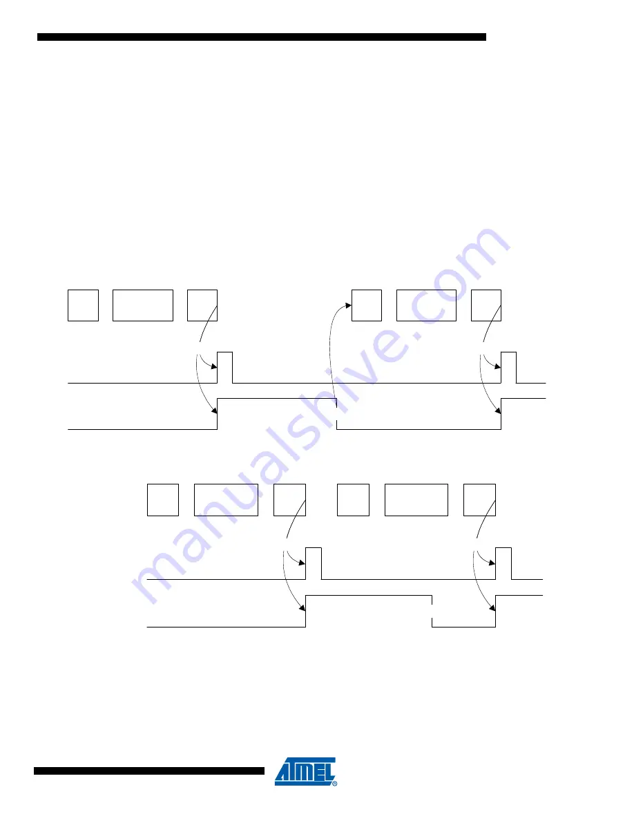
Figure 27-24. Example of an IN Pipe with 1 Data Bank
Figure 27-25. Example of an IN Pipe with 2 Data Banks
27.7.3.11
Management of OUT pipes
OUT packets are sent by the host. All the data can be written which acknowledges or not the
bank when it is full.
The pipe must be configured and unfrozen first.
IN
DATA
(bank 0)
ACK
RXINI
FIFOCON
HW
IN
DATA
(bank 0)
ACK
HW
SW
SW
SW
read data from CPU
BANK 0
read data from CPU
BANK 0
IN
DATA
(bank 0)
ACK
RXINI
FIFOCON
HW
IN
DATA
(bank 1)
ACK
SW
SW
read data from CPU
BANK 0
HW
SW
read data from CPU
BANK 1
Summary of Contents for AT32UC3A3128
Page 61: ...61 32072H AVR32 10 2012 AT32UC3A3 PLLEN PLL Enable 0 PLL is disabled 1 PLL is enabled...
Page 592: ...592 32072H AVR32 10 2012 AT32UC3A3 Manchester Configuration Register on page 614...
Page 989: ...989 32072H AVR32 10 2012 AT32UC3A3 37 2 Package Drawings Figure 37 1 TFBGA 144 package drawing...
Page 991: ...991 32072H AVR32 10 2012 AT32UC3A3 Figure 37 3 VFBGA 100 package drawing...


