CHIP-SELECT UNIT
6-16
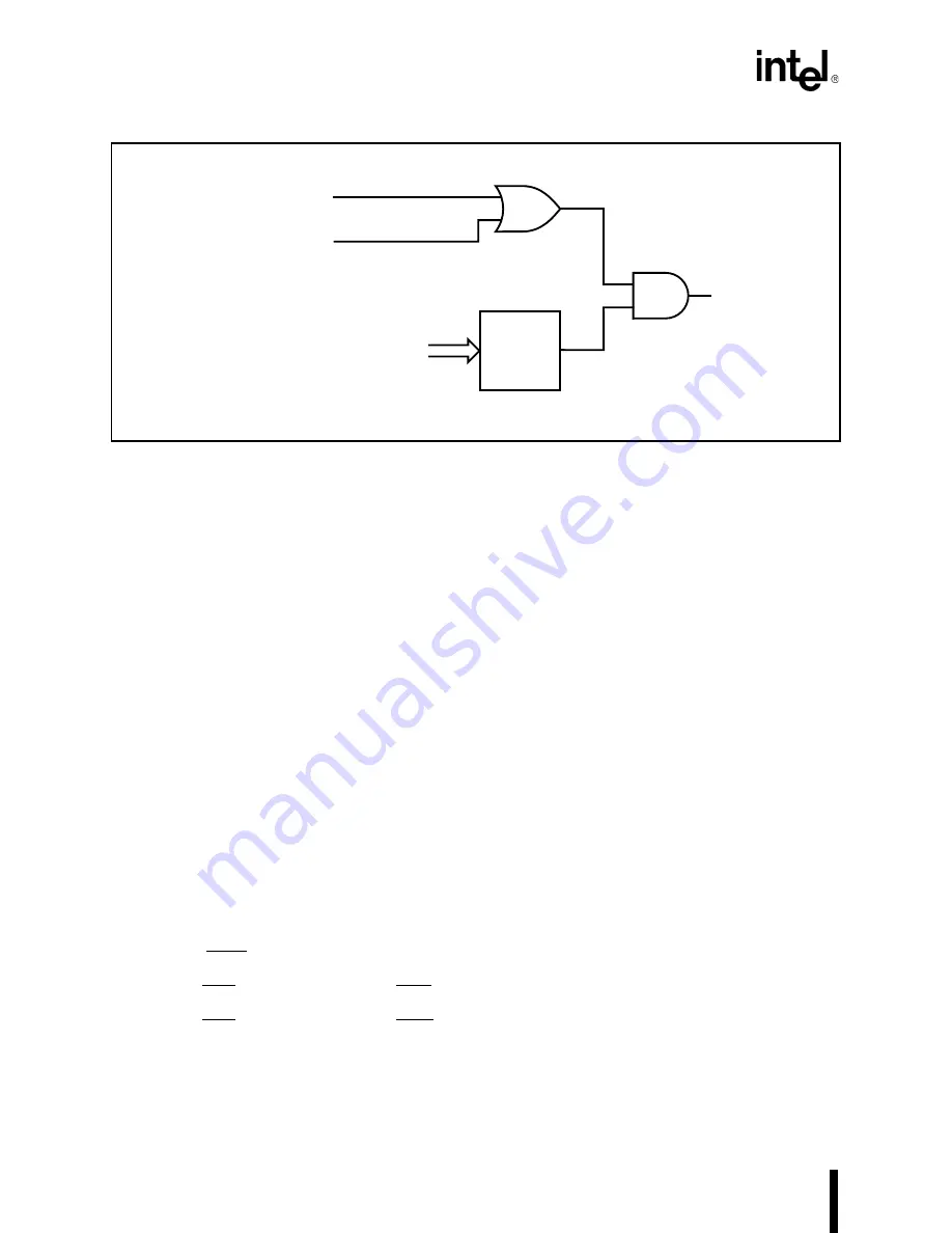
Figure 6-11. Wait State and Ready Control Functions
The R2 control bit determines whether the bus cycle completes normally (requires bus ready) or
unconditionally (ignores bus ready). The R1:0 bits define the number of wait states to insert into
the bus cycle. For devices requiring three or fewer wait states, you can set R2 (ignore bus ready)
and program R1:0 with the number of required wait states. For devices that may require more than
three wait states, you must clear R2 (require bus ready).
A bus cycle with wait states automatically inserted cannot be shortened. A bus cycle that ignores
bus ready cannot be lengthened.
6.4.4
Overlapping Chip-Selects
The Chip-Select Unit activates all enabled chip-selects programmed to cover the same physical
address space. This is true if any portion of the chip-selects’ address ranges overlap (i.e., chip-
selects’ ranges do not need to overlap completely to all go active). There are various reasons for
overlapping chip-selects. For example, a system might have a need for overlapping a portion of
read-only memory with read/write memory or copying data to two devices simultaneously.
If overlapping chip-selects do not have identical wait state and bus ready programming, the Chip-
Select Unit uses the following priority scheme:
1.
If any MCS chip-select is active, it uses the R2:0 bits in the MPCS register.
2.
If the PCS chip-selects overlap LCS, it uses the R2:0 bits in the LMCS register.
3.
If the PCS chip-selects overlap UCS, it uses the R2:0 bits in the UMCS register.
Wait State Value (R1:0)
READY
R2 Control Bit
Wait
State
Counter
BUS READY
Wait
State
Ready
A1137-0A
Summary of Contents for 80C186XL
Page 1: ...80C186XL 80C188XL Microprocessor User s Manual...
Page 2: ...80C186XL 80C188XL Microprocessor User s Manual 1995...
Page 18: ...1 Introduction...
Page 19: ......
Page 27: ......
Page 28: ...2 Overview of the 80C186 Family Architecture...
Page 29: ......
Page 79: ......
Page 80: ...3 Bus Interface Unit...
Page 81: ......
Page 127: ......
Page 128: ...4 Peripheral Control Block...
Page 129: ......
Page 137: ......
Page 138: ...5 ClockGenerationand Power Management...
Page 139: ......
Page 154: ...6 Chip Select Unit...
Page 155: ......
Page 178: ...7 Refresh Control Unit...
Page 179: ......
Page 193: ......
Page 194: ...8 Interrupt Control Unit...
Page 195: ......
Page 227: ......
Page 228: ...9 Timer Counter Unit...
Page 229: ......
Page 253: ......
Page 254: ...10 Direct Memory Access Unit...
Page 255: ......
Page 283: ......
Page 284: ...11 Math Coprocessing...
Page 285: ......
Page 302: ...12 ONCE Mode...
Page 303: ......
Page 306: ...A 80C186 Instruction Set Additions and Extensions...
Page 307: ......
Page 318: ...B Input Synchronization...
Page 319: ......
Page 322: ...C Instruction Set Descriptions...
Page 323: ......
Page 371: ......
Page 372: ...D Instruction Set Opcodes and Clock Cycles...
Page 373: ......
Page 396: ...Index...
Page 397: ......


