10-5
DIRECT MEMORY ACCESS UNIT
10.1.4.1
Source Synchronization
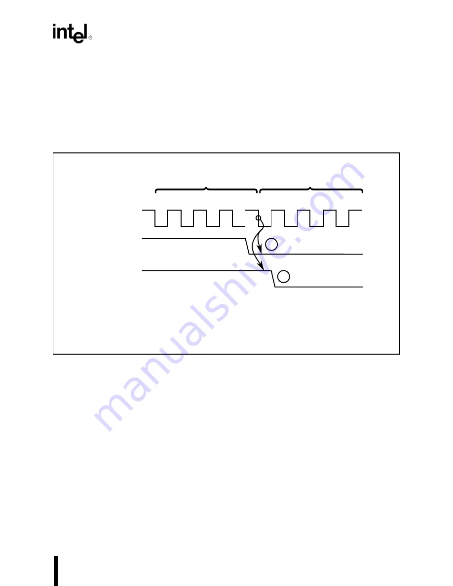
A typical source-synchronized transfer is shown in Figure 10-3. Most DMA-driven peripherals
deassert their DRQ line only after the DMA transfer has begun. The DRQ signal must be deas-
serted at least four clocks before the end of the DMA transfer (at the T1 state of the deposit phase)
to prevent another DMA cycle from occurring. A source-synchronized transfer provides the
source device at least three clock cycles from the time it is accessed (acknowledged) to deassert
its request line if further transfers are not required.
Figure 10-3. Source-Synchronized Transfers
10.1.4.2
Destination Synchronization
A destination-synchronized transfer differs from a source-synchronized transfer by the addition
of two idle states at the end of the deposit cycle (Figure 10-4). The two idle states extend the DMA
cycle to allow the destination device to deassert its DRQ pin four clocks before the end of the
cycle. If the two idle states were not inserted, the destination device would not be able to deassert
its request in time to prevent another DMA cycle from occurring.
The insertion of two idle states at the end of a destination synchronization transfer has an impor-
tant side effect. A destination-synchronized DMA channel gives up the bus during the idle
states, allowing any other bus master to gain ownership. This includes the CPU, the Refresh
Control Unit, an external bus master or another DMA channel.
T1
T2
T3
T4
CLKOUT
DRQ (Case 1)
T1
T2
T3
T4
DRQ (Case 2)
Fetch Cycle
Deposit Cycle
NOTES:
1. Current source synchronized transfer will not be immediately
followed by another DMA transfer.
2. Current source synchronized transfer will be immediately
followed by another DMA transfer.
2
1
A1188-0A
Summary of Contents for 80C186XL
Page 1: ...80C186XL 80C188XL Microprocessor User s Manual...
Page 2: ...80C186XL 80C188XL Microprocessor User s Manual 1995...
Page 18: ...1 Introduction...
Page 19: ......
Page 27: ......
Page 28: ...2 Overview of the 80C186 Family Architecture...
Page 29: ......
Page 79: ......
Page 80: ...3 Bus Interface Unit...
Page 81: ......
Page 127: ......
Page 128: ...4 Peripheral Control Block...
Page 129: ......
Page 137: ......
Page 138: ...5 ClockGenerationand Power Management...
Page 139: ......
Page 154: ...6 Chip Select Unit...
Page 155: ......
Page 178: ...7 Refresh Control Unit...
Page 179: ......
Page 193: ......
Page 194: ...8 Interrupt Control Unit...
Page 195: ......
Page 227: ......
Page 228: ...9 Timer Counter Unit...
Page 229: ......
Page 253: ......
Page 254: ...10 Direct Memory Access Unit...
Page 255: ......
Page 283: ......
Page 284: ...11 Math Coprocessing...
Page 285: ......
Page 302: ...12 ONCE Mode...
Page 303: ......
Page 306: ...A 80C186 Instruction Set Additions and Extensions...
Page 307: ......
Page 318: ...B Input Synchronization...
Page 319: ......
Page 322: ...C Instruction Set Descriptions...
Page 323: ......
Page 371: ......
Page 372: ...D Instruction Set Opcodes and Clock Cycles...
Page 373: ......
Page 396: ...Index...
Page 397: ......


