Chapter 3 Signals
3-11
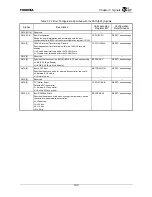
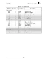
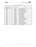
Table 3.2.2 Boot Configuration Specified with the ADDR[19:0] Signals (1/2)
Signal Description
Corresponding
Register Bit
Configuration
Determined at
ADDR[19] PCI
Controller Mode Select
Specifies the operating mode of the TX4937 PCI controller.
L = Satellite
H = Host
CCFG. PCIMODE
RESET
*
deassert edge
ADDR[18]
Select Shared I/O Pins
Specifies the function of the PIO[15:8]/CB[7:0] shared pins.
L = PIO[15:8]
H = CB[7:0]
PCFG. SEL1
RESET
*
deassert edge
ADDR[17:15] Reserved
Used for testing. This signal will not be set to 0 upon booting.
⎯
⎯
ADDR[14:13] Select SYSCLK Frequency
Specifies the division ratio of the SYSCLK frequency to the G-Bus
clock (GBUSCLK) frequency.
LL = 4 (SYSCLK frequency = GBUSCLK frequency/4)
LH = 3 (SYSCLK frequency = GBUSCLK frequency/3)
HL = 2 (SYSCLK frequency = GBUSCLK frequency/2)
HH = 1 (SYSCLK frequency = GBUSCLK frequency)
CCFG. SYSSP
CGRESET
*
deassert
edge
ADDR[12] TX4937
Endian
Mode
Specifies the TX4937 endian mode.
L = Little endian
H = Big endian
CCFG. ENDIAN
RESET
*
deassert edge
ADDR[11:10] Select PCI Clock Frequency
Specifies the division ratio of the PCI bus clock (PCICLK[5:0]) to the
TX49/H3 core clock (CPUCLK). Initial value of CCFG[12] is 0.
LL = 8 (PCICLK frequency = CPUCLK frequency/8)
LH = 9 (PCICLK frequency = CPUCLK frequency/9)
HL = 10 (PCICLK frequency = CPUCLK frequency/10)
HH = 11 (PCICLK frequency = CPUCLK frequency/11)
CCFG. PCIDIVMODE CGRESET
*
deassert
edge
ADDR[9] PIO[4:2]/ACLC/DMAREQ[2]/DMAACK[2]
Select
Specifies whether PIO[4:2]/DMAREQ[2]/DMAACK[2] signals are
used as PIO or AC-link interface signals.
L = PIO
H = AC-link interface
PCFG.SEL2 RESET
*
deassert edge
ADDR[8:6]
Select Boot Memory and Device Clock Frequency
Specifies the clock division ratio for external bus controller channel 0
upon booting (refer to Section “7.3.8 Clock Options”).
HHH = Device connected to channel 0 of the external bus controller
(Clock division rate = 1/1)
HHL = Device connected to channel 0 of the external bus controller
(Clock division rate = 1/2)
HLH = Device connected to channel 0 of the external bus controller
(Clock division rate = 1/3)
HLL = Device connected to channel 0 of the external bus controller
(Clock division rate = 1/4)
LHH =PCI boot
LHL = Reserved
LLH and LLL = Reserved
ADDR[8]:
EBCCR0.ME
ADDR[7:6]
EBCCR0.SP
RESET
*
deassert edge
ADDR[5]
Select SDRAM device
Select initial setting derivability of SDRAM interface signals
L = 8mA
H = 16mA
ADDR[19:0], CKE, RAS
*
, CAS
*
, WE
*
, SDCS[3:0], SDCLK[3:0],
SDCLKIN
PCFG[53:40]
RESET
*
deassert edge
Summary of Contents for TX49 TMPR4937
Page 1: ...64 Bit TX System RISC TX49 Family TMPR4937 Rev 2 0 ...
Page 4: ......
Page 13: ...Table of Contents ix TMPR4937 Revision History 1 ...
Page 14: ...Table of Contents x ...
Page 15: ...Handling Precautions ...
Page 16: ......
Page 18: ...1 Using Toshiba Semiconductors Safely 1 2 ...
Page 40: ...3 General Safety Precautions and Usage Considerations 3 18 ...
Page 42: ...4 Precautions and Usage Considerations 4 2 ...
Page 43: ...TMPR4937 2005 3 Rev 2 0 ...
Page 44: ......
Page 52: ...Chapter 1 Overview and Features 1 6 ...
Page 156: ...Chapter 7 External Bus Controller 7 56 ...
Page 491: ...Chapter 16 Removed 16 1 16 Removed ...
Page 492: ...Chapter 16 Removed 16 2 ...
Page 493: ...Chapter 17 Removed 17 1 17 Removed ...
Page 494: ...Chapter 17 Removed 17 2 ...
Page 495: ...Chapter 18 Removed 18 1 18 Removed ...
Page 496: ...Chapter 18 Removed 18 2 ...
Page 497: ...Chapter 19 Removed 19 1 19 Removed ...
Page 498: ...Chapter 19 Removed 19 2 ...
Page 506: ...Chapter 20 Extended EJTAG Interface 20 8 ...
Page 530: ...Chapter 22 Pinout and Package Information 22 10 ...
Page 542: ...Chapter 24 Parts Number when Ordering 24 2 ...


