Chapter 5 Configuration Registers
5-4
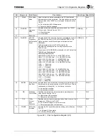
Bit
Mnemonic Field Name
Description
Initial Value Read/Write
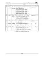
23 PCI66
PCI 66MHz
Mode
Used to inform the device connected to the PCI bus that a 66
MHz operation is to be performed. This bit is valid only when the
PCI controller of the TX4937 is in host mode. (Refer to Section
10.3.8.)
0 = Do not perform a 66 MHz operation.
1 = Perform a 66 MHz operation.
0 R/W
22 PCIMODE
PCI
Operation
Mode
Indicates information about the operation mode of the TX4937
PCI controller. (Refer to Section 10.3.1.)
L: 0: Satellite mode
H: 1: Host mode
ADDR[19] R
21
⎯
Reserved
⎯
⎯
⎯
20:17 DIVMODE CPUCLK
Frequency
Multiplication
Factor
Indicates information about the frequency multiplication factor of
the TX49/H3 core clock (CPUCLK) to the MASTERCLK. This
field is set with a result of encoding an initial input value at
ADDR[3:0].
The PLL incorporated in the TX4937 multiplies the
MASTERCLK and supplies the resulting frequency to the
TX49/H3 core.
The value set in DIVMODE[3:0] is reflected in the EC field of the
TX49/H3 core Config register.
ADDR[3:0]:DIVMODE[3:0]
HHHH: 0100: CPUCLK freq.
=
2
×
MASTERCLK freq.
HHHL: 1111: CPUCLK freq.
=
2.5
×
MASTERCLK freq.
HHLH: 0101: CPUCLK freq.
=
3
×
MASTERCLK freq.
HHLL: 0110: CPUCLK freq.
=
4
×
MASTERCLK freq.
LHHH: 1101: CPUCLK freq. = 4.5 x MASTERCLK freq.
LHHL: ---- : Reserved
LHLH: ---- : Reserved
LHLL: ---- : Reserved
HLHH: 0000: CPUCLK freq.
=
8
×
MASTERCLK freq.
HLHL: 1011: CPUCLK freq.
=
10
×
MASTERCLK freq.
HLLH: 0001: CPUCLK freq.
=
12
×
MASTERCLK freq.
HLLL: 0010: CPUCLK freq.
=
16
×
MASTERCLK freq.
LLHH: 1001: CPUCLK freq.
=
18
×
MASTERCLK freq.
LLHL: ---- : Reserved
LLLH: ---- : Reserved
LLLL: ---- : Reserved
ADDR[3:0] R
16 BEOW
Write-Access
Bus Error
Indicates that a timeout error has occurred in the internal bus (G-
Bus) during a write bus transaction of the TX49/H3 core. This bit
corresponds to interrupt No. 1 in the interrupt controller.
0 = No error has occurred.
1 = An error has occurred.
0 R/W1C
15 WR
Watchdog
Timer Mode
Specifies how information will be reported in watchdog timer
mode (refer to Section 12.3.6).
0 = Generate an NMI exception.
1 = Generate a watchdog reset.
0 R/W
14 TOE
G-Bus
Timeout
Error
Detection
Specifies whether to detect and report a bus timeout error in the
internal bus (G-Bus) of the TX4937.
0 = Do not detect or report a bus timeout error.
1 = Detect and report a bus timeout error.
0 R/W
13 PCIARB
PCI Arbiter
Selection
Indicates the PCI bus arbiter selection setting (refer to Section
10.3.12).
L: 0 = External PCI bus arbiter
H: 1 = Built-in PCI bus arbiter
DATA[2] R
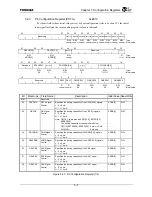
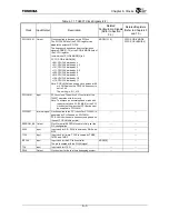
Figure 5.2.1 Chip Configuration Register (2/3)
Summary of Contents for TX49 TMPR4937
Page 1: ...64 Bit TX System RISC TX49 Family TMPR4937 Rev 2 0 ...
Page 4: ......
Page 13: ...Table of Contents ix TMPR4937 Revision History 1 ...
Page 14: ...Table of Contents x ...
Page 15: ...Handling Precautions ...
Page 16: ......
Page 18: ...1 Using Toshiba Semiconductors Safely 1 2 ...
Page 40: ...3 General Safety Precautions and Usage Considerations 3 18 ...
Page 42: ...4 Precautions and Usage Considerations 4 2 ...
Page 43: ...TMPR4937 2005 3 Rev 2 0 ...
Page 44: ......
Page 52: ...Chapter 1 Overview and Features 1 6 ...
Page 156: ...Chapter 7 External Bus Controller 7 56 ...
Page 491: ...Chapter 16 Removed 16 1 16 Removed ...
Page 492: ...Chapter 16 Removed 16 2 ...
Page 493: ...Chapter 17 Removed 17 1 17 Removed ...
Page 494: ...Chapter 17 Removed 17 2 ...
Page 495: ...Chapter 18 Removed 18 1 18 Removed ...
Page 496: ...Chapter 18 Removed 18 2 ...
Page 497: ...Chapter 19 Removed 19 1 19 Removed ...
Page 498: ...Chapter 19 Removed 19 2 ...
Page 506: ...Chapter 20 Extended EJTAG Interface 20 8 ...
Page 530: ...Chapter 22 Pinout and Package Information 22 10 ...
Page 542: ...Chapter 24 Parts Number when Ordering 24 2 ...

