Chapter 9 SDRAM Controller
9-7
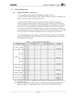
9.3.2.3 Address Signal Mapping (32-bit Data Bus)
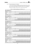
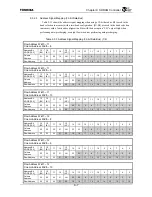
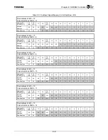
Table 9.3.3 shows the address signal mapping when using a 32-bit data bus. B0 is used in the
bank selection in memory with a two-bank configuration. [B1:B0] are used in the bank selection
in memory with a four-bank configuration. Bits with the description "L/H" output High when
performing auto-precharging, or output Low when not performing auto-precharging.
Table 9.3.3 Address Signal Mapping (32-bit Data Bus) (1/2)
Row Address Width
=
11
Column Address Width
=
8
Address Bit
ADDR [19:5]
19
(B0)
18
(B1)
17 16
15
(AP)
14 13 12 11 10 9 8 7 6 5
Column
Address
21 22 20 19 L/H L/H L/H 9
8
7
6
5
4
3
2
Row
Address 21 22 20 19 20
19
18
17
16
15
14
13
12
11
10
Row Address Width
=
11
Column Address Width
=
9
Address Bit
ADDR [19:5]
19
(B0)
18
(B1)
17 16
15
(AP)
14 13 12 11 10 9 8 7 6 5
Column
Address
22 22 22 22 L/H 22 21
9
8
7
6
5
4
3
2
Row
Address 22 22 22 22 20
19
18
17
16
15
14
13
12
11
10
Row Address Width
=
11
Column Address Width
=
10
Address Bit
ADDR [19:5]
19
(B0)
18
(B1)
17 16
15
(AP)
14 13 12 11 10 9 8 7 6 5
Column
Address
23 22 22 23 L/H 22
21
9
8
7
6
5
4
3
2
Row
Address 23 22 22 23 20
19
18
17
16
15
14
13
12
11
10
Row Address Width
=
12
Column Address Width
=
8
Address Bit
ADDR [19:5]
19
(B0)
18
(B1)
17 16
15
(AP)
14 13 12 11 10 9 8 7 6 5
Column
Address
22 23 22 21 L/H 23 22 9
8
7
6
5
4
3
2
Row Address
22
23
22
21
20
19
18
17
16
15
14
13
12
11
10
Row Address Width
=
12
Column Address Width
=
9
Address Bit
ADDR [19:5]
19
(B0)
18
(B1)
17 16
15
(AP)
14 13 12 11 10 9 8 7 6 5
Column
Address
23 24 23 21 L/H 23 22
9
8
7
6
5
4
3
2
Row Address
23
24
23
21
20
19
18
17
16
15
14
13
12
11
10
Row Address Width
=
12
Column Address Width
=
10
Address Bit
ADDR [19:5]
19
(B0)
18
(B1)
17 16
15
(AP)
14 13 12 11 10 9 8 7 6 5
Column
Address
24 25 24 21 L/H 23
22
9
8
7
6
5
4
3
2
Row Address
24
25
24
21
20
19
18
17
16
15
14
13
12
11
10
Summary of Contents for TX49 TMPR4937
Page 1: ...64 Bit TX System RISC TX49 Family TMPR4937 Rev 2 0 ...
Page 4: ......
Page 13: ...Table of Contents ix TMPR4937 Revision History 1 ...
Page 14: ...Table of Contents x ...
Page 15: ...Handling Precautions ...
Page 16: ......
Page 18: ...1 Using Toshiba Semiconductors Safely 1 2 ...
Page 40: ...3 General Safety Precautions and Usage Considerations 3 18 ...
Page 42: ...4 Precautions and Usage Considerations 4 2 ...
Page 43: ...TMPR4937 2005 3 Rev 2 0 ...
Page 44: ......
Page 52: ...Chapter 1 Overview and Features 1 6 ...
Page 156: ...Chapter 7 External Bus Controller 7 56 ...
Page 491: ...Chapter 16 Removed 16 1 16 Removed ...
Page 492: ...Chapter 16 Removed 16 2 ...
Page 493: ...Chapter 17 Removed 17 1 17 Removed ...
Page 494: ...Chapter 17 Removed 17 2 ...
Page 495: ...Chapter 18 Removed 18 1 18 Removed ...
Page 496: ...Chapter 18 Removed 18 2 ...
Page 497: ...Chapter 19 Removed 19 1 19 Removed ...
Page 498: ...Chapter 19 Removed 19 2 ...
Page 506: ...Chapter 20 Extended EJTAG Interface 20 8 ...
Page 530: ...Chapter 22 Pinout and Package Information 22 10 ...
Page 542: ...Chapter 24 Parts Number when Ordering 24 2 ...

