Chapter 5 Configuration Registers
5-7
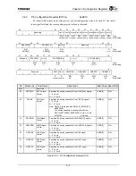
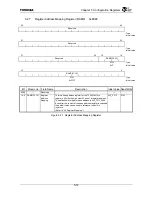
5.2.3 Pin
Configuration
Register (PCFG)
0xE010
For the bit fields whose initial values are set by boot configuration (refer to Section 3.2), the initial
input signal level and the corresponding register value are indicated.
63
57 56 55 54 53 52 51 50 49 48
Reserved
DRVDATA
DRVCB DRVDQM
DRVADDR
DRVCKE DRVRAS DRVCAS DRVWE
DRVCS[3]
R/W
R/W
R/W
R/W
R/W
R/W
R/W
R/W
R/W
:
Type
ADDR[4] ADDR[4] ADDR[4] ADDR[5] ADDR[5] ADDR[5] ADDR[5] ADDR[5] ADDR[5]
: Initial value
47 45 44 41 40 39 33 32
DRVCS[2:0]
DRVCK[3:0]
DRVCKIN
Reserved
BYPASSPLL
R/W
R/W
R/W
R
:
Type
ADDR[5]
ADDR[5]
ADDR[5]
BYPASSPLL
*
: Initial value
31 30 29 28 27 26 23 22 21
16
Reserved SDCLKDLY
SYSCLKEN
SDCLKEN[3:0]
SDCLKINEN
PCICLKEN[5:0]
R/W
R/W
R/W
R/W
R/W
:
Type
00 1
1111
0
111111
:
Initial
value
15 10
9 8 7 0
Reserved SEL2 SEL1
DMASEL3
DMASEL2
DMASEL1
DMASEL0
R
R R/W
R/W
R/W
R/W
:
Type
ADDR[9] ADDR[18]
00 00 00 00
:
Initial
value
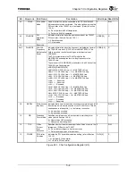
Bit
Mnemonic Field Name
Description
Initial Value Read/Write
63:57
⎯
Reserved
⎯
⎯
⎯
56 DRVDATA
DATA Signal
Control
Specifies the driving capability of the DATA[63:0] signals.
L : 0 = 8 mA
H : 1 = 16 mA
ADDR[4] R/W
55 DRVCB
CB Signal
Control
Specifies the driving capability of the CB[7:0]
*
signals.
L : 0 = 8 mA
H : 1 = 16 mA
Note: CB[7:0}
*
share pins with PIO[15:8], E0TXD[3:0],
E0RXD[3:0].
The driving capability of these pins are below.
CB[7:0], E0TXD[3:0], E0RXD[3:0]: 8 mA or 16 mA
PIO[15:8]:
8
mA
only
ADDR[4] R/W
54 DRVDQM
DQM Signal
Control
Specifies the driving capability of the DQM[7:0]
*
signals.
L : 0 = 8 mA
H : 1 = 16 mA
ADDR[4] R/W
53 DRVADDR
ADDR Signal
Control
Specifies the driving capability of the ADDR[19:0] signals.
L : 0 = 8 mA
H : 1 = 16 mA
ADDR[5] R/W
52 DRVCKE
CKE Signal
Control
Specifies the driving capability of the CKE signal.
L : 0 = 8 mA
H : 1 = 16 mA
ADDR[5] R/W
51 DRVRAS
RAS Signal
Control
Specifies the driving capability of the RAS
*
signal.
L : 0 = 8 mA
H : 1 = 16 mA
ADDR[5] R/W
50 DRVCAS
CAS Signal
Control
Specifies the driving capability of the CAS
*
signal.
L : 0 = 8 mA
H : 1 = 16 mA
ADDR[5] R/W
Figure 5.2.3 Pin Configuration Register (1/3)
Summary of Contents for TX49 TMPR4937
Page 1: ...64 Bit TX System RISC TX49 Family TMPR4937 Rev 2 0 ...
Page 4: ......
Page 13: ...Table of Contents ix TMPR4937 Revision History 1 ...
Page 14: ...Table of Contents x ...
Page 15: ...Handling Precautions ...
Page 16: ......
Page 18: ...1 Using Toshiba Semiconductors Safely 1 2 ...
Page 40: ...3 General Safety Precautions and Usage Considerations 3 18 ...
Page 42: ...4 Precautions and Usage Considerations 4 2 ...
Page 43: ...TMPR4937 2005 3 Rev 2 0 ...
Page 44: ......
Page 52: ...Chapter 1 Overview and Features 1 6 ...
Page 156: ...Chapter 7 External Bus Controller 7 56 ...
Page 491: ...Chapter 16 Removed 16 1 16 Removed ...
Page 492: ...Chapter 16 Removed 16 2 ...
Page 493: ...Chapter 17 Removed 17 1 17 Removed ...
Page 494: ...Chapter 17 Removed 17 2 ...
Page 495: ...Chapter 18 Removed 18 1 18 Removed ...
Page 496: ...Chapter 18 Removed 18 2 ...
Page 497: ...Chapter 19 Removed 19 1 19 Removed ...
Page 498: ...Chapter 19 Removed 19 2 ...
Page 506: ...Chapter 20 Extended EJTAG Interface 20 8 ...
Page 530: ...Chapter 22 Pinout and Package Information 22 10 ...
Page 542: ...Chapter 24 Parts Number when Ordering 24 2 ...

