Chapter 9 SDRAM Controller
9-12
9.3.6 Bus
Errors
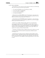
The SDRAMC detects bus errors in the following situations:
•
Bus time-out occurs during Read or Write operation to the SDRAMC
•
ECC 2-bit fault error or Parity error occurs during SDRAM Read operation
If a bus error occurs when accessing the SDRAMC, then the SDRAMC will immediately assert the
current operation. Then, the current SDRAM cycle will end, remaining SDRAMC operations will be
aborted, a Pre-charge All command will be issued to SDRAM, then the SDRAMC will return to the Idle
state.
9.3.7
Memory Read and Memory Write
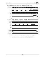
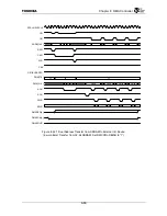
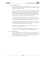
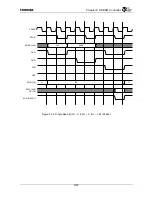
The RAS* signal, CAS* signal, WE*, signal, and ADDR[19:5] signal are set up 1 cycle before the
SDCS* signal is asserted in the case of the Read command, Write command, Pre-charge command, or
Mode Register Set command. The same set up time is observed even for active commands if the Active
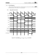
Command Ready bit (SDCTR.DA) of the SDRAM Timing Register is set. Figure 9.5.1 is a timing
diagram of Single Read operation when the SDCTR.DA bit is cleared. Figure 9.5.2 is a timing diagram
of Single Read operation when the SDCTR.DA bit is set.
Burst or Single Read operation is terminated by the Pre-charge Active Bank command. Burst or
Single Write operation is terminated by the Auto Pre-charge Command.
9.3.8 Slow
Write
Burst
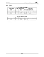
When the Slow Write Burst bit (SDCTR.SWB) of the SDRAM Timing Register is cleared, the data
changes at each cycle during Burst Write operation (Figure 9.5.6). When the Slow Write Burst bit is set,
the data will change every other cycle (Figure 9.5.7).
When the Slow Write Burst bit is set, all Write accesses will operate as t
RCD
= 3t
CK
regardless of the
setting of the RAS-CAS Delay bit (SDCTR.RCD) of the SDRAM Timing Register. The RAS-CAS
Delay bit setting becomes valid when Slow Write Burst access is invalid. The setting of the Slow Burst
bit does not have any effect on Read access.
9.3.9 Clock
Feedback
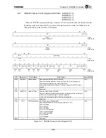
When performing Read access at fast rates like 100 MHz, there may be insufficient set up time if an
attempt to directly latch Read data with the internal clock is made. With the TX4937, it is possible to
latch data using SDRAM clock SDCLKIN that is input from outside the chip. Please connect
SDCLKIN to one of the SDCLK[3:0] pins and the external source.
Summary of Contents for TX49 TMPR4937
Page 1: ...64 Bit TX System RISC TX49 Family TMPR4937 Rev 2 0 ...
Page 4: ......
Page 13: ...Table of Contents ix TMPR4937 Revision History 1 ...
Page 14: ...Table of Contents x ...
Page 15: ...Handling Precautions ...
Page 16: ......
Page 18: ...1 Using Toshiba Semiconductors Safely 1 2 ...
Page 40: ...3 General Safety Precautions and Usage Considerations 3 18 ...
Page 42: ...4 Precautions and Usage Considerations 4 2 ...
Page 43: ...TMPR4937 2005 3 Rev 2 0 ...
Page 44: ......
Page 52: ...Chapter 1 Overview and Features 1 6 ...
Page 156: ...Chapter 7 External Bus Controller 7 56 ...
Page 491: ...Chapter 16 Removed 16 1 16 Removed ...
Page 492: ...Chapter 16 Removed 16 2 ...
Page 493: ...Chapter 17 Removed 17 1 17 Removed ...
Page 494: ...Chapter 17 Removed 17 2 ...
Page 495: ...Chapter 18 Removed 18 1 18 Removed ...
Page 496: ...Chapter 18 Removed 18 2 ...
Page 497: ...Chapter 19 Removed 19 1 19 Removed ...
Page 498: ...Chapter 19 Removed 19 2 ...
Page 506: ...Chapter 20 Extended EJTAG Interface 20 8 ...
Page 530: ...Chapter 22 Pinout and Package Information 22 10 ...
Page 542: ...Chapter 24 Parts Number when Ordering 24 2 ...


