Chapter 5 Configuration Registers
5-3
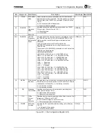
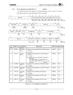
5.2.1 Chip
Configuration
Register (CCFG)
0xE000
For the bit fields whose initial values are set by boot configuration (refer to Section 3.2), the initial
input signal level and the corresponding register value are indicated.
63
48
Reserved
: Type
: Initial value
47 42
41
40
39 32
Reserved
WDRST
WDREXEN
BCFG
R/W1C R/W
R
:
Type
0 0
DATA[15:8]
:
Initial
value
31 27 26 25 24 23 22 21 20 17 16
Reserved
GTOT
TINTDIS
PCI66
PCIMODE
PCI1-66
DIVMODE BEOW
R/W R
R/W
R
R/W
R
R/W1C
:
Type
11
~DATA[7]
0
ADDR[19]
0
ADDR[3:0]
0
: Initial value
15 14 13
12 10 9 8 7 6 5 3 2 1 0
WR TOE
PCIARB
PCIDIVMODE Reserved SYSSP
Reserved
ENDIAN
ARMODE
ACEHOLD
R/W
R/W
R
R/W
R/W
R
R
R/W
R/W
:
Type
0 0
DATA[2]
ADDR[11:10]
0
ADDR[14:13]
ADDR[12]
0
1
: Initial value
Bit
Mnemonic Field Name
Description
Initial Value Read/Write
63:42
⎯
Reserved
⎯
⎯
⎯
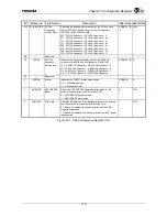
41 WDRST
Watchdog
Reset Status
Watch Dog Reset Status (Initial Value 0, RW1C)
Indicates that a watchdog reset has occurred (refer to Section
12.3.6).
Initialized when CGRESET
*
is asserted.
0
=
No watchdog reset has occurred.
1
=
A watchdog reset has occurred
0 R/W1C
40 WDREXEN
Watchdog
Reset External
Output
Watch Dog Reset External Enable (Initial Value 0, R/W)
Specifies whether to assert the WDRST
*
signal at a watchdog
reset (refer to Section 12.3.6).
Initialized when CGRESET
*
is asserted.
0
=
Do not assert the WDRST
*
signal.
1
=
Assert the WDRST
*
signal.
0 R/W
39:32 BCFG Boot
Configuration
Set to 1 at a reset if the corresponding DATA[15:8] signal is
high.
Set to 0 at a reset if the corresponding DATA[15:8] signal is
low.
DATA[15:8]
R
31:27
⎯
Reserved
⎯
⎯
⎯
26:25 GTOT G-Bus Timeout
Time
Specifies the number of G-Bus clock (GBUSCLK) cycles after
which a bus timeout error will occur on the internal bus (G-
Bus) of the TX4937.
11
=
4096 GBUSCLK
10
=
2048 GBUSCLK
01
=
1024 GBUSCLK
00
=
512 GBUSCLK
11
R/W
24 TINTDIS
Disable
TX49/H3 Core
Timer Interrupt
Indicates a value for indicating whether to enable the
TX49/H3 internal timer interrupt (refer to Section 15.3.5).
H: 0: The TX49/H3 internal timer interrupt is enabled.
L: 1: The TX49/H3 internal timer interrupt is disabled.
~DATA[7]
R
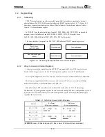
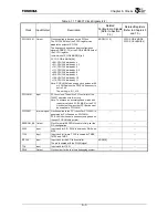
Figure 5.2.1 Chip Configuration Register (1/3)
Summary of Contents for TX49 TMPR4937
Page 1: ...64 Bit TX System RISC TX49 Family TMPR4937 Rev 2 0 ...
Page 4: ......
Page 13: ...Table of Contents ix TMPR4937 Revision History 1 ...
Page 14: ...Table of Contents x ...
Page 15: ...Handling Precautions ...
Page 16: ......
Page 18: ...1 Using Toshiba Semiconductors Safely 1 2 ...
Page 40: ...3 General Safety Precautions and Usage Considerations 3 18 ...
Page 42: ...4 Precautions and Usage Considerations 4 2 ...
Page 43: ...TMPR4937 2005 3 Rev 2 0 ...
Page 44: ......
Page 52: ...Chapter 1 Overview and Features 1 6 ...
Page 156: ...Chapter 7 External Bus Controller 7 56 ...
Page 491: ...Chapter 16 Removed 16 1 16 Removed ...
Page 492: ...Chapter 16 Removed 16 2 ...
Page 493: ...Chapter 17 Removed 17 1 17 Removed ...
Page 494: ...Chapter 17 Removed 17 2 ...
Page 495: ...Chapter 18 Removed 18 1 18 Removed ...
Page 496: ...Chapter 18 Removed 18 2 ...
Page 497: ...Chapter 19 Removed 19 1 19 Removed ...
Page 498: ...Chapter 19 Removed 19 2 ...
Page 506: ...Chapter 20 Extended EJTAG Interface 20 8 ...
Page 530: ...Chapter 22 Pinout and Package Information 22 10 ...
Page 542: ...Chapter 24 Parts Number when Ordering 24 2 ...


