Chapter 9 SDRAM Controller
9-3
9.3 Detailed
Explanation
9.3.1 Supported
SDRAM
configurations
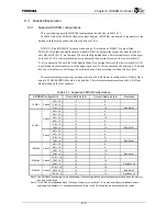
This controller supports the SDRAM configurations listed below in Table 9.3.1.
The MW field of the SDRAM Channel Control Register (SDCCRn) can be used to separately set the
data bus width for each channel to either 64 bits or 32 bits.
DATA[31:0] and DQM[3:0] are used when using a 32-bit data bus. DQM[7:4] output High.
DATA[63:32] output an undefined value when DATA[31:0] become the output, but enter the High-Z
state when DATA[31:0] are the input. When in the Big Endian Mode, first external access of the upper
word (bits 63:32) of the internal data bus is performed, then external access of the lower word (bits
31:0) is performed. When in the Little Endian Mode, first external access of the lower word (bits 31:0)
is performed, then external access of the upper word (bits 63:32) is performed. When using a 32-bit data
bus, two external access will always be performed even when accessing less than 32 bits of data.
The maximum memory capacity per channel when a 64-bit data bus is configured is 1 GBytes when
using 16 512-Mbit SDRAMs with a 4-bit data bus. The total maximum memory capacity is 4 GBytes
when totaling up the four channels.
Table 9.3.1 Supported SDRAM Configurations
SDRAM Configuration
Row Address (bit)
Column Address (bit)
Remarks
1 M
×
16
11
8
2 M
×
8
11
9
16 Mbit
2-bank
4 M
×
4
11
10
See Note 1
2 M
×
32
11
9
2 M
×
32
12
8
4 M
×
16
11
10
4 M
×
16
13
8
8 M
×
8
13
9
2-bank
16 M
×
4
13
10
See Note 1
2 M
×
32
11
8
4 M
×
16
12
8
8 M
×
8
12
9
64 Mbit
4-bank
16 M
×
4
12
10
See Note 1
4 M
×
32
12
8
8 M
×
16
12
9
16 M
×
8
12
10
128 Mbit
4-bank
32 M
×
4
12
11
See Note 1
16 M
×
16
13
9
32 M
×
8
13
10
256 Mbit
4-bank
64 M
×
4
13
11
See Note 1,2
32 M
×
16
13
10
64 M
×
8
13
11
See Note 2
512 Mbit
4-bank
128 M
×
4
13
12
See Note 1,2
Note1: The SDRAM Controller logic-wise does support these configurations, but please design carefully since the memory
bus load will be large.
Note2: This SDRAM configuration has 512 Mbytes of memory on a channel. If it is mapped to physical address space
beginning with address 0, it overlaps the address space for the ROM wherein the bootstrap vectors reside.
Summary of Contents for TX49 TMPR4937
Page 1: ...64 Bit TX System RISC TX49 Family TMPR4937 Rev 2 0 ...
Page 4: ......
Page 13: ...Table of Contents ix TMPR4937 Revision History 1 ...
Page 14: ...Table of Contents x ...
Page 15: ...Handling Precautions ...
Page 16: ......
Page 18: ...1 Using Toshiba Semiconductors Safely 1 2 ...
Page 40: ...3 General Safety Precautions and Usage Considerations 3 18 ...
Page 42: ...4 Precautions and Usage Considerations 4 2 ...
Page 43: ...TMPR4937 2005 3 Rev 2 0 ...
Page 44: ......
Page 52: ...Chapter 1 Overview and Features 1 6 ...
Page 156: ...Chapter 7 External Bus Controller 7 56 ...
Page 491: ...Chapter 16 Removed 16 1 16 Removed ...
Page 492: ...Chapter 16 Removed 16 2 ...
Page 493: ...Chapter 17 Removed 17 1 17 Removed ...
Page 494: ...Chapter 17 Removed 17 2 ...
Page 495: ...Chapter 18 Removed 18 1 18 Removed ...
Page 496: ...Chapter 18 Removed 18 2 ...
Page 497: ...Chapter 19 Removed 19 1 19 Removed ...
Page 498: ...Chapter 19 Removed 19 2 ...
Page 506: ...Chapter 20 Extended EJTAG Interface 20 8 ...
Page 530: ...Chapter 22 Pinout and Package Information 22 10 ...
Page 542: ...Chapter 24 Parts Number when Ordering 24 2 ...


