Chapter 11 Serial I/O Port
11-8
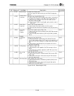
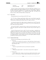
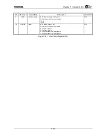
Transfer Size
1 Byte
DMCCRn.XFSZ = 000b
Transfer Address Mode
Dual
DMCCRn.SNGAD = 0
In the case of transmission channels, the address of the Transmit FIFO Register (SITFIFOn) is set in
the DMAC Destination Address Register (DMDARn). In the case of reception channels, the address of
the Receive FIFO Register (SIRFIFOn) is set in the DMAC Source Address Register (DMSARn).
Please set the addresses specified in “11.4.8 Transmit FIFO Register” and “11.4.9 Receive FIFO
Register” since the set address differs depending on the Endian mode.
11.3.7 Flow
Control
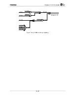
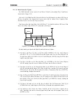
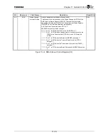
SIO supports hardware flow control that uses the RTS*/CTS* signal.
The CTS* (Clear to Send) input signal indicates that data can be received from the reception side
when it is Low. Setting the Transmission Enable Select bit (TES) of the Flow Control Register
(SIFLCRn) makes transmission flow control that uses the CTS* signal more effective.
It is also possible to generate status change interrupts by changing the state of the CTS* signal. The
conditions in which interrupts are generated can be selected by the CTSS Active Condition field of the
DMA/Interrupt Control Register (SIDICRn).
Setting the RTS* (Request to Send) output signal to High requests the transmission side to pause
transmission. Transmission resumes when the reception side becomes ready and the RTS* signal is set
to Low.
Setting the Reception Enable Select bit (RCS) of the flow Control Register (SIFLCRn) makes
reception flow control that uses the RTS* signal more effective. The RTS* signal pin status becomes
High when data of the byte count set by the RTS Active Trigger Level field (RTSTL) of the Flow
Control Register (SIFLCRn) accumulates in the Receive FIFO. The RTS* signal can also be made High
by setting the RTS Software Control bit (RTSSC) of the Flow Control Register (SIFLCRn). Setting this
bit requests the transmission side to pause transmission.
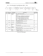
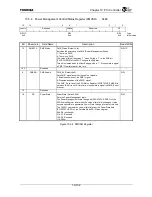
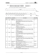
11.3.8 Reception Data Status
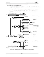
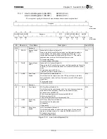
Status data such as the following is also stored in the Receive FIFO.
•
Overrun error
An overrun error is generated if all 16-stage Receive FIFO buffers become full and more data is
transferred to the Reception Read buffer. When this occurs, the Overrun Status bit is set by the last
stage of the Receive FIFO.
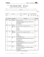
•
Parity error
A parity error is generated when a parity error is detected in the reception data.
•
Framing error
A framing error is generated when “0” is detected at the first stop bit of the reception data.
•
Break reception
A break is detected when a framing error occurs in the reception data and all data in a single
frame are “0”. When this occurs, 2 frames (2 Bytes) of 0x00 data are stored in the Receive FIFO.
Summary of Contents for TX49 TMPR4937
Page 1: ...64 Bit TX System RISC TX49 Family TMPR4937 Rev 2 0 ...
Page 4: ......
Page 13: ...Table of Contents ix TMPR4937 Revision History 1 ...
Page 14: ...Table of Contents x ...
Page 15: ...Handling Precautions ...
Page 16: ......
Page 18: ...1 Using Toshiba Semiconductors Safely 1 2 ...
Page 40: ...3 General Safety Precautions and Usage Considerations 3 18 ...
Page 42: ...4 Precautions and Usage Considerations 4 2 ...
Page 43: ...TMPR4937 2005 3 Rev 2 0 ...
Page 44: ......
Page 52: ...Chapter 1 Overview and Features 1 6 ...
Page 156: ...Chapter 7 External Bus Controller 7 56 ...
Page 491: ...Chapter 16 Removed 16 1 16 Removed ...
Page 492: ...Chapter 16 Removed 16 2 ...
Page 493: ...Chapter 17 Removed 17 1 17 Removed ...
Page 494: ...Chapter 17 Removed 17 2 ...
Page 495: ...Chapter 18 Removed 18 1 18 Removed ...
Page 496: ...Chapter 18 Removed 18 2 ...
Page 497: ...Chapter 19 Removed 19 1 19 Removed ...
Page 498: ...Chapter 19 Removed 19 2 ...
Page 506: ...Chapter 20 Extended EJTAG Interface 20 8 ...
Page 530: ...Chapter 22 Pinout and Package Information 22 10 ...
Page 542: ...Chapter 24 Parts Number when Ordering 24 2 ...

