Chapter 5 Configuration Registers
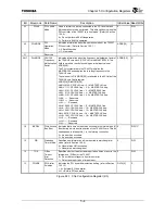
5-8
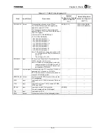
Bit
Mnemonic Field Name
Description
Initial Value Read/Write
49 DRVWE
WE Signal
Control
Specifies the driving capability of the WE
*
signal.
L : 0 = 8 mA
H : 1 = 16 mA
ADDR[5] R/W
48:45 DRVCS[3:0] SDRAM CS
Signal Control
Specifies the driving capability of the SDCS[3:0]
*
signals.
L : 0 = 8 mA
H : 1 = 16 mA
ADDR[5] R/W
44:41 DRVCK[3:0] SDRAM SDCLK
Signal Control
Specifies the driving capability of the SDCLK[3:0] signals.
L : 0 = 8 mA
H : 1 = 16 mA
ADDR[5] R/W
40 DRVCKIN
SDRAM
SDCLKIN
Signal Control
Specifies the driving capability of the SDCLKIN signal.
L : 0 = 8 mA
H : 1 = 16 mA
ADDR[5] R/W
39:33
⎯
Reserved
⎯
⎯
⎯
32
BYPASS PLL Bypass PLL
Indicates information about whether a PLL for a circuit other
than the PCI controller is on or off.
L: 0 = The PLL is off.
H: 1 = The PLL is on.
BYPASSPLL
*
R
31:30
⎯
Reserved
⎯
⎯
⎯
29:28 SDCLKDLY SDCLK
Feedback Delay
Specifies the feedback delay for the SDCLK. This function is
for diagnosis purposes. Usually, set the bits to 00.
00 = Delay 1 (minimum delay)
10 = Delay 2
01 = Delay 3
11 = Delay 4 (maximum delay)
00 R/W
27
SYSCLKEN
SYSCLK Enable Specifies whether to output the SYSCLK.
1 = Clock output
0 = H
1 R/W
26:23 SDCLKEN [3:0] SDCLK Enable Individually specifies whether to output each of SDCLK[3:0].
1 = Clock output
0 = H
Bit 26 = SDCLK[3]
Bit 25 = SDCLK[2]
Bit 24 = SDCLK[1]
Bit 23 = SDCLK[0]
1111 R/W
22 SDCLKINEN
SDCLKIN
Enable
Specifies how SDCLK[3:0] should be fed back. This function
is for diagnosis purposes. Usually, set this bit to 0.
0 = Use the SDCLKIN signal as a feedback clock.
1 = Perform feedback within the TX4937 (the SDCLKIN
becomes an output signal).
0 R/W
21:16 PCICLKEN [5:0] PCICLK Enable Individually specifies whether to output each of PCICLK[5:0].
1 = Clock output
0 = H
Bit 21 = PCICLK[5]
Bit 20 = PCICLK[4]
Bit 19 = PCICLK[3]
Bit 18 = PCICLK[2]
Bit 17 = PCICLK[1]
Bit 16 = PCICLK[0]
111111 R/W
15:10
⎯
Reserved
⎯
⎯
⎯
9 SEL2
Shared-Pin
Status 2
DMAREQ[2], DMAACK[2], and PIO[4:2] share pins with the
AC-link interface signals. Indicates which function the shared
pins are set to.
L: 0 = The shared pins are set to DMAREQ[2], DMAACK[2],
and PIO[4:2].
H: 1 = The shared pins are set to the AC-link interface signals.
ADDR[9]
R
Figure 5.2.3 Pin Configuration Register (2/3)
Summary of Contents for TX49 TMPR4937
Page 1: ...64 Bit TX System RISC TX49 Family TMPR4937 Rev 2 0 ...
Page 4: ......
Page 13: ...Table of Contents ix TMPR4937 Revision History 1 ...
Page 14: ...Table of Contents x ...
Page 15: ...Handling Precautions ...
Page 16: ......
Page 18: ...1 Using Toshiba Semiconductors Safely 1 2 ...
Page 40: ...3 General Safety Precautions and Usage Considerations 3 18 ...
Page 42: ...4 Precautions and Usage Considerations 4 2 ...
Page 43: ...TMPR4937 2005 3 Rev 2 0 ...
Page 44: ......
Page 52: ...Chapter 1 Overview and Features 1 6 ...
Page 156: ...Chapter 7 External Bus Controller 7 56 ...
Page 491: ...Chapter 16 Removed 16 1 16 Removed ...
Page 492: ...Chapter 16 Removed 16 2 ...
Page 493: ...Chapter 17 Removed 17 1 17 Removed ...
Page 494: ...Chapter 17 Removed 17 2 ...
Page 495: ...Chapter 18 Removed 18 1 18 Removed ...
Page 496: ...Chapter 18 Removed 18 2 ...
Page 497: ...Chapter 19 Removed 19 1 19 Removed ...
Page 498: ...Chapter 19 Removed 19 2 ...
Page 506: ...Chapter 20 Extended EJTAG Interface 20 8 ...
Page 530: ...Chapter 22 Pinout and Package Information 22 10 ...
Page 542: ...Chapter 24 Parts Number when Ordering 24 2 ...

