Chapter 6 Clocks
6-5
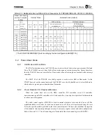
Table 6.1.4 Relationship Among Different Clock Frequencies (for TMPR4937XBG-333, CPUCLK = 333 MHz)
Master Clock (Input)
and Boot Configured
Settings
Internal Clock
External Clock (Output)
SYSCLK (MHz)
PCICLK[5:0] (MHz) †
Boot Configured Settings
PCIDIVMODE[2:0]
CCFG Settings
PCIDIVMODE[2:0]
MASTERCLK
(MHz)
Boot
Configured
Setting
ADDR[3:0]
CPUCLK
(MHz)
GBUSCLK
(MHz)
IMBUSCLK
(MHz)
SDCLK
[3:0]
(MHz)
HH
(1/1)
HL
(1/2)
LH
(1/3)
LL
(1/4)
LLH
(1/4)
LHH
(1/4.5)
HLH
(1/5)
HHH
(1/5.5)
LLL
(1/8)
LHL
(1/9)
HLL
(1/10)
HHL
(1/11)
-
HHHH(x2.0)
-
HLHH(x8.0)
-
- - - - - - - - - - - - - -
133
HHHL (x2.5)
33
HLHL (x10.0)
133 66 133
133
66
44
33
111
HHLH (x3.0)
27
HLLH (x12.0)
111 55 111
111
55
37
27
83
HHLL (x4.0)
20
HLLL (x16.0)
83 41 83
83
41
27
20
74
LHHH(x4.5)
18
LLHH (x18.0)
333
74 37 74
74
37
24
18
83 74 66 60 41 38 33 30
† The CCFG.PCIDIVMODE[2:1] field is setting by the boot configuration ADDR[11:10].
6.2 Power-Down
Mode
6.2.1
Halt Mode and Doze Mode
The WAIT instruction causes the TX49/H3 core to enter either of the two low-power modes: Halt and
Doze. The TX49/H3 can exit from Halt or Doze mode upon an interrupt exception. Ensure, therefore,
that the TX49/H3 does not enter Halt or Doze mode when all interrupts are masked in the interrupt
controller.
The HALT bit of the TX49/H3 core Config register is used to select Halt or Doze mode. As the
TX4937 does not use the snoop function of the TX49/H3 core, the bit should be set to select Halt mode,
which achieves greater power reduction than Doze mode.
6.2.2
Power Reduction for Peripheral Modules
When the system does not use the DMA controller, PCI controller, serial I/O controller,
timers/counters, parallel I/O controller, or AC-link controller, it can stop the input clock for that module
to reduce power dissipation.
The clock control register (CLKCTR) is used to control whether to turn each clock on or off. The
module should be reset before its clock can be turned on or off. This reset is performed using the reset
bit for the specific module, provided in the clock control register. The reset also initializes the registers
of the module, thus requiring subsequent setup of necessary register values and other configurations.
Refer to Section 5.2.5, "Clock Control Register" for detail of the clock control register (CLKCTR).
Summary of Contents for TX49 TMPR4937
Page 1: ...64 Bit TX System RISC TX49 Family TMPR4937 Rev 2 0 ...
Page 4: ......
Page 13: ...Table of Contents ix TMPR4937 Revision History 1 ...
Page 14: ...Table of Contents x ...
Page 15: ...Handling Precautions ...
Page 16: ......
Page 18: ...1 Using Toshiba Semiconductors Safely 1 2 ...
Page 40: ...3 General Safety Precautions and Usage Considerations 3 18 ...
Page 42: ...4 Precautions and Usage Considerations 4 2 ...
Page 43: ...TMPR4937 2005 3 Rev 2 0 ...
Page 44: ......
Page 52: ...Chapter 1 Overview and Features 1 6 ...
Page 156: ...Chapter 7 External Bus Controller 7 56 ...
Page 491: ...Chapter 16 Removed 16 1 16 Removed ...
Page 492: ...Chapter 16 Removed 16 2 ...
Page 493: ...Chapter 17 Removed 17 1 17 Removed ...
Page 494: ...Chapter 17 Removed 17 2 ...
Page 495: ...Chapter 18 Removed 18 1 18 Removed ...
Page 496: ...Chapter 18 Removed 18 2 ...
Page 497: ...Chapter 19 Removed 19 1 19 Removed ...
Page 498: ...Chapter 19 Removed 19 2 ...
Page 506: ...Chapter 20 Extended EJTAG Interface 20 8 ...
Page 530: ...Chapter 22 Pinout and Package Information 22 10 ...
Page 542: ...Chapter 24 Parts Number when Ordering 24 2 ...

