3 General Safety Precautions and Usage Considerations
3-12
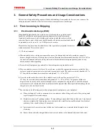
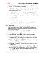
(2) If lead insertion hole intervals on the printed circuit board do not precisely match the lead pitch of the
device, do not attempt to forcibly insert devices by pressing on them or by pulling on their leads.
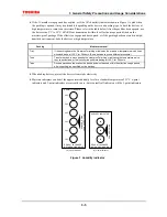
(3) For the minimum clearance specification between a device and a printed
circuit board, refer to the relevant device’s datasheet and databook. If
necessary, achieve the required clearance by forming the device’s leads
appropriately. Do not use the spacers which are used to raise devices above
the surface of the printed circuit board during soldering to achieve clearance.
These spacers normally continue to expand due to heat, even after the solder
has begun to solidify; this applies severe stress to the device.
(4) Observe the following precautions when forming the leads of a device prior to mounting.
•
Use a tool or jig to secure the lead at its base (where the lead meets the device package) while bending so as
to avoid mechanical stress to the device. Also avoid bending or stretching device leads repeatedly.
•
Be careful not to damage the lead during lead forming.
•
Follow any other precautions described in the individual datasheets and databooks for each device and
package type.
3.5.2 Socket
mounting
(1) When socket mounting devices on a printed circuit board, use sockets which match the inserted device’s
package.
(2) Use sockets whose contacts have the appropriate contact pressure. If the contact pressure is insufficient, the
socket may not make a perfect contact when the device is repeatedly inserted and removed; if the pressure
is excessively high, the device leads may be bent or damaged when they are inserted into or removed from
the socket.
(3) When soldering sockets to the printed circuit board, use sockets whose construction prevents flux from
penetrating into the contacts or which allows flux to be completely cleaned off.
(4) Make sure the coating agent applied to the printed circuit board for moisture-proofing purposes does not
stick to the socket contacts.
(5) If the device leads are severely bent by a socket as it is inserted or removed and you wish to repair the leads
so as to continue using the device, make sure that this lead correction is only performed once. Do not use
devices whose leads have been corrected more than once.
(6) If the printed circuit board with the devices mounted on it will be subjected to vibration from external
sources, use sockets which have a strong contact pressure so as to prevent the sockets and devices from
vibrating relative to one another.
Summary of Contents for TX49 TMPR4937
Page 1: ...64 Bit TX System RISC TX49 Family TMPR4937 Rev 2 0 ...
Page 4: ......
Page 13: ...Table of Contents ix TMPR4937 Revision History 1 ...
Page 14: ...Table of Contents x ...
Page 15: ...Handling Precautions ...
Page 16: ......
Page 18: ...1 Using Toshiba Semiconductors Safely 1 2 ...
Page 40: ...3 General Safety Precautions and Usage Considerations 3 18 ...
Page 42: ...4 Precautions and Usage Considerations 4 2 ...
Page 43: ...TMPR4937 2005 3 Rev 2 0 ...
Page 44: ......
Page 52: ...Chapter 1 Overview and Features 1 6 ...
Page 156: ...Chapter 7 External Bus Controller 7 56 ...
Page 491: ...Chapter 16 Removed 16 1 16 Removed ...
Page 492: ...Chapter 16 Removed 16 2 ...
Page 493: ...Chapter 17 Removed 17 1 17 Removed ...
Page 494: ...Chapter 17 Removed 17 2 ...
Page 495: ...Chapter 18 Removed 18 1 18 Removed ...
Page 496: ...Chapter 18 Removed 18 2 ...
Page 497: ...Chapter 19 Removed 19 1 19 Removed ...
Page 498: ...Chapter 19 Removed 19 2 ...
Page 506: ...Chapter 20 Extended EJTAG Interface 20 8 ...
Page 530: ...Chapter 22 Pinout and Package Information 22 10 ...
Page 542: ...Chapter 24 Parts Number when Ordering 24 2 ...


