421
Table 14.4
A/D Conversion Time (Single Mode)
CKS = 0
CKS = 1
Item
Symbol
Min
Typ
Max
Min
Typ
Max
A/D start delay
t
D
10
—
17
6
—
9
Input sampling time
t
SPL
—
64
—
—
32
—
Total A/D conversion time
t
CONV
259
—
266
131
—
134
Note:
Values are the number of states (tcyc).
14.4.4
A/D Conversion Start by External Trigger Input
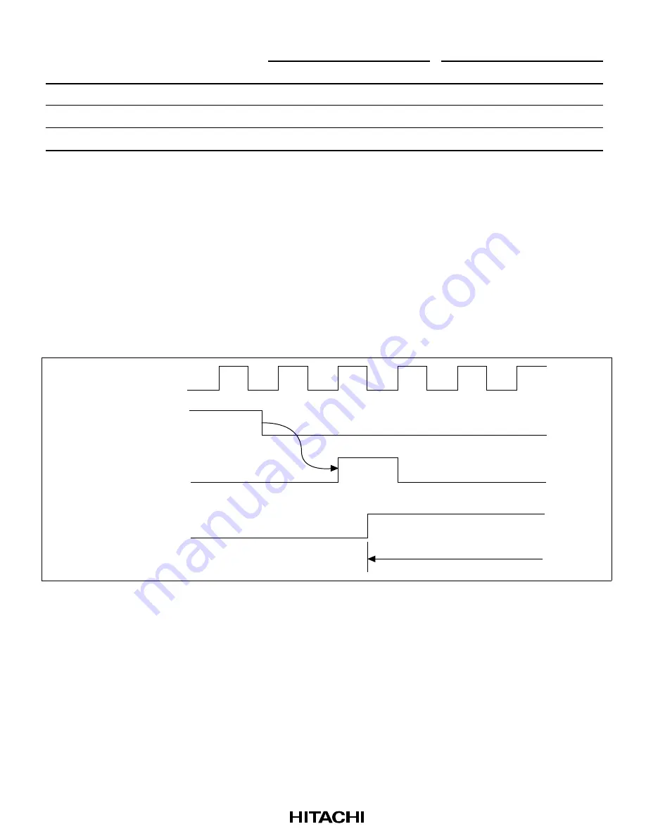
The A/D converter can be started when an external trigger is input. The external trigger is input
from the
ADTRG
input pin when the trigger enable (TRGE) bit in the A/D control register
(ADCR) is set to 1. When the
ADTRG
input pin is asserted low, the A/D start (ADST) bit in the
A/D control/status register (ADCSR) is set to 1 and A/D conversion begins. All other operations
are the same as when the ADST bit is set to 1, regardless of whether the mode is single or scan.
For the timing, see figure 14.6.
A/D conversion
CK
ADTRG
External
trigger signal
ADST
Figure 14.6 External Trigger Input Timing
14.5
Interrupts and DMA Transfer Requests
The A/D converter can generate an A/D interrupt (ADI) request at the end of conversion. The ADI
request is enabled by setting the ADIE bit in ADCSR to 1, or is disabled by clearing the bit to 0.
When ADI is generated, the DMAC can be started. DMA transfers can be performed by
requesting an ADI interrupt by setting the resource select bits (RS3–RS0) in the DMA channel
control register (CHCR) of the direct memory access controller (DMAC). The ADF bit in the A/D
control/status register (ADCSR) is automatically cleared to 0 when the DMAC accesses an A/D
converter register.
Summary of Contents for HD6417032
Page 21: ......
Page 35: ...xiv ...
Page 85: ...50 ...
Page 101: ...66 ...
Page 129: ...94 ...
Page 135: ...100 ...
Page 343: ...308 ...
Page 369: ...334 ...
Page 383: ...348 ...
Page 475: ...440 ...
Page 525: ...490 CK RAS CAS TRp TRc TRcc tRASD1 tRASD2 tCASD3 tCASD2 TRr tCSR Figure 20 18 Self Refresh ...
Page 578: ...543 CK RAS CAS TRp TRc TRcc tRASD1 tRASD2 tCASD3 tCASD2 TRr tCSR Figure 20 62 Self Refresh ...
Page 689: ...654 ...


