background image

X20 system modules  • Counter modules  • X20DC2395

796

X20 system  User's Manual 3.10

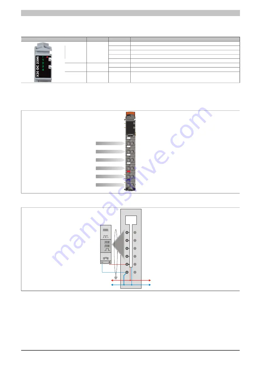
4.11.14.4 LED status indicators

For a description of the various operating modes, see the 2.11.1 "re LEDs" section.

Figure

LED

Color

Status

Description

Off

No power to module

Single flash

RESET mode

Double flash

BOOT mode (during firmware update)

1)

Blinking

PREOPERATIONAL mode

r

Green

On

RUN mode

Off

No power to module or everything OK

e

Red

On

Error or reset status

1 - 4

Green

Status of the corresponding digital signal

1)

Depending on the configuration, a firmware update can take up to several minutes.

4.11.14.5 Pinout

Shielded cables must be used for all signal lines.

X

20

 D

C

 2

39

5

Encoder 24 V +

GND

Channel 1

Channel 2

Channel 3

Channel 4

1

4

2

3

r

e

4.11.14.6 Connection example

DC

GND

+24 VDC

GND

+24 VDC

Data

Cycle

A

PWM

C

ou

nt

er

 1

Содержание X20 System

Страница 1: ...ublication however Bernecker Rainer Industrie Elektronik Ges m b H makes no warranty ex pressed or implied with regard to the products or documentation contained within this manual In addition Berneck...

Страница 2: ......

Страница 3: ...X20 CPUs 61 2 4 1 General information 61 2 4 2 Remote backplane 61 2 4 3 B R Automation Studio 62 2 4 4 PC based technology 62 2 4 5 Suitable for industrial use 62 2 5 X20 Compact CPUs 63 2 5 1 Gener...

Страница 4: ...t 90 3 8 1 Bus module rack replacement 90 3 9 X20 system infrastructure 91 3 10 Bus supply 91 3 11 Potential groups 91 3 12 Output modules with supply 92 3 13 Bus receiver with supply 92 3 14 Supply m...

Страница 5: ...e X20BR9300 113 3 24 6 3 Total internal power consumption of the X20BR9300 115 4 X20 system modules 116 4 1 Module overview Alphabetically 116 4 2 Module overview Grouped 121 4 3 Analog input modules...

Страница 6: ...93 4 3 7 3 Technical data 194 4 3 7 4 Status LEDs 196 4 3 7 5 Pin assignments 196 4 3 7 6 Connection examples 197 4 3 7 7 Input circuit diagram 197 4 3 7 8 Behavior in the event of a short circuit 197...

Страница 7: ...6 Connection example 296 4 3 13 7 Input circuit diagram 296 4 3 13 8 Register description 297 4 3 14 X20AP31x1 303 4 3 14 1 General information 303 4 3 14 2 Order data 304 4 3 14 3 Technical data 304...

Страница 8: ...n 463 4 4 6 X20AO2632 1 467 4 4 6 1 General information 467 4 4 6 2 Order data 467 4 4 6 3 Technical data 467 4 4 6 4 LED status indicators 468 4 4 6 5 Pinout 469 4 4 6 6 Connection example 469 4 4 6...

Страница 9: ...c transfer rate detection 511 4 5 2 10 Setting the transfer rate 511 4 5 2 11 Deleting parameters 512 4 5 2 12 Additional documentation and import files EDS 512 4 5 3 X20BC0043 10 513 4 5 3 1 General...

Страница 10: ...ta 537 4 5 7 3 Technical data 538 4 5 7 4 LED status indicators 539 4 5 7 5 Operating and connection elements 540 4 5 7 6 POWERLINK station number 540 4 5 7 7 RJ45 ports 541 4 5 7 8 SG3 541 4 5 7 9 SG...

Страница 11: ...ection elements 564 4 5 12 6 CAN bus interface 565 4 5 12 7 Node number and transfer rate 565 4 5 12 8 Automatic transfer rate detection 566 4 5 12 9 Setting the transfer rate 566 4 5 12 10 Save autom...

Страница 12: ...4 7 6 X20BM15 592 4 7 6 1 General information 592 4 7 6 2 Order data 592 4 7 6 3 Technical data 592 4 7 6 4 Voltage routing 593 4 7 6 5 Node number switches 593 4 7 7 X20BM21 594 4 7 7 1 General infor...

Страница 13: ...4 9 2 3 Technical data 624 4 9 2 4 LED status indicators 625 4 9 2 5 Operating and connection elements 625 4 9 2 6 Node number switches 626 4 9 2 7 Ethernet interface IF2 627 4 9 2 8 Programming the s...

Страница 14: ...t circuit diagram 656 4 11 3 8 Register description 657 4 11 4 X20DC1178 669 4 11 4 1 General information 669 4 11 4 2 Order data 669 4 11 4 3 Technical data 669 4 11 4 4 LED status indicators 671 4 1...

Страница 15: ...ription 736 4 11 10 X20DC1396 747 4 11 10 1 General information 747 4 11 10 2 Order data 747 4 11 10 3 Technical data 747 4 11 10 4 LED status indicators 749 4 11 10 5 Pinout 749 4 11 10 6 Connection...

Страница 16: ...Register description 837 4 11 16 X20DC2398 843 4 11 16 1 General information 843 4 11 16 2 Order data 843 4 11 16 3 Technical data 843 4 11 16 4 LED status indicators 845 4 11 16 5 Pinout 845 4 11 16...

Страница 17: ...elements 925 4 12 3 9 Slot for application memory 926 4 12 3 10 Operating mode switch 926 4 12 3 11 Reset button 926 4 12 3 12 CPU supply 927 4 12 3 13 RS232 interface IF1 928 4 12 3 14 Ethernet inter...

Страница 18: ...2 Order data 962 4 13 6 3 Technical data 962 4 13 6 4 Status LEDs 964 4 13 6 5 Pinout 964 4 13 6 6 Connection example 964 4 13 6 7 Input circuit diagram 965 4 13 6 8 Input filter 965 4 13 6 9 Register...

Страница 19: ...1 4 Status LEDs 1003 4 13 11 5 Pinout 1003 4 13 11 6 Connection example 1003 4 13 11 7 Input circuit diagram 1004 4 13 11 8 Input filter 1004 4 13 11 9 Register description 1005 4 13 12 X20DI6372 1007...

Страница 20: ...17 X20DI9372 1037 4 13 17 1 General Information 1037 4 13 17 2 Order data 1037 4 13 17 3 Technical data 1037 4 13 17 4 Status LEDs 1038 4 13 17 5 Pinout 1039 4 13 17 6 Connection example 1039 4 13 17...

Страница 21: ...inductive loads 1069 4 15 3 10 Register description 1070 4 15 4 X20DO2322 1074 4 15 4 1 General information 1074 4 15 4 2 Order data 1074 4 15 4 3 Technical data 1074 4 15 4 4 Status LEDs 1076 4 15 4...

Страница 22: ...r description 1116 4 15 9 X20DO4322 1120 4 15 9 1 General information 1120 4 15 9 2 Order data 1120 4 15 9 3 Technical data 1120 4 15 9 4 Status LEDs 1122 4 15 9 5 Pinout 1122 4 15 9 6 Connection exam...

Страница 23: ...Operation with inductive loads 1158 4 15 13 10 Register description 1159 4 15 14 X20DO4623 1167 4 15 14 1 General information 1167 4 15 14 2 Order data 1167 4 15 14 3 Technical data 1168 4 15 14 4 Sta...

Страница 24: ...er description 1206 4 15 19 X20DO6325 1210 4 15 19 1 General information 1210 4 15 19 2 Order data 1210 4 15 19 3 Technical data 1210 4 15 19 4 LED status indicators 1212 4 15 19 5 Pinout 1212 4 15 19...

Страница 25: ...2 Order data 1252 4 15 24 3 Technical data 1253 4 15 24 4 Status LEDs 1254 4 15 24 5 Pinout 1254 4 15 24 6 Connection example 1254 4 15 24 7 Output circuit diagram 1255 4 15 24 8 Register description...

Страница 26: ...ds 1300 4 15 29 9 Register description 1301 4 15 30 X20DOF322 1303 4 15 30 1 General information 1303 4 15 30 2 Order data 1303 4 15 30 3 Technical data 1303 4 15 30 4 Status LEDs 1305 4 15 30 5 Pinou...

Страница 27: ...5 8 Input diagram for the serial EnDat interface 1402 4 16 5 9 Encoder supply scheme and LEDs 1402 4 16 5 10 Register description 1403 4 17 Dummy modules 1453 4 17 1 Brief information 1453 4 17 2 X20...

Страница 28: ...77 4 18 6 6 Terminating resistor 1578 4 18 6 7 Register description 1579 4 18 7 X20CS1070 1617 4 18 7 1 General information 1617 4 18 7 2 Order data 1617 4 18 7 3 Technical data 1618 4 18 7 4 LED stat...

Страница 29: ...1732 4 19 5 1 General information 1732 4 19 5 2 Order data 1733 4 19 5 3 Technical data 1733 4 19 5 4 LED status indicators 1734 4 19 5 5 Operating and connection elements 1735 4 19 5 6 RJ45 ports 173...

Страница 30: ...1760 4 22 4 2 Order data 1760 4 22 4 3 Technical data 1760 4 22 4 4 Voltage routing 1761 4 22 5 X20BB47 1762 4 22 5 1 General information 1762 4 22 5 2 Order data 1762 4 22 5 3 Technical data 1762 4 2...

Страница 31: ...3 6 X20IF1051 1 1783 4 23 6 1 General information 1783 4 23 6 2 Order data 1783 4 23 6 3 Technical data 1784 4 23 6 4 LED status indicators 1785 4 23 6 5 Operating and connection elements 1785 4 23 6...

Страница 32: ...2 Order data 1805 4 23 12 3 Technical data 1806 4 23 12 4 LED status indicators 1807 4 23 12 5 Operating and connection elements 1807 4 23 12 6 PROFIBUS DP interface 1807 4 23 12 7 Firmware 1807 4 23...

Страница 33: ...ating and connection elements 1835 4 23 18 6 AS interface IF1 1835 4 23 18 7 Use with POWERLINK bus controllers 1836 4 23 18 8 Firmware 1836 4 23 19 X20IF10D1 1 1837 4 23 19 1 General information 1837...

Страница 34: ...tch positions 1859 4 23 24 7 Firmware 1859 4 23 25 X20IF2181 2 1860 4 23 25 1 General information 1860 4 23 25 2 Order data 1860 4 23 25 3 Technical data 1860 4 23 25 4 LED status indicators 1861 4 23...

Страница 35: ...1899 4 24 3 5 Operating and connection elements 1900 4 24 3 6 POWERLINK node number switches 1900 4 24 3 7 Ethernet interface 1900 4 24 3 8 Slot for hub expansion modules 1901 4 24 3 9 Usage examples...

Страница 36: ...14 Channel monitoring 1938 4 25 3 15 Overtemperature cutoff at 85 C 1938 4 25 3 16 Register description 1939 4 25 4 X20MM4331 1944 4 25 4 1 General information 1944 4 25 4 2 Order data 1944 4 25 4 3...

Страница 37: ...23 4 25 7 7 Connection options for digital inputs 2023 4 25 7 8 Input circuit diagram 2024 4 25 7 9 Output circuit diagram 2024 4 25 7 10 Overvoltage motor cutoff 2024 4 25 7 11 Overtemperature cutoff...

Страница 38: ...cators 2310 4 26 6 5 Pinout 2310 4 26 6 6 Connection example 2310 4 26 6 7 Register description 2311 4 26 7 X20PD0012 2312 4 26 7 1 General information 2312 4 26 7 2 Order data 2312 4 26 7 3 Technical...

Страница 39: ...neral information 2340 4 27 4 2 Order data 2340 4 27 4 3 Technical data 2340 4 27 4 4 LED status indicators 2341 4 27 4 5 Pinout 2342 4 27 4 6 Connection examples 2342 4 27 4 7 Derating 2343 4 27 4 8...

Страница 40: ...5 3 Technical data 2377 4 29 5 4 LED status indicators 2378 4 29 5 5 Operating and connection elements 2378 4 29 5 6 Ethernet interface 2378 4 29 6 X20PS8002 2379 4 29 6 1 General information 2379 4...

Страница 41: ...circuit diagram 2412 4 31 5 8 Register description 2413 4 31 6 X20ATA492 2420 4 31 6 1 General information 2420 4 31 6 2 Order data 2420 4 31 6 3 Technical data 2420 4 31 6 4 Status LEDs 2423 4 31 6...

Страница 42: ...view Grouped 2486 5 3 Analog input modules 2488 5 3 1 Brief information 2488 5 3 2 X20cAI2438 2489 5 3 2 1 General information 2489 5 3 2 2 Order data 2489 5 3 2 3 Technical data 2490 5 3 3 X20cAI4622...

Страница 43: ...a 2520 5 5 4 3 Technical data 2521 5 6 Bus controllers System modules 2522 5 6 1 Brief information 2522 5 6 2 X20cBB80 2523 5 6 2 1 General information 2523 5 6 2 2 Order data 2523 5 6 2 3 Technical d...

Страница 44: ...0 X20 CPUs 2551 5 10 1 Brief information 2551 5 10 2 X20cCPx58x 2552 5 10 2 1 General information 2552 5 10 2 2 Order data 2552 5 10 2 3 Technical data 2552 5 11 Digital input modules 2556 5 11 1 Brie...

Страница 45: ...ion 2581 5 13 6 2 Order data 2581 5 13 6 3 Technical data 2581 5 13 7 X20cDO9322 2583 5 13 7 1 General information 2583 5 13 7 2 Order data 2583 5 13 7 3 Technical data 2583 5 14 Digital signal proces...

Страница 46: ...information 2610 5 20 2 X20cIF1030 2611 5 20 2 1 General information 2611 5 20 2 2 Order data 2611 5 20 2 3 Technical data 2612 5 20 3 X20cIF1061 1 2613 5 20 3 1 General information 2613 5 20 3 2 Ord...

Страница 47: ...n 2639 5 23 2 X20cHB8884 2640 5 23 2 1 General information 2640 5 23 2 2 Order data 2640 5 23 2 3 Technical data 2641 5 24 System modules for the X20 hub system 2642 5 24 1 Brief information 2642 5 24...

Страница 48: ...nical handling 2667 7 1 Solid mechanics 2667 7 2 Number of connection cycles 2667 7 3 Assembling an X20 system 2668 7 3 1 Variant 1 2669 7 3 2 Variant 2 2672 7 4 Installing the X20 system on the top h...

Страница 49: ...Table of contents X20 system User s Manual 3 10 49 B 3 B R ID codes sorted by model number 2698...

Страница 50: ...ectronics module communication Motor modules Other modules Temperature modules Counter modules The most up to date data sheets for the respective modules can be downloaded from the B R website 2 10 Ma...

Страница 51: ...CPUs Fieldbus CPU system modules Communication in the X20 IF module X20 electronics module communication Digital mixed modules Other modules Existing module groups updated Bus modules Terminal blocks...

Страница 52: ...or comparable product or Slot PLC e g B R LS251 or comparable product safety precautions relevant to industrial control systems e g the provision of safety devices such as emergency stop circuits etc...

Страница 53: ...d under Electrical components with a housing Any persons handling electrical components or devices with installed electrical components must be grounded Components are only permitted to be touched on...

Страница 54: ...s Devices are only permitted to be installed by qualified personnel without voltage applied General safety guidelines and national accident prevention regulations must be observed Electrical installat...

Страница 55: ...1 2 7 Environmentally friendly disposal All B R control components are designed to inflict as little harm on the environment as possible 1 2 7 1 Separation of materials It is necessary to separate di...

Страница 56: ...PP35 PP41 SG4 System Generation 4 SG4 CPUs with Intel processors The following CPUs belong to this series CP1583 CP1584 CP1585 CP1586 CP3583 CP3584 CP3585 CP3586 CP1483 CP1483 1 CP340 CP360 CP380 CP38...

Страница 57: ...ree basic elements Terminal block Electronic module Bus module 2 1 1 More than just I O With its well thought out details and a sophisticated ergonomic design the X20 system is more than a remote I O...

Страница 58: ...implest usability The X20 system delivers 50 more component density perfected connection technology and optimal gran ularity Added value 12 channels with a width of 12 5 mm allow a component density n...

Страница 59: ...ible to pre wire the entire control cabinet This is especially ideal for series produced machines Easy maintenance X20 modules can be easily exchanged to simplify troubleshooting The electronic module...

Страница 60: ...cables This not only provides a universal remote backplane which handles the communication between bus modules and via the X2X Link cable but makes it possible without converters or any loss in perfo...

Страница 61: ...ations there are also up to three multipurpose slots for additional interface modules Because the X20 CPU was designed for top hat rail installation in a control cabinet up to 250 X20 I O modules 3000...

Страница 62: ...RAM for task specific data and remanent variables In the case of a power failure variables that have been declared as being remanent are automatically copied from the fast RAM to the secure SRAM Data...

Страница 63: ...hese are attached seamlessly to the CPU making the entire system an extreme space saver in the control cabinet Despite the sleek profile the CPU supply the X2X Link supply and the I O module supply ar...

Страница 64: ...e full CPU functionality of the Compact CPUs plus a plug in fieldbus module create many more possibilities than simply data preprocessing There are enough reserves for relatively complex application p...

Страница 65: ...le a bus controller allows the X20 system to be used as a powerful I O expansion unit Standardized EDS or GSD description files allow X20 system components to be integrated configured and programmed i...

Страница 66: ...and manufacturer independent control of valve terminals A complete digital output module in a size and form comparable with a normal DSUB connector XV allows any valve terminal manufacturer to be sele...

Страница 67: ...provides many advantages for control cab inet construction Separate manufacturing just in time logistics and the installation of preassembled systems during start up become reality Tool free Simple to...

Страница 68: ...ail with the same ease as a rack system They also make it just as simple to remove it from the rail The sophisticated mechanics of the X20 are needed not just to provide this type of handling but also...

Страница 69: ...ge With the X20 system status data does not result in an additional communication load which would result in considerable differences between theoretically possible bus speeds and real requirements du...

Страница 70: ...nding on the configuration a firmware transfer can take several minutes Blinking Off PREOPERATIONAL mode Modules whose slot is configured for a different module or none at all remain in PREOPERATIONAL...

Страница 71: ...created optimally according to the actual requirements However the application software is designed to handle all potential options Only the I O channels that are actually available are configured in...

Страница 72: ...cases e g when configurations of modular machines change it is necessary to define specific module groups at a fixed address regardless of the preceding modules in the line For this purpose there are...

Страница 73: ...ns Integrated supply and ground for sensors and actu ators GND 24 VDC GND 24 VDC DI Sensor 1 Sensor 2 Universal 2 wire connections No extra terminals needed GND 24 VDC GND 24 VDC DI Sensor 5 Sensor 3...

Страница 74: ...bsite www br automation com For a description of the redundant X2X Link supply see section 3 20 X2X Link supply 2 19 reACTION technology The X20 Compact CPUs and a number of I O modules are available...

Страница 75: ...de with a bus transmitter Supply modules and I O modules are placed between the bus receiver or bus controller and the bus transmitter as needed The power supply system used in the X20 systems is desc...

Страница 76: ...3rd party development environment Power supply module X20PS211x For internal I O supply Supply bus module X20BM01 I O modules Standard bus module X20BM11 Power supply module X20PS331x For X2X Link and...

Страница 77: ...s receiver X20BR9300 Supply bus module X20BM01 Power supply module X20PS211x For internal I O supply Supply bus module X20BM01 I O modules Standard bus module X20BM11 Power supply module X20PS331x For...

Страница 78: ...l and electrical configuration 3 1 Dimensions 3 1 1 X20 CPUs with one slot for interface modules 150 0 2 99 85 Figure 16 Dimensions of the X20 CPUs with one slot 3 1 2 X20 CPUs with three slots for in...

Страница 79: ...PUs and bus controllers 3 1 4 Fieldbus CPUs and expandable bus controller 3 1 4 1 With an additional slot 62 5 0 2 99 75 Figure 19 Dimensions of the fieldbus CPUs and expandable bus controller with on...

Страница 80: ...75 Figure 21 Dimensions of the I O modules 3 1 6 CAD support To ensure CAD support the dimensions are included in the ECAD macros in 2D STEP data is available to allow 3D viewing The STEP data can be...

Страница 81: ...automatically applied by the configuration and programming system Automation Studio Design and changes are immediately reflected at all levels of development This saves time for the more important ta...

Страница 82: ...n and locked in place by closing the unlocking mechanisms Finally the modules are equipped with the prewired terminal blocks Information Only horizontal or vertical mounting orientation is permitted 3...

Страница 83: ...to the left of the modules Above and below the X20 system there must be at least 10 mm of free space To the right of the modules 35 mm space must be left free for I O and power supply cabling The mod...

Страница 84: ...secure connection Information The wire stripping length must not be more or less than 7 to 9 mm 3 5 Stress relief using cable ties Figure 25 Stress relief using cable ties The X20 system terminal bloc...

Страница 85: ...elines apply for shielding The X20 top hat rail must always be mounted to a conductive backplane Shielded cables must be grounded on both sides 3 6 1 Direct shielding connection The shield is twisted...

Страница 86: ...is latched to the terminal block and connected to the bus module s ground connection using a cable lug Cable ties are used to press the shield against the grounding plate Figure 28 Shielding via X20 c...

Страница 87: ...using ground terminals from another manufacturer e g PHOENIX or WAGO or a cable tie Attaching the shield with a ground terminal Attaching the shield with a cable tie Cable duct Cable duct Table 5 Cabl...

Страница 88: ...ng terminal via the top hat rail to connect the X2X Link cable shield directly with the conductive and grounded backplane This will generally exceed the specified EMC minimal requirements The shielded...

Страница 89: ...INK cable with RJ45 connector The following wiring guidelines must be observed Use CAT5 SFTP cables Observe minimum cable flex radius see data sheet for the cable Secure the cable underneath the bus c...

Страница 90: ...supply contacts Bus data contacts I O supply contacts X20BM11 X20BM01 Figure 31 The bus module replaces the rack in the X20 system The bus module is the backbone of the X20 system regarding the bus s...

Страница 91: ...electrically isolated the X2X Link supply needs to be fed in at certain intervals This is initially handled by the bus receiver A supply module for X2X Link must be added to refresh the supply after...

Страница 92: ...he X2X Link is fed by the X20BR9300 bus receiver After approx 30 modules see section 3 23 Calculating the power requirements for a calculation example the supply must be refreshed The X20PS3300 power...

Страница 93: ...1 A slow blow 1 PS2100 BM01 I O 10 A slow blow PS2100 BM01 Figure 33 Protecting various potential groups 1 Recommended for line protection 3 19 2 Supply via bus transmitter The bus transmitter has an...

Страница 94: ...e backplane even if the X2X Link supply fails Please note the following for the correct calculation To determine the necessary X2X Link power calculate using 75 of the power supply module s rated powe...

Страница 95: ...s U1 24 VDC U2 24 VDC X2X Link X2X Link X2X Link I O I O I O BR9300 BM01 PS3300 BM01 PS3300 BM01 10 A slow blow 10 A slow blow 1 A slow blow 1 1 A slow blow 1 1 A slow blow 1 10 A slow blow 2 Figure 3...

Страница 96: ...ese guidelines are met B R will not assume warranty or liability for damages that occur due to Improper use Non observance of standards and guidelines Unauthorized modifications to devices connections...

Страница 97: ...H0 X20DS1119 X20 multifunctional digital signal processor 3 digital channels 5 V symmetric configurable as inputs or outputs 2 digital input channels 24 V asymmetric max 2 event counters 1 univer sal...

Страница 98: ...tual duration of cutoff can be calculated with the following formula tspec Actual cutoff time Ctot Total capacity of all modules in the potential group e g 10 modules 47 F 3 modules with 150 F Ctot 92...

Страница 99: ...For modules with isolated I O potential for sensors and actuators the upstream safety relay must shut off the supply for both the sensors and actuators otherwise energy regeneration cannot be exclude...

Страница 100: ...Reference potential for GND potential group 0 VDC inputs and outputs Power supply for 24 VDC potential group inputs and outputs Load Figure 39 Circuit example 2 Two channel with feedback Provided that...

Страница 101: ...vice Make sure that ALL of the potential group s input and output channels and the connected sensors and actuators are wired properly A short circuit between an input or output of the potential group...

Страница 102: ...es When using the operating principle with uncoated X20 modules the modules must not be op erated in condensing relative humidity or with ambient temperatures below 0 C It is not permitted to mix modu...

Страница 103: ...Link Open cables X67CA0X41 xxxx X67CA0X51 xxxx X2X Link Attachment cable X67CA0X21 xxxx X67CA0X31 xxxx X67PS1300 X67 I O X67 I O X67 I O Compact I O system 24 V 24 V X2X Link Open cables X67CA0X41 xx...

Страница 104: ...ut Out Out X2X optional 1 X2X optional 1 X2X X2X X2X X2X X2X X2X Shield 24 VDC supply Shield Supply Blue White Black Blue White Black 1 Used to forward the X2X Link supply when using IP67 modules Sign...

Страница 105: ...ink in out Cable for custom assembly 100 m X67CA0X99 1000 Table 10 Connection example for valve connection 7XVxxx xx 11 12 1 In connection with X67 modules Connection example with 7XVxxx xx 21 1 3 4 5...

Страница 106: ...ion is provided by the power supply modules the X20 CPU the bus receivers and the bus transmitters Module I O internal power Bus power X20CP148x X20CP158x X20CP358x 240 W 7 W X20BR9300 240 W 7 W X20PS...

Страница 107: ...configuration Module Bus power W I O internal power W I O external power W Sensor Actuator supply W 1 X20DI4371 0 14 0 59 12 00 X20DI2371 0 12 0 29 12 00 X20DO4322 0 16 0 49 48 002 12 00 X20DO4322 0...

Страница 108: ...12 00 1 Rated power at 24 VDC and 100 simultaneity 2 Rated power at 24 VDC and 0 5 A 3 The power supply is integrated in the module Potential group 3 Module Bus power W I O internal power W I O extern...

Страница 109: ...Power requirements of all bus modules 1 82 Remaining power 3 96 225 42 1 Rated power at 24 VDC and 10 A 2 Bus power to be supplied for all I O modules i e sum of the bus power of all potential groups...

Страница 110: ...ctiveness of the power supplies The data sheets for the power supply modules list their own power requirements and power loss as maximum power consumption With the formulas in the following sections t...

Страница 111: ...supply modules with X2X Link supply PX2X Sum of the bus power consumption of all modules in the X20 system compact CPU fieldbus CPU BC BR I O BM BT n Number of all power supply modules in the X20 sys...

Страница 112: ...Bus power consumption of all modules in the X20 system The sum of the bus power consumption from all of the modules in the X20 system is necessary in order to calculate the internal X2X Link power co...

Страница 113: ...urrents Internal power consumption of the I O modules The current that results from the internal consumption of the I O modules is calculated according to the following formula Sum of output and actua...

Страница 114: ...0 1 A Figure 46 Connections and currents of the second X20DO4322 Calculating the sum of the output currents Calculating the sum of the actuator currents Calculating the I O summation current The I O s...

Страница 115: ...nd currents of the second X20DO4322 GND 24 VDC GND 24 VDC DO Actuator 1 Actuator 2 Actuator 3 0 45 A 0 35 A 0 07 A 0 09 A 0 5 A 0 1 A Figure 47 Connections and currents of the second X20DO4322 Calcula...

Страница 116: ...t power energy calculates root mean square values 240 V keyed 304 X20AP3121 X20 energy measurement module 3 analog inputs 480 VAC 50 60 Hz 4 analog inputs 1 A AC calculates effective reactive and appa...

Страница 117: ...le 240 V coded internal I O supply is interconnected 590 X20BM15 X20 bus module with node number switches internal I O supply is interconnected 592 X20BM21 X20 bus module for double width modules inte...

Страница 118: ...653 X20DC1178 X20 digital counter module 1 SSI absolute encoders 5 V 1 MBit s 32 bit encoder monitoring NetTime module 669 X20DC1196 X20 digital counter module 1 ABR incremental encoders 5 V 600 kHz...

Страница 119: ...ule 1x EnDat 2 1 2 2 NetTime module 1399 X20DS438A X20 digital signal module 4x I O Link master V1 1 can also be configured as 4x digital input or output channels 3 wire connections 2244 X20ET8819 X20...

Страница 120: ...D0012 X20 potential distributor module 12x 24 VDC integrated microfuse 2312 X20PD0016 X20 potential distributor module 5x GND 5x 24 VDC floating feed integrated microfuse 2316 X20PD2113 X20 potential...

Страница 121: ...memory CompactFlash 3 insert slots for X20 interface modules 2 USB interfaces 1 RS232 interface 1 Ethernet inter face 10 100 1000 Base T 1 POWERLINK interface incl supply module 1 X20TB12 terminal bl...

Страница 122: ...20AO2632 1 X20 analog output module 2 outputs 11 V 0 to 22 mA 16 bit resolution 467 X20AO4622 X20 analog output module 4 outputs 10 V 0 to 20 mA 4 to 20 mA 13 bit resolution 474 X20AO4632 X20 analog o...

Страница 123: ...source configurable input filter 3 wire connections 942 X20DI2377 X20 digital input module 2 inputs 24 VDC sink configurable input filter 2 event counters 50 kHz 3 wire connections 948 X20DI2653 X20...

Страница 124: ...rding to fieldbus CPU base order power supply module bus base and terminal block separately 1748 X20XC0202 X20 CPU fieldbus CPU P 25 750 kB SRAM 3 MB FlashPROM support of RS232 CAN and interface modul...

Страница 125: ...b expansion module integrated 1x hub 1 fiber optic connection 2367 X20HB2880 X20 hub expansion module 2x RJ45 2370 X20HB2881 X20 hub expansion module integrated 2x hub for fiber optic connection 2373...

Страница 126: ...0IF1020 X20 interface module 1 RS232 max 115 2 kbit s electrically isolated 1769 X20IF1030 X20 interface module 1 RS422 RS485 max 115 2 kbit s electrically isolated 1772 X20IF1041 1 X20 interface modu...

Страница 127: ...iew Grouped X20 system User s Manual 3 10 127 Product ID Short description on page X20 redundancy systems X20HB8884 X20 compact link selector 2x RJ45 connection order bus base power supply module and...

Страница 128: ...mA 16 bit resolution each channel electrically isolated and with own sensor supply HART protocol supported 193 X20AI2622 X20 analog input module 2 inputs 10 V or 0 to 20 mA 4 to 20 mA 13 bit resoluti...

Страница 129: ...set from 2 5 Hz to 7 5 kHz Special operating modes synchronous mode and multiple sampling 4 3 2 2 Order data Model number Short description Figure Analog input modules X20AI1744 X20 analog input modu...

Страница 130: ...ital value Broken bridge supply line Value approaches 0 Broken sensor line Value approaches end value Status bit open circuit in register Module status is set Valid value range 0x007FFFFF to 0xFF80000...

Страница 131: ...Ds The status LEDs are identical on the X20AI1744 and X20AI1744 3 modules Image LED Color Status Description Off No power to module Single flash Reset mode Double flash Boot mode during firmware updat...

Страница 132: ...bypassed by the 4 internally linked strain gauge VCC connections i e strain gauge GND For this reason the line compensation no longer functions The measurement precision is therefore affected by chan...

Страница 133: ...4 VDC AI Full bridge strain gauge 1 U Full bridge strain gauge 2 U Figure 51 Connection example Parallel connection of 2 full bridge strain gauges When connecting 3 or more full bridge strain gauges i...

Страница 134: ...ution is always less than 24 bit This effective resolution depends on the data rate and measurement range Example Because of the conversion methods a data rate of 2 5 Hz and a specified measurement ar...

Страница 135: ...ight to the converter value and vice versa This simplified theoretical approach is only valid for an ideal mea surement system Calibration of the entire measurement system is recommended because not o...

Страница 136: ...e number of measured values should not exceed the number of measurements that can actually be made All other measured values are invalid 0x8000 To minimize the load on X2X Link it is possible to disab...

Страница 137: ...surement range see Effective resolution of the AD converter The following table shows how the effective resolution in bits or the effective value range of the strain gauge value depend on the module c...

Страница 138: ...40 000 17 8 114 000 17 66 000 3750 18 1 140 000 17 8 114 000 17 3 81 000 16 6 50 000 7500 17 7 106 000 17 3 81 000 16 9 61 000 16 2 38 000 Table 23 Effective resolution of the strain gauge value in bi...

Страница 139: ...g time Jitter ADC cycle times 1500 s ADC cycle times 1500 s Max 1 s Max 4 s Dead time on the X2X Link 50 s X2X cycle time 128 Settling time Firmware Version Firmware Version 5 Max 150 x ADC cycle time...

Страница 140: ...ed on the serial number 50 10000 505 49 9800 504 9 2 400 500 2 1 200 500 1 0 0 500 1 200 499 9 2 400 499 8 50 10000 495 51 SerialNo modulo 100 50 200 ppm Based on the serial number 128 SerialNo modulo...

Страница 141: ...er contains the raw value determined by the ADC for the full bridge strain gauge with 16 bit resolution The module returns between 3 and 10 measured values per X2X cycle depending on the configuration...

Страница 142: ...rk reliably because of the variable input impedance of the amplifier in relation to the set data rate 4 3 2 11 5 4 ADC cycle time Name ConfigCycletime1_MultiSample This register can be used to configu...

Страница 143: ...le for handling monitoring diagnostics and acyclic commands Minimum cycle time 250 s 4 3 2 11 7 Minimum I O update time The minimum I O update time defines how far the bus cycle can be reduced while s...

Страница 144: ...C keyed X20TB12 X20 terminal block 12 pin 24 VDC keyed Table 28 X20AI2222 Order data 4 3 3 3 Technical data Product ID X20AI2222 Short description I O module 2 analog inputs 10 V General information B...

Страница 145: ...orizontal installation 25 to 60 C Vertical installation 25 to 50 C Derating Storage 40 to 85 C Transport 40 to 85 C Relative humidity Operation 5 to 95 non condensing Storage 5 to 95 non condensing Tr...

Страница 146: ...s Manual 3 10 4 3 3 5 Pinout AI 1 U AI 1 U AI 2 U AI 2 U X20 AI 2222 r 1 e 2 Figure 54 Pinout 4 3 3 6 Connection example GND 24 VDC GND 24 VDC AI 4 3 3 7 Input circuit diagram AI x U AI x U A D Conve...

Страница 147: ...ycle and transferred in the same cycle 4 3 3 8 4 Analog input values Name AnalogInput01 to AnalogInput02 The analog input values are mapped to this register Data type Value Input signal INT 32 768 to...

Страница 148: ...th the following settings Input ramp limitation 4 0x07FF 2047 Filter level 2 0 8000 17000 t ms Input jump 1 2 3 4 5 6 7 8 Input value Internally adjusted input value before filtering Figure 56 Adjuste...

Страница 149: ...ter level Adjustable filter levels Value Filter level 0 Filter switched off 1 Filter level 2 2 Filter level 4 3 Filter level 8 4 Filter level 16 5 Filter level 32 6 Filter level 64 7 Filter level 128...

Страница 150: ...1 Filter level 2 010 Filter level 4 011 Filter level 8 100 Filter level 16 101 Filter level 32 110 Filter level 64 0 2 Defines the filter level 111 Filter level 128 3 Reserved 0 000 The input value is...

Страница 151: ...Upper limit value exceeded 2 3 Channel 2 11 Open line 4 7 Reserved 0 Limiting the analog value In addition to the status information the analog value is set to the values listed below by default when...

Страница 152: ...Terminal blocks X20TB12 X20 terminal block 12 pin 24 VDC keyed Table 31 X20AI2237 Order data 4 3 4 3 Technical data Product ID X20AI2237 Short description I O module 2 analog inputs 10 V General info...

Страница 153: ...rical isolation Sensor supply Channel No Sensor supply Sensor supply Yes Maximum voltage ripple Up to 100 kHz 2 2 mV Up to 1 MHz 22 mV higher 100 mV Short circuit current Typical 50 mA Maximum 60 mA B...

Страница 154: ...onnected or overload V Yellow On Sensor supply in its normal operating range Analog input Off Indicates one of the following cases Module supply not connected Channel disabled Open line Single flash I...

Страница 155: ...source GND 24 VDC GND 24 VDC AI Voltage source 2 wire Transducer passive 4 3 4 6 2 4 wire connection A 4 wire connection can be implemented as follows 4 wire transducer with external supply 4 wire tr...

Страница 156: ...erter 25 V DC DC 28 V DC DC 5 V Electrical Isolation I O Supply 18 30 V DC DC 3 3 V Input filter GND x GND x GND I O 4 3 4 8 Behavior in the event of a short circuit In the event of a short circuit th...

Страница 157: ...lacementUpper02 INT 410 454 ReplacementLower01 ReplacementLower02 INT 426 470 PreparationInterval01 PreparationInterval02 UINT 418 462 ErrorDelay01 ErrorDelay02 UINT 422 466 SumErrorDelay01 SumErrorDe...

Страница 158: ...2 INT 406 450 Hysteres01 Hysteres02 INT 414 458 ReplacementUpper01 ReplacementUpper02 INT 410 454 ReplacementLower01 ReplacementLower02 INT 426 470 PreparationInterval01 PreparationInterval02 UINT 418...

Страница 159: ...cally impermissible voltage value or an open line is detected the limit monitor triggers an appropriate response The response is determined by the replacement value strategy selected by the user With...

Страница 160: ...w the evaluated input value behaves during normal operation Configured filter level 2 or 4 Jump in incoming raw value From 8000 to 16000 0 8000 16000 t 1 0 2 3 4 5 6 7 8 Raw value jump Evaluated value...

Страница 161: ...ated input value behaves during normal operation Input limitation 2047 Configured filter level 2 Jump in incoming raw value From 8000 to 17000 0 8000 17000 t 1 2 3 4 5 6 7 8 Raw value jump Evaluated v...

Страница 162: ...4 9 4 2 AnalogMode Name AnalogMode01 AnalogMode02 These registers are used to predefine the operating parameters that the module will be using for the respective channel Each channel must be enabled i...

Страница 163: ...being used then a hysteresis range should also be defined The Hysteresis registers configure how far a limit value can be exceeded before a response is triggered The error status is cleared when the...

Страница 164: ...interval If a permis sible value is present then the contents of the buffer memory are passed to output memory and the contents of the measurement value memory are passed to the buffer If the check tu...

Страница 165: ...ment value strategy Some error information may be delayed according to the previously configured condition Data type Values USINT See bit structure Bit structure Bit Name Value Note 0 Value equals low...

Страница 166: ...cessed on the module during each cycle and transferred cyclically via the bus In this way it is possible to minimize the cycle time by selecting the correct function model Function model Number Automa...

Страница 167: ...l block 6 pin 24 VDC keyed X20TB12 X20 terminal block 12 pin 24 VDC keyed Table 35 X20AI2322 Order data 4 3 5 3 Technical data Product ID X20AI2322 Short description I O module 2 analog inputs 0 to 20...

Страница 168: ...uction of ambient temperature by 0 5 C per 100 m EN 60529 protection IP20 Environmental conditions Temperature Operation Horizontal installation 25 to 60 C Vertical installation 25 to 50 C Derating St...

Страница 169: ...3 10 169 4 3 5 5 Pinout AI 1 I AI 1 I AI 2 I AI 2 I X20 AI 2322 r 1 e 2 Figure 65 Pinout 4 3 5 6 Connection example GND 24 VDC GND 24 VDC AI 4 3 5 7 Input circuit diagram PTC Shunt AI x I AI x I A D...

Страница 170: ...et to the network cycle and transferred in the same cycle 4 3 5 8 4 Analog input values Name AnalogInput01 to AnalogInput02 The analog input values are mapped to this register Data type Value Input si...

Страница 171: ...th the following settings Input ramp limitation 4 0x07FF 2047 Filter level 2 0 8000 17000 t ms Input jump 1 2 3 4 5 6 7 8 Input value Internally adjusted input value before filtering Figure 67 Adjuste...

Страница 172: ...ter level Adjustable filter levels Value Filter level 0 Filter switched off 1 Filter level 2 2 Filter level 4 3 Filter level 8 4 Filter level 16 5 Filter level 32 6 Filter level 64 7 Filter level 128...

Страница 173: ...1 This register is used to define the filter level and input ramp limitation of the input filter Data type Value USINT See bit structure Bit structure Bit Description Value Information 000 Filter swit...

Страница 174: ...t03 This register can be used to configure the lower limit for analog values If the analog value goes below the limit value it is frozen at this value and the corresponding error status bit is set Dat...

Страница 175: ...occurs The analog value is limited to the new values if the limit values were changed Digital value for error default values Error status 0 to 20 mA 4 to 20 mA Upper limit value exceeded 32767 0x7FFF...

Страница 176: ...n the two measurement ranges 4 to 20 mA and 0 to 25 mA 2 analog current measurement inputs Electrically isolated analog channels Electrically isolated sensor supplies 16 bit digital converter resoluti...

Страница 177: ...Output format 4 to 20 mA INT 0000 7FFF 1 LSB 0001 488 281 nA 0 to 25 mA INT 0000 7FFF 1 LSB 0001 762 939 nA 0 to 25000 A INT 0000 61A8 1 LSB 0001 1000 nA Load 300 Input protection Up to 30 VDC reverse...

Страница 178: ...2 5 0 2 mm Table 39 X20AI2437 Technical data 1 To reduce power dissipation B R recommends leaving unused inputs open 2 Sensor supply 3 Based on the current measurement value 4 Based on the 25 mA measu...

Страница 179: ...ction examples 4 3 6 7 Input circuit diagram Shunt Sensor supply x Sensor supply x Channel x Channel x A D Converter Processor Protection and Filter Input protection Output protection DC DC Converter...

Страница 180: ...6 PreparationInterval_1 UINT 414 ReplacementUpper_1 INT UINT 410 ReplacementLower_1 INT UINT 402 UpperLimit_1 INT UINT 398 LowerLimit_1 INT UINT 406 Hysteres_1 INT UINT 418 ErrorDelay_1 UINT 422 SumEr...

Страница 181: ...L OpenLineAnalogInput01 BOOL ConversionErrorAnalogInput01 BOOL SumErrorAnalogInput01 BOOL SensorErrorAnalogInput01 BOOL IoSuppErrorAnalogInput01 BOOL AnalogInput01 INT UINT AnalogSampletime01 INT UINT...

Страница 182: ...onInterval_1 UINT 414 ReplacementUpper_1 INT UINT 410 ReplacementLower_1 INT UINT 402 UpperLimit_1 INT UINT 398 LowerLimit_1 INT UINT 406 Hysteres_1 INT UINT 418 ErrorDelay_1 UINT 422 SumErrorDelay_1...

Страница 183: ...OverflowAnalogInput01 BOOL OpenLineAnalogInput01 BOOL ConversionErrorAnalogInput01 BOOL SumErrorAnalogInput01 BOOL SensorErrorAnalogInput01 BOOL IoSuppErrorAnalogInput01 BOOL AnalogInput01 INT UINT C...

Страница 184: ...aluated input values The configured auxiliary functions are applied to form these values Data type Values 0 25000 Normalizing option 0 to 25 mA 0 32767 Normalizing option 0 to 25 mA INT 0 32767 Normal...

Страница 185: ...0x 0 No error 4 Composite error 1 Composite error on Channel 0x 5 Reserved 0 No error 6 Sensor error 1 Sensor error on Channel 0x 0 No error 7 I O supply error 1 I O supply error on Channel 0x Data po...

Страница 186: ...the configurable delay time has passed ErrorDelay registers Conversion error This error status is triggered when the hardware exceeds the conversion time Composite error This error information derive...

Страница 187: ...us controller default setting 0 Underflow detection turned off 2 Underflow detection 1 Underflow detection enabled bus controller default setting 0 Use replacement values when an error occurs bus cont...

Страница 188: ...hey do not meet the specifications When an error does not occur therefore the measurement value acquired two preparation intervals ago is constantly output Data type Values 0 1 ms UINT 0 65535 Applica...

Страница 189: ...g input taking the configured normalization into account as well When an overflow or underflow error status occurs the AnalogInputEvaluated0x channel is replaced with the corresponding value Using a d...

Страница 190: ...ue A 1 31068 5242 72 1 5625 Displaying 0 25 mA as 0 65535 55049 limit value A 65535 25000 LowerLimit Displaying 0 25 mA as 0 25000 3600 Displaying 0 25 mA as 0 32767 4718 limit value A 32767 25000 Dis...

Страница 191: ...to underflow overflow and open circuit errors This delay can be used to hide temporary measurement value deviations for example Data type Values UINT 0 10 Error formation delay conversion cycles 2 co...

Страница 192: ...via the bus In this way it is possible to minimize the cycle time by selecting the correct function model 4 3 6 9 8 Minimum cycle time The minimum cycle time defines how far the bus cycle can be redu...

Страница 193: ...ect between the two measurement ranges 4 to 20 mA and 0 to 25 mA 2 analog current measurement inputs HART protocol integration Support for HART variables Electrically isolated analog channels Electric...

Страница 194: ...ut rate With HART 4 7 to 10 scans per second can be set using software Analog 4 7 to 100 scans per second can be set using software Output format INT Output format 4 to 20 mA INT 0x0000 0x7FFF 1 LSB 0...

Страница 195: ...um 800 mVpp Operating conditions Mounting orientation Horizontal Yes Vertical Yes Installation at altitudes above sea level 0 to 2000 m No limitations 2000 m Reduction of ambient temperature by 0 5 C...

Страница 196: ...el disabled Open line Single flash Input signal overflow or underflow Double flash A conversion error has occurred A single flash is output on the red e module status LED 1 2 Green On Analog digital c...

Страница 197: ...TS Request to Send Output protection DC DC Converter 25 V DC DC 28 V DC DC 3 3 V Electrical Isolation I O Supply 18 30 V Shunt GND x GND x GND I O GND x 4 3 7 8 Behavior in the event of a short circui...

Страница 198: ...er_1 INT UINT 402 UpperLimit_1 INT UINT 398 LowerLimit_1 INT UINT 406 Hysteres_1 INT UINT 418 ErrorDelay_1 UINT 422 SumErrorDelay_1 UINT Analog signal Configuration channel 02 426 AnMode_2 UINT 430 Sa...

Страница 199: ...38 PvCountHartRxError01 UINT 546 PvCountHartFrameError01 UINT 554 PvNodeFound01 UINT 558 PvNodeError01 UINT 1546 HartProtTimeOut_1 UINT 1550 HartProtRetry_1 UINT 1554 HartPreamble_1 UINT 1558 HartNode...

Страница 200: ...gInput02 BOOL ConversionErrorAnalogInput02 BOOL SumErrorAnalogInput02 BOOL SensorErrorAnalogInput02 BOOL IoSuppErrorAnalogInput02 BOOL AnalogInput02 INT UINT AnalogSampletime02 INT UINT HART Communica...

Страница 201: ...e_2 UINT 434 OpenLoopLimit_2 INT UINT 482 PreparationInterval_2 UINT 454 ReplacementUpper_2 INT UINT 450 ReplacementLower_2 INT UINT 442 UpperLimit_2 INT UINT 438 LowerLimit_2 INT UINT 446 Hysteres_2...

Страница 202: ...T 1546 HartProtTimeOut_1 UINT 1550 HartProtRetry_1 UINT 1554 HartPreamble_1 UINT 1558 HartNodeDisable_1 UINT HART Extension register channel 02 1034 PvCountHartRequest02 UINT 1042 PvCountHartTimeout02...

Страница 203: ...AnalogInput02 INT UINT HART Communication channel 01 PvInput01_01 REAL UDINT 1 PvInput01_ 02 15 REAL PvUnit01_ 01 15 USINT HART Communication channel 02 PvInput02_01 REAL UDINT 1 PvInput02_ 02 15 REAL...

Страница 204: ...signal and output of 4 HART process variables OR Connection of up to 15 HART nodes in multidrop mode with output of the primary HART variable from activated nodes Specific features Electrical isolati...

Страница 205: ...a signal short circuit or converter error causes the value to be changed The timing for acquiring measurement values is determined by the converter hardware and the set sampling rate The two channels...

Страница 206: ...sor error on Channel 0x 0 No error IoSuppErrorAnalogInput01 IoSuppErrorAnalogInput02 1 I O supply error on Channel 0x Underflow The signal underflow error status is indicated here according to the con...

Страница 207: ...mes pChannelName AnalogSampletime01 AnalogSampletime01_16bit AnalogSampletime01_32bit AnalogSampletime02 AnalogSampletime02_16bit AnalogSampletime02_32bit The registers return the timestamp for when t...

Страница 208: ...setting 0 Underflow detection turned off 2 Underflow detection 1 Underflow detection enabled bus controller default setting 0 Use replacement values when an error occurs bus controller default setting...

Страница 209: ...hey do not meet the specifications When an error does not occur therefore the measurement value acquired two preparation intervals ago is constantly output Data type Values 0 1 ms UINT 0 65535 Applica...

Страница 210: ...g input taking the configured normalization into account as well When an overflow or underflow error status occurs the AnalogInputEvaluated0x channel is replaced with the corresponding value Using a d...

Страница 211: ...ven if the respective value is overrun or underrun When this error status occurs the AnalogInputEvaluated0x channel is evaluated according to the replacement value strategy Using a default value of 21...

Страница 212: ...25000 100 Displaying 0 25 mA as 0 32767 131 limit value A 32767 25000 Displaying 4 20 mA as 0 32767 156 limit value A 1 5625 Displaying 0 25 mA as 0 65535 262 limit value A 65535 25000 4 3 7 9 7 8 Er...

Страница 213: ...ncordantly This protocol supports polling of the value of a process variable as well as its unit and status Field devices usually supply their information after the master requests it In newer revisio...

Страница 214: ..._16bit PvSampleTime01_ 01 15 _32bit PvSampleTime02_ 01 15 PvSampleTime02_ 01 15 _16bit PvSampleTime02_ 01 15 _32bit PvNodeComStatus01_ 01 15 PvNodeComStatus02_ 01 15 PvCountHartRequest01 PvCountHartR...

Страница 215: ...lies on polling The module requests the data from the individual HART slaves and receives the corresponding information from each slave as a response If a HART node should be queried in short time int...

Страница 216: ...red in a different way To access HART information the user can choose from among the following methods Data points that are configured to be transferred cyclically are read once per bus cycle This met...

Страница 217: ...d If a different value is present the situation in the HART network should be checked This can be done using an extension register for example Data type Values UINT See bit structure Bit structure Bit...

Страница 218: ...eased if the slave exceeds the maximum permitted time before re sponding to the module s request Data type Values UINT 0 to 65535 PvCountHartRxError The PvCountHartRxError registers are increased if c...

Страница 219: ...ot detected as valid 14 Node 15 multidrop mode 1 Detected as valid 15 Reserved PvNodeError The PvNodeError registers contain the HART communication error bits These bits are set if the connection to a...

Страница 220: ...abled 0 Enabled 1 Node 2 multidrop mode 1 Disabled bus controller default 0 Enabled 13 Node 14 multidrop mode 1 Disabled bus controller default 0 Enabled 14 Node 15 multidrop mode 1 Disabled bus contr...

Страница 221: ...ing X2X FlatStream Cyclic communication Cyclic communication Field device language B R field device B R field device B R field device B R module B R module B R module B R CPU PLC or bus controller B R...

Страница 222: ...ve array obtaining an image of the data stream in the process With FlatStream communication the number of sequences sent are counted Successfully transmitted sequences must be acknowledged by the rece...

Страница 223: ...rray Increase InputSequenceAck to finish correctly If the OutputSequence counter is incremented Module adds the transmit buffer to the internal array If successful InputSequenceAck is adapted to the t...

Страница 224: ...nd OutputMTU registers need to be configured All other registers are filled in with default values at the beginning and can be used immediately These registers are used for additional options e g to t...

Страница 225: ...in bytes default Max MTU size 1 0 Next control byte at the beginning of the next MTU 6 nextCBPos 1 Next control byte directly after the end of the current segment 0 Message continues after the subsequ...

Страница 226: ...direction not ready disabled 7 InputSyncAck 1 Input direction ready enabled OutputSequenceCounter The OutputSequenceCounter is a continuous counter of sequences that have been issued by the CPU The C...

Страница 227: ...eCounter OutputSyncBit 4 6 7 InputSequenceAck InputSyncAck 0 2 3 InputSequenceCounter InputSyncBit 4 6 7 OutputSequenceAck OutputSyncAck Output sequence Communication status of CPU Input sequence Comm...

Страница 228: ...igh nibble of the OutputSequence register checks for 001 in OutputSequenceAck and 1 in InputSyncAck Note Theoretically data can be transmitted from this point forward However it is still recommended t...

Страница 229: ...tes are being transmitted using an MTU with a width of 7 bytes The rest of the configuration corresponds to the default settings Message 1 A1 A2 A3 A4 A5 A6 A7 B1 B2 D1 D2 D3 D4 D5 D6 D7 D8 No more da...

Страница 230: ...0 0 MessageEndBit 0 0 MessageEndBit 0 0 MessageEndBit 1 128 Control byte 0 Control byte 6 Control byte 129 Table 44 FlatStream determination of the control bytes for the default configuration example...

Страница 231: ...e CPU must check whether OutputMTU is enabled If OutputSequenceCounter InputSequenceAck MTU is not enabled because the last sequence has not yet been acknowledged 1 Preparation create transmit array T...

Страница 232: ...General flow chart Synchronization Sequence handling No No Yes Yes Yes No No Yes No No Yes Yes diff limit AND OutputSyncAck 1 AND OutputSyncBit 1 Copy next sequence to MTU Increase OutputSequenceCount...

Страница 233: ...ls the internal transmit buffer with the next sequence of the transmit array Module increments the InputSequence counter Figure 79 FlatStream communication input Algorithm 0 Cyclic status query The CP...

Страница 234: ...emainingSegmentSize RemainingSegmentSize 0 AND SegmentFlags AND 0x40 0 InputMTU_Size MTU_Offset RemainingSegmentSize 0 AND SegmentFlags AND 0x80 0 InputSequenceAck InputSequenceCounter Mark frame as c...

Страница 235: ...without Forward functionality In this case the receiver stops All additional incoming sequences are ignored until the transmission with the correct SequenceCounter is retried This response prevents t...

Страница 236: ...MultiSegmentMTU 1 Allowed 0 Not allowed default 1 Large segments 1 Allowed 2 7 Reserved Default By default both options relating to compact transmission in the input direction are disabled 1 The modul...

Страница 237: ...x bytes then a great many segments must be created by default The bus system is more stressed than necessary since an additional control byte needs to be created and transmitted for each segment With...

Страница 238: ...also possible to use both options at the same time Bus cycle 1 Control byte with MessageEndBit 0 Bus cycle 2 Bus cycle 3 ME1 C ME1 C ME0 C ME1 C Control byte with MessageEndBit 1 Segment 1 Segment 2 S...

Страница 239: ...ence for bus cycle 1 Sequence for bus cycle 2 Sequence for bus cycle 3 Sequence for bus cycle 4 Sequence for bus cycle 5 Sequence for bus cycle 6 D9 A2 A3 A4 C2 A1 A7 A5 A6 C1 B1 B2 C3 C4 D1 D2 D3 D4...

Страница 240: ...ream determination of the control bytes for example with MultiSegmentMTU part 1 Warning The second sequence must have been completely processed before it can be acknowledged with Se quenceAck In the e...

Страница 241: ...bus cycle 6 D9 A2 A3 A4 A1 A7 A5 A6 C1 B1 B2 C2 C3 D1 D2 D3 D4 D5 D6 D7 D8 C0 Large segments D9 Transmit Receive array With 7 USINT elements according to the configurable MTU size Figure 86 Transmit...

Страница 242: ...ll the MTU it can be used for other data in the data stream The nextCBPos bit must always be set if the control byte belongs to a segment with payload data The ability to form large segments means tha...

Страница 243: ...e 3 Step I Step II Step III Step IV Step V Step I Step II Step III Step IV Step V Step I Step II Step III Step IV Step V Bus cycle 1 Bus cycle 2 Bus cycle 3 Bus cycle 4 Bus cycle 5 Bus cycle 6 Bus cyc...

Страница 244: ...module can therefore be run in a task class whose cycle time is slower than the bus cycle Data type Values s UINT 0 65535 Default 0 Sequence 1 Sequence 2 Sequence 3 Step I Step II Step III Step IV St...

Страница 245: ...e module requests the status cyclically again 3 Completion acknowledgment The CPU must check OutputSequenceAck cyclically A sequence is only considered to have been transmitted successfully if it has...

Страница 246: ...ust verify whether the acknowledged sequence has been transmitted and had not yet been unacknowledged If a sequence has been acknowledged more than once then a fatal error has occurred The channel mus...

Страница 247: ...ches the receiver At this point the transmission routine is not yet affected by the error The time controlled MTU is released again and can be rewritten to The receiver receives SequenceCounter values...

Страница 248: ...extended as follows Input Output sequence Tx Rx bytes Unchanged Control byte unchanged Channel number HART frame without preamble and checksum HART frame with FlatStream Start ADDR CMD BCNT STS DATA S...

Страница 249: ...g for logistical reasons the 12 pin terminal block can also be used 2 analog inputs Either current or voltage signal possible 13 bit digital converter resolution 4 3 8 2 Order data Model number Short...

Страница 250: ...Digital converter resolution Voltage 12 bit Current 12 bit Conversion time 300 s for all inputs Output format INT Output format Voltage INT 0x8001 0x7FFF 1 LSB 0x0008 2 441 mV Current INT 0x0000 0x7FF...

Страница 251: ...ing Mechanical characteristics Note Order 1x X20TB06 or X20TB12 terminal block separately Order 1x X20BM11 bus module separately Spacing 12 5 0 2 mm Table 51 X20AI2622 Technical data 1 To reduce power...

Страница 252: ...I AI 1 U AI 1 U I AI 2 I AI 2 U AI 2 U I 1 X20 AI 2622 2 r e Figure 91 Pinout 4 3 8 6 Connection example GND 24 VDC GND 24 VDC Voltage measurement Current measurement 4 3 8 7 Input circuit diagram AI...

Страница 253: ...ogInput02 The analog input value are mapped to this register depending on the configured operating mode Data type Value Input signal 32768 to 32767 Voltage signal 10 to 10 VDC INT 0 to 32767 Current s...

Страница 254: ...iltering Figure 92 Adjusted input value for input jump Example 2 A disturbance interferes with the input value The diagram shows the adjusted input value with the following settings Input ramp limitat...

Страница 255: ...The diagram shows the calculated value with the following settings Input ramp limitation 0 Filter level 2 or 4 0 8000 16000 t ms Input jump 1 2 3 4 5 6 7 8 Input value Calculated value Filter level 2...

Страница 256: ...0x00FF 255 7 Reserved 0 4 3 8 8 7 Channel type Name ConfigOutput02 This register can be used to define the type and range of signal measurement Each channel is capable of handling either current or v...

Страница 257: ...proven effective Upper limit 32767 lower limit 32767 This makes it possible to also measure negative voltage values A lower limit value of 0 would limit the voltage value to 0 Current signal on all c...

Страница 258: ...ed 0 1 Channel 1 11 Open line 00 No error 01 Lower limit value exceeded 10 Upper limit value exceeded 2 3 Channel 2 11 Open line 4 7 Reserved 0 Limiting the analog value In addition to the status info...

Страница 259: ...V General information B R ID code 0xCAB1 Status indicators I O function per channel operating state module status Diagnostics Module run error Yes using status LED and software Inputs Yes using status...

Страница 260: ...e 40 to 85 C Transport 40 to 85 C Relative humidity Operation 5 to 95 non condensing Storage 5 to 95 non condensing Transport 5 to 95 non condensing Mechanical characteristics Note Order 1x X20TB12 te...

Страница 261: ...261 4 3 9 5 Pinout AI 1 U AI 1 U AI 2 U AI 2 U AI 3 U AI 3 U AI 4 U AI 4 U r 1 3 e 2 4 Figure 96 Pinout 4 3 9 6 Connection example GND 24 VDC GND 24 VDC AI 4 3 9 7 Input circuit diagram AI x U AI x U...

Страница 262: ...work cycle and transferred in the same cycle 4 3 9 8 4 Analog input values Name AnalogInput01 to AnalogInput04 The analog input values are mapped to this register Data type Value Input signal INT 32 7...

Страница 263: ...th the following settings Input ramp limitation 4 0x07FF 2047 Filter level 2 0 8000 17000 t ms Input jump 1 2 3 4 5 6 7 8 Input value Internally adjusted input value before filtering Figure 98 Adjuste...

Страница 264: ...er level Adjustable filter levels Value Filter level 0 Filter switched off 1 Filter level 2 2 Filter level 4 3 Filter level 8 4 Filter level 16 5 Filter level 32 6 Filter level 64 7 Filter level 128 T...

Страница 265: ...1 Filter level 2 010 Filter level 4 011 Filter level 8 100 Filter level 16 101 Filter level 32 110 Filter level 64 0 2 Defines the filter level 111 Filter level 128 3 Reserved 0 000 The input value is...

Страница 266: ...eeded 10 Upper limit value exceeded 6 7 Channel 4 11 Open line Limiting the analog value In addition to the status information the analog value is set to the values listed below by default when an err...

Страница 267: ...e 4 analog inputs 0 to 20 mA 4 to 20 mA General information B R ID code 0xCAB3 Status indicators I O function per channel operating state module status Diagnostics Module run error Yes using status LE...

Страница 268: ...ental conditions Temperature Operation Horizontal installation 25 to 60 C Vertical installation 25 to 50 C Derating Storage 40 to 85 C Transport 40 to 85 C Relative humidity Operation 5 to 95 non cond...

Страница 269: ...10 5 Pinout AI 1 I AI 1 I AI 2 I AI 2 I AI 3 I AI 3 I AI 4 I AI 4 I r 1 3 e 2 4 Figure 102 Pinout 4 3 10 6 Connection example GND 24 VDC GND 24 VDC AI 4 3 10 7 Input circuit diagram PTC Shunt AI x I...

Страница 270: ...ed offset to the network cycle and transferred in the same cycle 4 3 10 8 4 Analog input values Name AnalogInput01 to AnalogInput04 The analog input values are mapped to this register Data type Value...

Страница 271: ...h the following settings Input ramp limitation 4 0x07FF 2047 Filter level 2 0 8000 17000 t ms Input jump 1 2 3 4 5 6 7 8 Input value Internally adjusted input value before filtering Figure 104 Adjuste...

Страница 272: ...ter level Adjustable filter levels Value Filter level 0 Filter switched off 1 Filter level 2 2 Filter level 4 3 Filter level 8 4 Filter level 16 5 Filter level 32 6 Filter level 64 7 Filter level 128...

Страница 273: ...01 This register is used to define the filter level and input ramp limitation of the input filter Data type Value USINT See bit structure Bit structure Bit Description Value Information 000 Filter swi...

Страница 274: ...er can be used to configure the lower limit for analog values If the analog value goes below the limit value it is frozen at this value and the corresponding error status bit is set Data type Value IN...

Страница 275: ...he analog value is limited to the new values if the limit values were changed Digital value for error default values Error status 0 to 20 mA 4 to 20 mA Upper limit value exceeded 32767 0x7FFF Lower li...

Страница 276: ...onnection terminal points 4 analog inputs Either current or voltage signal possible 13 bit digital converter resolution 4 3 11 2 Order data Model number Short description Figure Analog input modules X...

Страница 277: ...Digital converter resolution Voltage 12 bit Current 12 bit Conversion time 400 s for all inputs Output format INT Output format Voltage INT 0x8001 0x7FFF 1 LSB 0x0008 2 441 mV Current INT 0x0000 0x7FF...

Страница 278: ...ndensing Mechanical characteristics Note Order 1x X20TB12 terminal block separately Order 1x X20BM11 bus module separately Spacing 12 5 0 2 mm Table 60 X20AI4622 Technical data 1 To reduce power dissi...

Страница 279: ...2 U AI 2 U I 1 X20 AI 4622 2 AI 3 I AI 3 U AI 3 U I AI 4 I AI 4 U AI 4 U I 3 4 r e Figure 108 Pinout 4 3 11 6 Connection example GND 24 VDC GND 24 VDC AI Voltage measurement Current measurement 4 3 1...

Страница 280: ...log input values Name AnalogInput01 to AnalogInput04 The analog input value are mapped to this register depending on the configured operating mode Data type Value Input signal 32768 to 32767 Voltage s...

Страница 281: ...tering Figure 109 Adjusted input value for input jump Example 2 A disturbance interferes with the input value The diagram shows the adjusted input value with the following settings Input ramp limitati...

Страница 282: ...The diagram shows the calculated value with the following settings Input ramp limitation 0 Filter level 2 or 4 0 8000 16000 t ms Input jump 1 2 3 4 5 6 7 8 Input value Calculated value Filter level 2...

Страница 283: ...value 0x00FF 255 7 Reserved 0 4 3 11 8 7 Channel type Name ConfigOutput02 This register can be used to define the type and range of signal measurement Each channel is capable of handling either curre...

Страница 284: ...proven effective Upper limit 32767 lower limit 32767 This makes it possible to also measure negative voltage values A lower limit value of 0 would limit the voltage value to 0 Current signal on all c...

Страница 285: ...exceeded 0 1 Channel 1 11 Open line 00 No error 01 Lower limit value exceeded 10 Upper limit value exceeded 6 7 Channel 4 11 Open line Limiting the analog value In addition to the status information...

Страница 286: ...General information B R ID code 0xD82F Status indicators I O function per channel operating state module status Diagnostics Module run error Yes using status LED and software Inputs Yes using status...

Страница 287: ...Relative humidity Operation 5 to 95 non condensing Storage 5 to 95 non condensing Transport 5 to 95 non condensing Mechanical characteristics Note Order 1x X20TB1F terminal block separately Order 1x...

Страница 288: ...U AI 4 U AI 5 U AI 6 U AI 4 U AI 5 U AI 6 U AI 7 U AI 7 U AI 8 U AI 8 U 1 2 3 4 5 6 7 8 S Figure 113 Pinout 4 3 12 6 Connection example GND 24 VDC GND 24 VDC AI U1 U3 U5 U7 U2 U4 U6 U8 Figure 114 Conn...

Страница 289: ...NT 31 StatusInput02 USINT 1 The offset specifies the position of the register within the CAN object 4 3 12 8 3 Analog inputs Input signals are converted asynchronously in a 1 ms interval 4 3 12 8 4 An...

Страница 290: ...h the following settings Input ramp limitation 4 0x07FF 2047 Filter level 2 0 8000 17000 t ms Input jump 1 2 3 4 5 6 7 8 Input value Internally adjusted input value before filtering Figure 116 Adjuste...

Страница 291: ...ter level Adjustable filter levels Value Filter level 0 Filter switched off 1 Filter level 2 2 Filter level 4 3 Filter level 8 4 Filter level 16 5 Filter level 32 6 Filter level 64 7 Filter level 128...

Страница 292: ...Filter level 2 010 Filter level 4 011 Filter level 8 100 Filter level 16 101 Filter level 32 110 Filter level 64 0 2 Defines the filter level 111 Filter level 128 3 Reserved 0 000 The input value is u...

Страница 293: ...exceeded 10 Upper limit value exceeded 0 1 Channel 1 or 5 11 Open line 00 No error 01 Lower limit value exceeded 10 Upper limit value exceeded 6 7 Channel 4 or 8 11 Open line Limiting the analog valu...

Страница 294: ...inputs 0 to 20 mA 4 to 20 mA General information B R ID code 0xD831 Status indicators I O function per channel operating state module status Diagnostics Module run error Yes using status LED and soft...

Страница 295: ...izontal installation 25 to 60 C Vertical installation 25 to 50 C Derating Storage 40 to 85 C Transport 40 to 85 C Relative humidity Operation 5 to 95 non condensing Storage 5 to 95 non condensing Tran...

Страница 296: ...I AI 6 I AI 4 I AI 5 I AI 6 I AI 7 I AI 7 I AI 8 I AI 8 I 1 2 3 4 5 6 7 8 S Figure 120 Pinout 4 3 13 6 Connection example GND 24 VDC GND 24 VDC AI I1 I3 I5 I7 I2 I4 I6 I8 I I I I I I I I Figure 121 C...

Страница 297: ...StatusInput01 USINT 31 StatusInput02 USINT 1 The offset specifies the position of the register within the CAN object 4 3 13 8 3 Analog inputs Input signals are converted asynchronously in a 1 ms inte...

Страница 298: ...h the following settings Input ramp limitation 4 0x07FF 2047 Filter level 2 0 8000 17000 t ms Input jump 1 2 3 4 5 6 7 8 Input value Internally adjusted input value before filtering Figure 123 Adjuste...

Страница 299: ...ter level Adjustable filter levels Value Filter level 0 Filter switched off 1 Filter level 2 2 Filter level 4 3 Filter level 8 4 Filter level 16 5 Filter level 32 6 Filter level 64 7 Filter level 128...

Страница 300: ...1 This register is used to define the filter level and input ramp limitation of the input filter Data type Value UINT See bit structure Bit structure Bit Description Value Information 000 Filter switc...

Страница 301: ...be used to configure the lower limit for analog values If the analog value goes below the limit value it is frozen at this value and the corresponding error status bit is set Data type Value INT 32 76...

Страница 302: ...on to the status information the analog value is set to the values listed below by default when an error occurs The analog value is limited to the new values if the limit values were changed Digital v...

Страница 303: ...quirements of the machine in detail and also record its total power consumption For the user all relevant data is prepared and made available in the process image The ability to measure currents and v...

Страница 304: ...red accessories Bus modules X20BM32 X20 bus module for double width modules 240 VAC keyed internal I O supply continuous Terminal blocks X20TB32 X20 terminal block 12 pin 240 VAC keyed Table 68 X20AP3...

Страница 305: ...5 Active energy of fundamental frequen cy per phase and total Power factor 1 0 0 2 5 Power factor 0 5 L 0 2 6 Power factor 0 8 C 0 2 4 Active energy of harmonics per phase and total sin 1 0 0 5 5 sin...

Страница 306: ...incorrect and URMS Warning threshold value U1 U3 Yellow On Phase sequence is incorrect and URMS Warning threshold value Analog input current Green yellow Off Display disabled or IRMS Display threshol...

Страница 307: ...of 100 1 A is used A rated transformation ratio of 50 1 A is defined in the module to match the current transformer If the primary current calculated by the module is 40 A then the actual value will b...

Страница 308: ...nput circuit diagram of voltage inputs AC current inputs AP3111 AP3121 AP3131 Current measurement Anti aliasing filter A D transformer Input value Measurement shunts U N I xb I xa External current tra...

Страница 309: ...nnection example 1 Mains A This example involves a 3 element 3 phase 4 line star measurement with grounded neutral conductor and optional fault current detection I L1a U N U L3 U L2 U L1 I L2a I L3a I...

Страница 310: ...tional fault current detection I L1a U N U L3 U L2 U L1 I L2a I L3a I Na I L1b I L2b I L3b I Nb L1 L2 L3 optional Figure 132 Supported mains configuration C Connection example 4 Mains D This example i...

Страница 311: ...t with grounded neutral line conductor I L1a U N U L3 U L2 U L1 I L2a I L3a I Na I L1b I L2b I L3b I Nb L1 L3 N optional Figure 134 Supported mains configuration E Connection example 6 Mains F This ex...

Страница 312: ...ns G This example involves a 3 element 3 phase 4 line delta measurement with grounded neutral Information The maximum voltage value specified in the data sheet must not be exceeded I L1a U N U L3 U L2...

Страница 313: ...UINT 270 SysStatus2 UINT 274 SysStatus3 UINT 278 SysStatus4 UINT SystemStatusSel01 USINT SumStatusPhaseLoss Bit 2 SumStatusPhaseWarning Bit 3 ErrOrderPhasecurrent Bit 6 265 ErrOrderPhaseVoltage Bit 7...

Страница 314: ...44 SenergyA UDINT 4252 SenergyB UDINT 4260 SenergyC UDINT 4268 SVenergyT UDINT 4404 AEnergyT DINT 4412 REnergyT DINT Module configuration 1026 ChanControl UINT 1030 IDispTh UINT 1034 I_RatioA UINT 103...

Страница 315: ...SINT 2177 OutputSequence USINT 2177 2 N TxByteN Index N 1 to 15 USINT Force analog energy registers 2316 Frc_APenergyT UDINT 2324 Frc_APenergyA UDINT 2332 Frc_APenergyB UDINT 2340 Frc_APenergyC UDINT...

Страница 316: ...ampling line 6146 16 N 40 IactN_SampleN Index N 1 to 16 INT 6150 16 N 40 IactA_SampleN Index N 1 to 16 INT 6154 16 N 40 UactA_SampleN Index N 1 to 16 INT 6158 16 N 40 IactB_SampleN Index N 1 to 16 INT...

Страница 317: ...SysStatus2 UINT 274 SysStatus3 UINT 278 SysStatus4 UINT SystemStatusSel01 USINT SumStatusPhaseLoss Bit 2 SumStatusPhaseWarning Bit 3 ErrOrderPhasecurrent Bit 6 265 ErrOrderPhaseVoltage Bit 7 SystemSta...

Страница 318: ...B UDINT 4260 SenergyC UDINT 4268 SVenergyT UDINT 4404 AEnergyT DINT 4412 REnergyT DINT Module configuration 1026 ChanControl UINT 1030 IDispTh UINT 1034 I_RatioA UINT 1038 I_RatioB UINT 1042 I_RatioC...

Страница 319: ...teN Index N 1 to 7 USINT Force analog energy registers 2316 Frc_APenergyT UDINT 2324 Frc_APenergyA UDINT 2332 Frc_APenergyB UDINT 2340 Frc_APenergyC UDINT 2348 Frc_ANenergyT UDINT 2356 Frc_ANenergyA U...

Страница 320: ...apparent energy separated for forward and backward fundamen tal waves and harmonics Threshold register for status signal generation and activation of power and energy measurement Determining the THD h...

Страница 321: ...the resulting output rate Automatic reading of the energy meter from the transformer must be enabled because valid values are only avail able after the transformer has been configured It is possible t...

Страница 322: ...ger be guaranteed This is calculated as follows SQR RMStotal 2 RMSfundamental wave 2 RMSfundamental wave Fourier analysis The harmonic component from the 2nd to the 31st harmonic is calculated for vol...

Страница 323: ...ge and forms the basis for frequency and angle measurements and subsequently also for active and reactive power calculations U TZX TD ZX positive zero crossing ZX negative zero crossing ZX all zero cr...

Страница 324: ...power failure detected Figure 140 Time diagram for detecting a voltage dip or power failure Neutral current monitoring Neutral current monitoring of the measured and the calculated value is done with...

Страница 325: ...ADC_BLK_STATUS 1 long NetTimeReg struct ADC_REG_STATUS define ADC_BLK_RMS 2 struct ADC_REG_RMS define ADC_BLK_POWER 3 struct ADC_REG_POWER define ADC_BLK_THD_ANGLE 4 struct THD_ANGLE define ADC_BLK_E...

Страница 326: ...r Register signed short PmeanT Total Active Power signed short PmeanA Phase A Active Power signed short PmeanB Phase B Active Power signed short PmeanC Phase C Active Power signed short QmeanT Total R...

Страница 327: ...ive Energy unsigned long RPenergyC Phase C Forward Reactive Energy unsigned long RNenergyT Total Reverse Reactive Energy unsigned long RNenergyA Phase A Reverse Reactive Energy unsigned long RNenergyB...

Страница 328: ...on Ratio Format Need special scaling conversion The register value 147 62 full scale input signal RMS Current Fundamental component value Register Value 209 65 535 8388608 Voltage Fundamental componen...

Страница 329: ...actual power Actual total reactive power Register value 4 4 3 14 10 5 3 Total apparent power Name SmeanT The value in the register equals a fourth of the actual power The power is calculated in arithm...

Страница 330: ...ut can be reconfigured via register ZXConfig 0 Zero cross over not detected 6 ZX3 zero cross signal Phase C 1 Standard Pulse at positive edge of the zero cross signal of the voltage input can be recon...

Страница 331: ...tatusPhaseLoss voltage of one or more phases failure threshold in the register 1 Voltage lower than the failure threshold 0 Voltage within permitted range 3 SumStatusPhaseWarning voltage of one or mor...

Страница 332: ...warning threshold in the register 1 THDIx value higher than warning threshold 0 THDUx value within permitted range 11 SumStatusWarningTHDVoltage the THDUx value of one or more phases warning threshol...

Страница 333: ...failure threshold in the register 1 Voltage lower than the failure threshold 0 Voltage within permitted range 3 SumStatusPhaseWarning voltage of one or more phases warning threshold in the register 1...

Страница 334: ...PhaseLoseTh 1 Voltage is lower 0 Voltage is higher 1 LossPhaseB voltage lower than value in the register PhaseLoseTh 1 Voltage is lower 0 Voltage is higher 2 LossPhaseA voltage lower than value in th...

Страница 335: ...C Name UrmsA UrmsB UrmsC Measured value for N terminal or virtual zero point Data type Value Information UINT 0 to 65 535 Measured value 0 01 Vrms 4 3 14 10 7 3 Current RMS neutral line calculated Na...

Страница 336: ...C Data type Value Information UINT 0 to 10000 Resolution 0 01 Hz 4 3 14 10 8 4 Phase angle of power on phase A B C Name PAngleA PAngleB PAngleC Middle phase angle power angle of the current to the vol...

Страница 337: ...urth of the actual power The calculation can be performed in either absolute or arithmetic mode see register MeteringMode Bit 3 Each phase can be separately enabled for the power calculation see regis...

Страница 338: ...lation formula for actual power Actual total apparent power Register value 4 4 3 14 10 9 8 Apparent power on phase A B C Name SmeanA SmeanB SmeanC Apparent power on the phase Each phase can be separat...

Страница 339: ...tal active power of harmonics Name PmeanTH The value in the register equals a fourth of the actual power Data type Value Information INT 32 767 to 32 767 Resolution 4 W This value must be multiplied b...

Страница 340: ...energyA APenergyB APenergyC Active energy in forward direction of the phase Data type Value Information UDINT 0 to 4 294 967 295 Resolution 0 1 or 0 01 CF depending on the Power Line factor e g kWs Co...

Страница 341: ...01 CF depending on the Power Line factor e g kWs Comments The unit CF is derived from the Power Line factor default 3600 Imp kWh see register MeteringMode The resolution can be switched between 0 1 a...

Страница 342: ...T 0 to 4 294 967 295 Resolution 0 1 or 0 01 CF depending on the Power Line factor e g kWs Comments The unit CF is derived from the Power Line factor default 3600 Imp kWh see register MeteringMode The...

Страница 343: ...Ws Comments The unit CF is derived from the Power Line factor default 3600 Imp kWh see register MeteringMode The resolution can be switched between 0 1 and 0 01 see register MeteringMode The register...

Страница 344: ...Resolution 0 1 or 0 01 CF depending on the Power Line factor e g kWs Comments The unit CF is derived from the Power Line factor default 3600 Imp kWh see register MeteringMode The resolution can be sw...

Страница 345: ...294 967 295 Resolution 0 1 or 0 01 CF depending on the Power Line factor e g kWs Comments The unit CF is derived from the Power Line factor default 3600 Imp kWh see register MeteringMode The resoluti...

Страница 346: ...T APenergyT ANenergyT Calculation overflows must be handled in the application Comments The unit CF is derived from the Power Line factor default 3600 Imp kWh see register MeteringMode The resolution...

Страница 347: ...ster value 163 84 4 3 14 10 11 3 Current THD register for phase A B C Name DFT_AI_THD DFT_BI_THD DFT_CI_THD Ratio of total harmonic distortion Data type Value Information UINT 0 to 32767 Total harmoni...

Страница 348: ...lure2 1 Enabled 0 Disabled1 Current values 0 8 15 Oversampling with prescaler 1 255 Enabled Display current values despite power failure 1 Standard in the bus controller function model 2 When a power...

Страница 349: ...ault 500 Information The maximum resulting current must not exceed the value of 65000 mA 4 3 14 10 12 4 Update request ADC Cfg register Name CfgUpdate The registers in the group CfgReg are only update...

Страница 350: ...r 000 A voltage1 001 B voltage 010 C voltage 011 Fix 0 100 Current A 101 Current B 110 Current C 7 9 ZX0Src Signal source for ZX0 hardware signal 111 Fix 0 000 A voltage 001 B voltage1 010 C voltage 0...

Страница 351: ...red neutral current Name INWarnTh1 Current value for monitoring the measured neutral line current Data type Value Information UINT 0 to 65000 Resolution 0 001 A 4 3 14 10 13 6 Warning threshold for ex...

Страница 352: ...1 Approved1 0 Not enabled 1 Enables phase B for adding the power and energy values to gether 1 Approved1 0 Not enabled 2 Enables phase A for adding the power and energy values to gether 1 Approved1 0...

Страница 353: ...The values in the registers specified below must be read at the beginning of the calibration This is the only way to ensure that the gain and offset will be calculated correctly The values contained...

Страница 354: ...ata type Value Information UINT 0 to 65 535 Current RMS gain phase based The resulting gain is calculated using the following formula Valuenew Valueold correction factor determined when I In 4 3 14 10...

Страница 355: ...eFB until 0x0001 is returned Information These registers are NOT nonvolatile and the process needs to be repeated after every PowerOn and every positive edge of the ModuleOK bit 4 3 14 10 18 1 ADC pow...

Страница 356: ...o 0 49951 ms At 50 Hz mains this corresponds to a change of 8 99 degrees At 60 Hz mains this corresponds to a change of 10 79 degrees Schematic representation of inductive load Voltage ahead of curren...

Страница 357: ...lling X2X FlatStream Cyclic communication Cyclic communication Field device language B R field device B R field device B R field device B R module B R module B R module PLC or Bus controller PLC or Bu...

Страница 358: ...eive array obtaining an image of the data stream in the process With FlatStream communication the number of sequences sent are counted Successfully transmitted sequences must be acknowledged by the re...

Страница 359: ...to end properly If the InputSequence counter is increased Module adds the transmit buffer to the internal array If successful InputSequenceAck is adjusted to the transmit counter If the OutputSequenc...

Страница 360: ...sters need to be configured All other registers are filled in with default values at the beginning and can be used immediately These registers are used for additional options e g to transmit data in a...

Страница 361: ...ule Data type Value USINT 0 to 65535 Control bytes In addition to the payload data the Tx and Rx bytes also transmit the necessary control bytes These control bytes contain additional information abou...

Страница 362: ...written by the CPU and read by the module Data type Value USINT See bit structure Bit structure Bit Name Value Information 0 2 OutputSequenceCounter 0 7 Counter for the sequences issued in the output...

Страница 363: ...utSequenceCounter value 0 Not ready disabled 7 OutputSyncAck 1 Ready enabled InputSequenceCounter The InputSequenceCounter is a continuous counter of sequences that have been issued by the module The...

Страница 364: ...yncBit and SyncAck If SyncBit and SyncAck are set in one communication direction then the channel is considered synchronized i e it is possible to send messages in this direction The status bit of the...

Страница 365: ...gh nibble of the OutputSequence register checks for 001 in OutputSequenceAck and 1 in InputSyncAck Note Theoretically data can be transmitted from this point forward However it is still recommended to...

Страница 366: ...rst control byte is always in the first byte of the first sequence All subsequent positions are determined recursively FlatStream formula for calculating the position of the next control byte Position...

Страница 367: ...ata bytes No more messages C0 control byte A unique control byte must be generated for each segment In addition the C0 control byte is generated to keep communication on standby C0 control byte 0 C1 c...

Страница 368: ...CPU must check whether OutputMTU is enabled If OutputSequenceCounter InputSequenceAck MTU is not enabled because the last sequence has not yet been acknowledged 1 Preparation create transmit array Th...

Страница 369: ...eneral flow chart Synchronisation Sequence handling No No Yes Yes Yes No No Yes No No Yes Yes diff limit AND OutputSyncAck 1 AND OutputSyncBit 1 copy next sequence to MTU increase OutputSequenceCounte...

Страница 370: ...he InputSequence counter If permitted Module fills the internal transmit buffer with the next sequence of the transmit array Figure 147 FlatStream communication input Algorithms 0 Cyclic status query...

Страница 371: ...emainingSegmentSize RemainingSegmentSize 0 AND SegmentFlags AND 0x40 0 InputMTU_Size MTU_Offset RemainingSegmentSize 0 AND SegmentFlags AND 0x80 0 InputSequenceAck InputSequenceCounter Mark Frame as c...

Страница 372: ...ng without Forward functionality In this case the receiver stops All additional incoming sequences are ignored until the transmission with the correct SequenceCounter is retried This response prevents...

Страница 373: ...fault 0 MultiSegmentMTU 1 Allowed 0 Not allowed default 1 Large segments 1 Allowed 2 7 Reserved Default By default both options relating to compact transmission in the input direction are disabled 1 T...

Страница 374: ...x bytes then a great many segments must be created by default The bus system is more stressed than necessary since an additional control byte needs to be created and transmitted for each segment With...

Страница 375: ...lso possible to use both options at the same time Bus cycle 1 Control byte with MessageEndBit 0 Bus cycle 2 Bus cycle 3 ME1 C ME1 C ME0 C ME1 C Control byte with MessageEndBit 1 Segment 1 Segment 2 Se...

Страница 376: ...equence the nextCBPos bit in the control byte is set so that the receiver can correctly identify the next control byte Example Three autonomous messages 7 bytes 2 bytes and 9 bytes are being transmitt...

Страница 377: ...l byte A unique control byte must be generated for each segment In addition the C0 control byte is generated to keep communication on standby C1 control byte 1 C2 control byte 2 C3 control byte 3 Segm...

Страница 378: ...s cycle 6 D9 A2 A3 A4 A1 A7 A5 A6 C1 B1 B2 C2 C3 D1 D2 D3 D4 D5 D6 D7 D8 C0 Large segments D9 Transmit Receive array With 7 USINT elements according to the configurable MTU size Figure 154 Transmit re...

Страница 379: ...he MTU it can be used for other data in the data stream The nextCBPos bit must always be set if the control byte belongs to a segment with payload data The ability to form large segments means that me...

Страница 380: ...equence 3 Step I Step II Step III Step IV Step V Step I Step II Step III Step IV Step V Step I Step II Step III Step IV Step V Bus cycle 1 Bus cycle 2 Bus cycle 3 Bus cycle 4 Bus cycle 5 Bus cycle 6 B...

Страница 381: ...receiving sequences from a module can therefore be run in a task class whose cycle time is slower than the bus cycle Data type Value UINT 0 to 65 535 s Default 0 Sequence 1 Sequence 2 Sequence 3 Step...

Страница 382: ...module requests the status cyclically again 3 Completion acknowledgment The CPU must check OutputSequenceAck cyclically A sequence is only considered to have been transmitted successfully if it has be...

Страница 383: ...ust verify whether the acknowledged sequence has been transmitted and had not yet been unacknowledged If a sequence has been acknowledged more than once then a fatal error has occurred The channel mus...

Страница 384: ...he receiver At this point the transmission routine is not yet affected by the error The time controlled MTU is released again and can be rewritten to The receiver receives SequenceCounter values that...

Страница 385: ...F Frc_ANenergyCH ANenergyC Frc_RPenergyT RPenergyT Frc_RPenergyA RPenergyA Frc_RPenergyB RPenergyB Frc_RPenergyC RPenergyC Frc_RNenergyT RNenergyT Frc_RNenergyA RNenergyA Frc_RNenergyB RNenergyB Frc_R...

Страница 386: ...lue must be converted by the application See section 4 3 14 10 21 1 General information 4 3 14 10 21 4 Sample Voltage on phase A Name UactA_Sample1 to UactA_Sample16 Data type Value Information INT 32...

Страница 387: ...he application See section 4 3 14 10 21 1 General information 4 3 14 10 21 9 Sample number Name SampleCount1 to Samplecount16 Number of new Sample Lines since last readout Data type Value Information...

Страница 388: ...Name MaxTemp The highest transformer temperature C since startup is saved in this register Data type Value Information INT 200 to 200 Resolution 1 C 4 3 14 10 23 Minimum cycle time The minimum cycle t...

Страница 389: ...ly isolated 390 X20AO2438 X20 analog output module 2 outputs 4 to 20 mA 0 to 20 mA or 0 to 24 mA 16 bit resolution single channel electrically isolated supports the HART protocol 401 X20AO2622 X20 ana...

Страница 390: ...pply continuous Terminal blocks X20TB12 X20 terminal block 12 pin 24 VDC keyed Table 79 X20AO2437 Order data 4 4 2 3 Technical data Product ID X20AO2437 Short description I O module 2 analog outputs 4...

Страница 391: ...C 2 0 to 20 mA 0 002 C 2 0 to 24 mA 0 002 C 2 Error caused by load change 3 4 to 20 mA 0 14 0 to 20 mA 0 10 0 to 24 mA 0 10 Non linearity 0 003 4 Test voltage between Channel and channel 1000 VAC Chan...

Страница 392: ...sh A conversion error has occurred When an error occurs the LED of the faulty analog output channel begins to double flash and this status is output e Red On Error or reset status Analog output Off In...

Страница 393: ...re 160 Connection example 4 4 2 7 OSP hardware requirements In order to best use OSP mode make sure when creating the application that the output module and CPU have separate power supplies 4 4 2 8 Ou...

Страница 394: ...ion Ambient temperature C 0 10 20 0 100 200 300 400 500 600 40 30 20 10 50 60 Load Horizontal installation Prohibited Range 60 C 400 50 C 0 Figure 162 Derating the load with horizontal mounting Vertic...

Страница 395: ...Analog signal Communication 0 2 AnalogOutput01 AnalogOutput02 U INT AnalogStatus01 AnalogStatus02 USINT OpenLineAnalogOutput01 or OpenLineAnalogOutput02 Bit 2 ConversionErrorAnalogOutput01 or Convers...

Страница 396: ...on When you select the operating mode Scaling 0 to 20 mA Resolution 0 to 65535 then the corre sponding AnalogOutput registers are interpreted internally as UINT instead of INT The entire program must...

Страница 397: ...UINT See bit structure Bit structure Bit Name Value Information 000 1 bit 001 2 bit 010 4 bit bus controller default 011 8 bit 100 16 bit 101 32 bit 110 64 bit 0 2 Permitted change per rate 111 128 bi...

Страница 398: ...ication Once a permitted value is determined the module outputs the respective current Information The value 0 disables the channel status LED Data type Value Information INT 0 to 32767 Bus controller...

Страница 399: ...function model If an OSP event occurs e g communication between the module and master CPU interrupted then the OSPValid bit will be reset on the module The module enters OSP mode and the output occur...

Страница 400: ...alue is not accepted by the module until the OSPValid bit has been set in the module 4 4 2 10 7 Minimum cycle time The minimum cycle time defines how far the bus cycle can be reduced without communica...

Страница 401: ...s Bus modules X20BM11 Bus module 24 VDC keyed internal I O supply continuous Terminal blocks X20TB12 X20 terminal block 12 pin 24 VDC keyed Table 82 X20AO2438 Order data 4 4 3 3 Technical data Product...

Страница 402: ...fset drift 4 to 20 mA 0 0035 C 2 0 to 20 mA 0 002 C 2 0 to 24 mA 0 002 C 2 Error caused by load change 3 4 to 20 mA 0 14 0 to 20 mA 0 10 0 to 24 mA 0 10 Non linearity 0 003 4 Test voltage between Chan...

Страница 403: ...wer to module or everything OK Single flash A conversion error has occurred When an error occurs the LED of the faulty analog output channel begins to double flash and this status is output e Red On E...

Страница 404: ...nnel 2 Channel 2 Figure 164 Pinout 4 4 3 6 Connection example 4 wire Actuator 4 wire Actuator GND 24 VDC GND 24 VDC AO With external Power supply Figure 165 Connection example 4 4 3 7 OSP hardware req...

Страница 405: ...Output circuit diagram HART error HART link I O status LED red LED green LED orange Channel x Channel x Power sections Processor D A converter Electrical Isolation I O Power supply HART Modem Receivi...

Страница 406: ...installation Ambient temperature C 0 10 20 0 100 200 300 400 500 600 40 30 20 10 50 60 Load Horizontal installation Prohibited Range 60 C 400 50 C 0 Figure 167 Derating the load with horizontal mount...

Страница 407: ...4 to 20 mA Be aware that the load is not permitted to fall below 230 Current mA 2 0 4 6 8 10 12 14 16 18 20 22 24 0 100 200 300 400 500 600 Load Prohibited Range Specified HART operational range Figur...

Страница 408: ...ex N 01 to 04 REAL 1 617 Index 24 1129 Index 24 PvUnit01_N Index N 01 to 04 PvUnit02_N Index N 01 to 04 USINT 1 628 1140 PvSampleTime01 PvSampleTime02 DINT 1 626 1138 PvSampleTime01 PvSampleTime02 INT...

Страница 409: ...HartNodeDisable_2 UINT 1546 1674 HartProtTimeOut_1 HartProtTimeOut_2 UINT 1550 1678 HartProtRetry_1 HartProtRetry_2 UINT 1554 1682 HartPreamble_1 HartPreamble_2 UINT HART Communication P2P 612 Index 2...

Страница 410: ...AnalogOutput02 U INT AnalogStatus01 AnalogStatus02 USINT OpenLineAnalogOutput01 or OpenLineAnalogOutput02 Bit 2 ConversionErrorAnalogOutput01 or ConversionErrorAnalogOutput02 Bit 3 30 31 IoSuppErrorA...

Страница 411: ...02_N Index N 01 to 15 UINT HART Extended communication 522 1034 PvCountHartRequest01 PvCountHartRequest02 UINT 530 1042 PvCountHartTimeout01 PvCountHartTimeout02 UINT 538 1050 PvCountHartRxError01 PvC...

Страница 412: ...channel Evaluation of the analog signal and Recording of up to 4 HART values Multidrop connection of up to 15 HART nodes on the channel Recording of one HART value per connected node Specific feature...

Страница 413: ...not be changed during runtime e g using a library Data type Value UINT See bit structure Bit structure Bit Name Value Information 0 Disabled 0 Channel 1 Enabled bus controller default 0 Enabled bus co...

Страница 414: ...ced by the analog output HART communication takes place in the frequency range 950 to 2500 Hz Example default Conclusion f Analog 152440 Hz 4 32767 0 f Analog 20 Hz 950 Hz f HART Bit structure Bit Nam...

Страница 415: ...caling selected see AnalogMode register the value range and the data type can be adapted to the requirements of the application Once a permitted value is determined the module outputs the respective c...

Страница 416: ...rks In a point to point network only one slave is connected to a HART master Here the analog signal and the HART signal can be transferred over the same line Managing several slaves with HART requires...

Страница 417: ...efined in this register This shortens the I O update time and avoids superfluous error messages Data type Value Information 0 HART communication disabled for this channel 1 Point to point Standard HAR...

Страница 418: ...information from HART node 1 Primary piece of information from HART node 2 Pv Input_04 Quaternary piece of information from HART node 1 Primary piece of information from HART node 4 Pv Input_05 Reser...

Страница 419: ...is is established in the HART specification Data type Value USINT See description of the HART slave See HART specification PvSampleTime Name PvSampleTime01 to PvSampleTime02 PvSampleTime01_01 to PvSam...

Страница 420: ...0 Normal value change fluctuation 3 Static analog signal 1 Constant analog value of Node 1 slave 0 Not available 4 Additional status information only supported by a few slaves 1 Available only using...

Страница 421: ...0 default mode Node 1 multidrop mode 1 Detected as valid 0 Not detected as valid 1 Node 2 multidrop mode 1 Detected as valid 0 Not detected as valid 13 Node 14 multidrop mode 1 Detected as valid 0 No...

Страница 422: ...bled bus controller default 0 Enabled 13 Node 14 multidrop mode 1 Disabled bus controller default 0 Enabled 14 Node 15 multidrop mode 1 Disabled bus controller default 15 Reserved HartProtTimeOut Name...

Страница 423: ...ling X2X FlatStream Cyclic communication Cyclic communication Field device language B R field device B R field device B R field device B R module B R module B R module PLC or Bus controller PLC or Bus...

Страница 424: ...eive array obtaining an image of the data stream in the process With FlatStream communication the number of sequences sent are counted Successfully transmitted sequences must be acknowledged by the re...

Страница 425: ...roperly If the InputSequence counter is increased Module adds the transmit buffer to the internal array If successful InputSequenceAck is adjusted to the transmit counter If the OutputSequence counter...

Страница 426: ...ters need to be configured All other registers are filled in with default values at the beginning and can be used immediately These registers are used for additional options e g to transmit data in a...

Страница 427: ...ule Data type Value USINT 0 to 65535 Control bytes In addition to the payload data the Tx and Rx bytes also transmit the necessary control bytes These control bytes contain additional information abou...

Страница 428: ...written by the CPU and read by the module Data type Value USINT See bit structure Bit structure Bit Name Value Information 0 2 OutputSequenceCounter 0 7 Counter for the sequences issued in the output...

Страница 429: ...putSequenceCounter value 0 Not ready disabled 7 OutputSyncAck 1 Ready enabled InputSequenceCounter The InputSequenceCounter is a continuous counter of sequences that have been issued by the module The...

Страница 430: ...SyncBit and SyncAck If SyncBit and SyncAck are set in one communication direction then the channel is considered synchronized i e it is possible to send messages in this direction The status bit of th...

Страница 431: ...igh nibble of the OutputSequence register checks for 001 in OutputSequenceAck and 1 in InputSyncAck Note Theoretically data can be transmitted from this point forward However it is still recommended t...

Страница 432: ...irst control byte is always in the first byte of the first sequence All subsequent positions are determined recursively FlatStream formula for calculating the position of the next control byte Positio...

Страница 433: ...ata bytes No more messages C0 control byte A unique control byte must be generated for each segment In addition the C0 control byte is generated to keep communication on standby C0 control byte 0 C1 c...

Страница 434: ...he CPU must check whether OutputMTU is enabled If OutputSequenceCounter InputSequenceAck MTU is not enabled because the last sequence has not yet been acknowledged 1 Preparation create transmit array...

Страница 435: ...General flow chart Synchronisation Sequence handling No No Yes Yes Yes No No Yes No No Yes Yes diff limit AND OutputSyncAck 1 AND OutputSyncBit 1 copy next sequence to MTU increase OutputSequenceCount...

Страница 436: ...he InputSequence counter If permitted Module fills the internal transmit buffer with the next sequence of the transmit array Figure 176 FlatStream communication input Algorithms 0 Cyclic status query...

Страница 437: ...emainingSegmentSize RemainingSegmentSize 0 AND SegmentFlags AND 0x40 0 InputMTU_Size MTU_Offset RemainingSegmentSize 0 AND SegmentFlags AND 0x80 0 InputSequenceAck InputSequenceCounter Mark Frame as c...

Страница 438: ...ing without Forward functionality In this case the receiver stops All additional incoming sequences are ignored until the transmission with the correct SequenceCounter is retried This response prevent...

Страница 439: ...efault 0 MultiSegmentMTU 1 Allowed 0 Not allowed default 1 Large segments 1 Allowed 2 7 Reserved Default By default both options relating to compact transmission in the input direction are disabled 1...

Страница 440: ...Rx bytes then a great many segments must be created by default The bus system is more stressed than necessary since an additional control byte needs to be created and transmitted for each segment With...

Страница 441: ...also possible to use both options at the same time Bus cycle 1 Control byte with MessageEndBit 0 Bus cycle 2 Bus cycle 3 ME1 C ME1 C ME0 C ME1 C Control byte with MessageEndBit 1 Segment 1 Segment 2 S...

Страница 442: ...sequence the nextCBPos bit in the control byte is set so that the receiver can correctly identify the next control byte Example Three autonomous messages 7 bytes 2 bytes and 9 bytes are being transmit...

Страница 443: ...l byte A unique control byte must be generated for each segment In addition the C0 control byte is generated to keep communication on standby C1 control byte 1 C2 control byte 2 C3 control byte 3 Segm...

Страница 444: ...s cycle 6 D9 A2 A3 A4 A1 A7 A5 A6 C1 B1 B2 C2 C3 D1 D2 D3 D4 D5 D6 D7 D8 C0 Large segments D9 Transmit Receive array With 7 USINT elements according to the configurable MTU size Figure 183 Transmit re...

Страница 445: ...he MTU it can be used for other data in the data stream The nextCBPos bit must always be set if the control byte belongs to a segment with payload data The ability to form large segments means that me...

Страница 446: ...equence 3 Step I Step II Step III Step IV Step V Step I Step II Step III Step IV Step V Step I Step II Step III Step IV Step V Bus cycle 1 Bus cycle 2 Bus cycle 3 Bus cycle 4 Bus cycle 5 Bus cycle 6 B...

Страница 447: ...receiving sequences from a module can therefore be run in a task class whose cycle time is slower than the bus cycle Data type Value UINT 0 to 65 535 s Default 0 Sequence 1 Sequence 2 Sequence 3 Step...

Страница 448: ...module requests the status cyclically again 3 Completion acknowledgment The CPU must check OutputSequenceAck cyclically A sequence is only considered to have been transmitted successfully if it has be...

Страница 449: ...must verify whether the acknowledged sequence has been transmitted and had not yet been unacknowledged If a sequence has been acknowledged more than once then a fatal error has occurred The channel mu...

Страница 450: ...the receiver At this point the transmission routine is not yet affected by the error The time controlled MTU is released again and can be rewritten to The receiver receives SequenceCounter values that...

Страница 451: ...ow ever this also has an effect on the percentage of payload data and overhead Additional information about HART can be found at www HARTcomm org Operation The module has two independent channels When...

Страница 452: ...function model If an OSP event occurs e g communication between the module and master CPU interrupted then the OSPValid bit will be reset on the module The module enters OSP mode and the output occur...

Страница 453: ...as been set in the module 4 4 3 10 10 Minimum cycle time The minimum cycle time defines how far the bus cycle can be reduced without communication errors occurring It should be noted that very fast cy...

Страница 454: ...cks If needed e g for logistical reasons the 12 pin terminal block can also be used 2 analog outputs Either current or voltage signal possible 13 bit digital converter resolution 4 4 4 2 Order data Mo...

Страница 455: ...n time 200 s for all outputs Settling time for output changes over entire range 1 ms Power on off behavior Internal enable relay for booting Max error at 25 C Voltage Gain 0 150 2 Offset 0 050 3 Curre...

Страница 456: ...on the current output value 3 Based on the entire output range 4 Based on the output range 4 4 4 4 LED status indicators For a description of the various operating modes see the 2 11 1 re LEDs sectio...

Страница 457: ...es X20AO2622 X20 system User s Manual 3 10 457 4 4 4 6 Connection example GND 24 VDC GND 24 VDC AO Voltage Current Load Load 4 4 4 7 Output circuit diagram AO x I AO x U AO x U I SSR Reset D A convert...

Страница 458: ...01 INT 2 2 AnalogOutput02 INT 1 The offset specifies the position of the register within the CAN object 4 4 4 8 3 Function model comparison Function model 0 I O without jitter standard Corrected value...

Страница 459: ...fferent adjustment values it is also necessary to configure the desired type of output signal The following output signals can be set 10 V voltage signal default 0 to 20 mA current signal 4 to 20 mA c...

Страница 460: ...06 X20 terminal block 6 pin 24 VDC keyed X20TB12 X20 terminal block 12 pin 24 VDC keyed Table 93 X20AO2632 Order data 4 4 5 3 Technical data Product ID X20AO2632 Short description I O module 2 analog...

Страница 461: ...ions above sea level 0 to 2000 m No limitations 2000 m Reduction of ambient temperature by 0 5 C per 100 m EN 60529 protection IP20 Environmental conditions Temperature Operation Horizontal installati...

Страница 462: ...age signals The type of signal is also determined by the connection terminals used AO 1 I AO 1 U AO 1 U I AO 2 I AO 2 U AO 2 U I 1 X20 AO 2632 2 r e Figure 188 Pinout 4 4 5 6 Connection example GND 24...

Страница 463: ...NT AnalogOutput01OK Bit 0 835 AnalogOutput02OK Bit 1 4 4 5 8 2 Function model 254 Bus controller Read Write Register Offset1 Name Data type Cyclic Non cyclic Cyclic Non cyclic Analog output Configurat...

Страница 464: ...5 Reserved 0 4 4 5 8 4 2 Configuring the time based watchdog monitor Name Cfo_Channel01TimeMode to Cfo_Channel02TimeMode This register is used to activate or configure the time based watchdog monitor...

Страница 465: ...he CPU to the module Timespan allowed by the application e g for tolerating failure of an X2X Link cycle Valid validation time The AnalogOutputEnableByte is enabled during time based monitoring If the...

Страница 466: ...5 8 5 5 Checking the output values Name AnalogOutput01OK to AnalogOutput02OK These registers are only needed for channels with activated time based monitoring The individual bits report whether the r...

Страница 467: ...ontinuous Terminal blocks X20TB06 X20 terminal block 6 pin 24 VDC keyed X20TB12 X20 terminal block 12 pin 24 VDC keyed Table 96 X20AO2632 1 Order data 4 4 6 3 Technical data Product ID X20AO2632 1 Sho...

Страница 468: ...ove sea level 0 to 2000 m No limitations 2000 m Reduction of ambient temperature by 0 5 C per 100 m EN 60529 protection IP20 Environmental conditions Temperature Operation Horizontal installation 25 t...

Страница 469: ...age signals The type of signal is also determined by the connection terminals used AO 1 I AO 1 U AO 1 U I AO 2 I AO 2 U AO 2 U I 1 X20 AO 2632 1 2 r e Figure 189 Pinout 4 4 6 6 Connection example GND...

Страница 470: ...els USINT AnalogOutput01Enable Readback Bit 0 833 AnalogOutput02Enable Readback Bit 1 Checking the output values USINT AnalogOutput01OK Bit 0 835 AnalogOutput02OK Bit 1 4 4 6 8 2 Function model 254 Bu...

Страница 471: ...ation 0 7 Reserved 0 0 Voltage signal 8 Channel 1 1 Current signal 0 Voltage signal 9 Channel 2 1 Current signal 10 15 Reserved 0 4 4 6 8 4 2 Configuring the time based watchdog monitor Name Cfo_Chann...

Страница 472: ...the CPU to the module Timespan allowed by the application e g for tolerating failure of an X2X Link cycle Valid validation time The AnalogOutputEnableByte is enabled during time based monitoring If th...

Страница 473: ...4 6 8 5 5 Checking the output values Name AnalogOutput01OK to AnalogOutput02OK These registers are only needed for channels with activated time based monitoring The individual bits report whether the...

Страница 474: ...ata Product ID X20AO4622 Short description I O module 4 analog outputs 10 V or 0 to 20 mA 4 to 20 mA 1 General information B R ID code 0x1BA3 Status indicators I O function per channel operating state...

Страница 475: ...rotection IP20 Environmental conditions Temperature Operation Horizontal installation 25 to 60 C Rev J0 0 to 55 C Rev J0 Vertical installation 25 to 50 C Rev J0 0 to 50 C Rev J0 Derating See section M...

Страница 476: ...of signal is also determined by the connection terminals used AO 1 I AO 1 U AO 1 U I AO 2 I AO 2 U AO 2 U I 1 X20 AO 4622 2 AO 3 I AO 3 U AO 3 U I AO 4 I AO 4 U AO 4 U I 3 4 r e 4 4 7 6 Connection exa...

Страница 477: ...on with two or three current outputs the derating for the current outputs should be used Horizontal installation From revision J0 Before revision J0 Ambient temperature C 10 20 1 2 4 6 8 10 40 30 20 5...

Страница 478: ...10 40 30 20 50 Load k Voltage output Prohibited range 60 Load k Ambient temperature C 0 1 2 4 6 8 10 40 30 20 10 50 Voltage output Prohibited range Ambient temperature C 10 20 0 100 200 300 400 500 4...

Страница 479: ...unication 0 0 AnalogOutput01 INT 2 2 AnalogOutput02 INT 4 4 AnalogOutput03 INT 6 6 AnalogOutput04 INT 1 The offset specifies the position of the register within the CAN object 4 4 7 9 3 Function model...

Страница 480: ...require different adjustment values it is also necessary to configure the desired type of output signal The following output signals can be set 10 V voltage signal default 0 to 20 mA current signal 4...

Страница 481: ...X20AO4632 Order data 4 4 8 3 Technical data Product ID X20AO4632 Short description I O module 4 analog outputs 10 V or 0 to 20 mA General information B R ID code 0x1BA5 Status indicators I O function...

Страница 482: ...o limitations 2000 m Reduction of ambient temperature by 0 5 C per 100 m EN 60529 protection IP20 Environmental conditions Temperature Operation Horizontal installation 25 to 60 C Rev J0 0 to 55 C Rev...

Страница 483: ...is also determined by the connection terminals used 1 X20 AO 4632 2 AO 3 I AO 3 U AO 3 U I AO 4 I AO 1 I AO 1 U AO 1 U I AO 4 U AO 4 U I AO 2 I AO 2 U AO 2 U I 3 4 r e Figure 190 Pinout 4 4 8 6 Conne...

Страница 484: ...on with two or three current outputs the derating for the current outputs should be used Horizontal installation From revision J0 Before revision J0 Ambient temperature C 10 20 1 2 4 6 8 10 40 30 20 5...

Страница 485: ...10 40 30 20 50 Load k Voltage output Prohibited range 60 Load k Ambient temperature C 0 1 2 4 6 8 10 40 30 20 10 50 Voltage output Prohibited range Ambient temperature C 10 20 0 100 200 300 400 500 4...

Страница 486: ...1 Setting the channel type Name ConfigOutput01 This register can be used to set the channel type of the outputs Each channel is capable of handling either current or voltage signals The type of signa...

Страница 487: ...e the respective time is running Data type Value UINT See bit structure Bit structure Bit Description Value Information 0 13 Delay time for the selected channel x Time in s 00 Analog output 01 01 Anal...

Страница 488: ...t communication errors occurring It should be noted that very fast cycles decrease the idle time available for handling monitoring diagnostics and acyclic commands Minimum cycle time 200 s 4 4 8 9 6 M...

Страница 489: ...20AO4632 1 Order data 4 4 9 3 Technical data Product ID X20AO4632 1 Short description I O module 4 analog outputs 11 V or 0 to 22 mA General information B R ID code 0xC36F Status indicators I O functi...

Страница 490: ...rature Operation Horizontal installation 25 to 60 C Vertical installation 25 to 50 C Derating See section Module operation Storage 40 to 85 C Transport 40 to 85 C Relative humidity Operation 5 to 95 n...

Страница 491: ...oad Load Load 4 4 9 7 Output circuit diagram AO x I AO x U AO x U I SSR Reset D A converter Output value I O status LED orange 4 4 9 8 Module operation To ensure proper operation the following items m...

Страница 492: ...0 50 Load k Voltage output Horizontal installation Prohibited Range Figure 192 Derating the load with a voltage output and horizontal mounting Ambient temperature C 0 10 20 0 100 200 300 400 500 600 4...

Страница 493: ...0 10 50 Load k Voltage output Vertical installation Prohibited Range Figure 194 Derating the load with a voltage output and vertical mounting Ambient temperature C 0 10 20 0 100 200 300 400 500 600 40...

Страница 494: ...nalogOutput01Enable Readback Bit 0 833 AnalogOutput04Enable Readback Bit 3 Checking the output values USINT AnalogOutput01OK Bit 0 835 AnalogOutput04OK Bit 3 4 4 9 9 2 Function model 254 Bus controlle...

Страница 495: ...l 1 1 Current signal 0 Voltage signal 11 Channel 4 1 Current signal 12 15 Reserved 0 4 4 9 9 4 2 Configuring the time based watchdog monitor Name Cfo_Channel01TimeMode to Cfo_Channel04TimeMode This re...

Страница 496: ...the CPU to the module Timespan allowed by the application e g for tolerating failure of an X2X Link cycle Valid validation time The AnalogOutputEnableByte is enabled during time based monitoring If th...

Страница 497: ...4 9 9 5 5 Checking the output values Name AnalogOutput01OK to AnalogOutput04OK These registers are only needed for channels with activated time based monitoring The individual bits report whether the...

Страница 498: ...O4635 Order data 4 4 10 3 Technical data Product ID X20AO4635 Short description I O module 4 analog outputs 10 V or 0 to 20 mA low temperature drift General information B R ID code 0xA7FE Status indic...

Страница 499: ...Yes Installation at elevations above sea level 0 to 2000 m No limitations 2000 m Reduction of ambient temperature by 0 5 C per 100 m EN 60529 protection IP20 Environmental conditions Temperature Opera...

Страница 500: ...the connection terminals used AO 1 I AO 1 U AO 1 U I AO 2 I AO 2 U AO 2 U I 1 X20 AO 4635 2 AO 3 I AO 3 U AO 3 U I AO 4 I AO 4 U AO 4 U I 3 4 r e Figure 196 Pinout 4 4 10 6 Connection example GND 24 V...

Страница 501: ...e average of both derating curves should be used For mixed operation with two or three current outputs the derating for the current outputs should be used Horizontal installation Ambient temperature C...

Страница 502: ...nt temperature C 0 10 20 1 2 4 6 8 10 40 30 20 10 50 Load k Voltage output Vertical installation Prohibited Range Figure 199 Derating the load with a voltage output and vertical mounting Ambient tempe...

Страница 503: ...put01 UINT Communication 2 AnalogOutput01 INT 4 AnalogOutput02 INT 6 AnalogOutput03 INT 8 AnalogOutput04 INT 4 4 10 9 2 Function model 254 Bus controller Read Write Register Offset1 Name Data type Cyc...

Страница 504: ...ltage signals The type of signal is determined by the connection terminals used Since current and voltage require different adjustment values it is also necessary to configure the desired type of outp...

Страница 505: ...X20 TB 12 Bus controller supply module X20 PS 940x Figure 200 The four parts of a bus controller fieldbus interface base module supply module terminal block The entire backplane can be preinstalled W...

Страница 506: ...ck separately Order bus base power supply module and terminal block separately 532 X20BC0083 X20 bus controller POWERLINK interface integrated 2x hub 2x RJ45 connection order bus base power supply mod...

Страница 507: ...on models are also supported by transferring configuration data to the bus controller e g from the master environment with an SDO download or via the serial interface The B R FieldbusDESIGNER is avail...

Страница 508: ...ort 5 to 95 non condensing Mechanical characteristics Note Order 1x TB2105 terminal block separately Order 1x X20TB12 terminal block separately Order 1x X20PS9400 or X20PS9402 power supply module sepa...

Страница 509: ...on elements LED status indicator CANopen interface Node number switches Terminal block for bus controller and I O supply Terminating resistor switch on the bottom of the module Figure 202 Operating an...

Страница 510: ...ontroller number switches The transfer rate can be specified in two ways Automatic detection by bus controller see 4 5 2 9 Automatic transfer rate detection on page 511 Fixed definition by user see 4...

Страница 511: ...50 kbit s 20 kbit s 10 kbit s Table 115 Transfer rate lookup table 4 5 2 10 Setting the transfer rate The bus controller will detect the transfer rate automatically by default Switch positions 0x80 0...

Страница 512: ...it until the MS LED starts blinking green 100 ms on 200 ms off The node number switch must be set to 0x00 and then back to 0x090 within this time window of 5 seconds rotate the top switch 5 Wait until...

Страница 513: ...configuration of I O modules I O configuration via the fieldbus also supported by the B R FieldbusDESIGNER Constant response times even with large amounts of data max 32 Rx and 32 Tx PDOs Configurable...

Страница 514: ...al information B R ID code 0xA8B8 Status indicators Module status bus function data transfer terminating resistor Diagnostics Module status Yes with status LED and software status Bus function Yes wit...

Страница 515: ...ash Successfully saved configuration MS1 Red On I O modules Error message or incorrect configuration Off No power supply Single flash STOP mode Triple flash Firmware download in progress Blinking PREO...

Страница 516: ...3 6 CAN bus interface The interface is a 5 pin multipoint plug The 0TB2105 terminal block must be ordered separately Interface Pinout Terminal Function 1 CAN CAN ground 2 CAN_L CAN low 3 SHLD Shield...

Страница 517: ...nfiguration on page 519 0x93 0xFF Not allowed Table 121 Node numbers and transfer rate 1 This function is available starting with Hardware version E0 or Firmware version V0001 0107 4 5 3 9 Automatic t...

Страница 518: ...s 0x86 50 kbit s 0x87 20 kbit s 0x88 10 kbit s 0x89 Automatic transfer rate detection Table 123 Possible transfer rates Programming the transfer rate 1 Turn off the power supply to the bus controller...

Страница 519: ...blinks with a red double flash parameters have been cleared 7 Turn off the power supply to the bus controller 8 Set the node number to 0x92 9 Turn on the power supply to the bus controller 10 Wait un...

Страница 520: ...ait until the MS LED starts blinking green 100 ms on 200 ms off The node number switch must be set to 0x00 and then back to 0x090 within this time window of 5 seconds rotate the top switch 5 Wait unti...

Страница 521: ...Automatic I O configuration starting with Rev D0 firmware version 1 23 Integrated terminating resistor Information Only the standard function model see the respective module description is supported...

Страница 522: ...ansport 25 to 70 C Relative humidity Operation 5 to 95 non condensing Storage 5 to 95 non condensing Transport 5 to 95 non condensing Mechanical characteristics Note Order 1x TB2105 terminal block sep...

Страница 523: ...ntroller is not transmitting any data via the DeviceNet fieldbus TxD Yellow On The bus controller is transmitting data via the DeviceNet fieldbus Off The terminating resistor integrated in the bus con...

Страница 524: ...cated by the TERM LED 4 5 4 8 Node number The MAC ID is configured using the two address switches on the bus controller The configurable range lies between 0 and 63 This value range is required in the...

Страница 525: ...128 Transfer rate lookup table Information While automatic transfer rate recognition is running both DeviceNet LEDs are switched off because there is no LED status definition in the DeviceNet specific...

Страница 526: ...the parameters in the respective master engi neering tool Automatic configuration 1 Turn off the power supply to the bus controller 2 Set node number switch to 95 this is done by turning x10 switch ri...

Страница 527: ...timally supported by PROFIBUS DP Fieldbus PROFIBUS DP I O configuration via the fieldbus Extensive device module and channel diagnosis according to PROFIBUS DP standard Communication with X2X Link I O...

Страница 528: ...ons X2X Link 400 s Synchronization between bus systems possible No Operating conditions Mounting orientation Horizontal Yes Vertical Yes Installation at altitudes above sea level 0 to 2000 m No limita...

Страница 529: ...the PROFIBUS master On Blinking WAIT FOR CONFIG Transfer rate has been detected but the PROFIBUS master has not yet configured the bus controller Check the node number switch Check the slave address i...

Страница 530: ...eserved 3 RxD TxD P Data1 4 CNTR P Transmit enable 5 DGND Electrically isolated supply 6 CP Electrically isolated supply 7 Reserved 8 RxD TxD N Data 2 9 CNTR N Transmit enable 1 5 6 9 9 pin female DSU...

Страница 531: ...e If a complete error free telegram is not received during monitoring time then the search is continued using the next lowest transfer rate Transfer rate 12 Mbit s 6 Mbit s 3 Mbit s 1 5 Mbit s 500 kbi...

Страница 532: ...20BC0073 X20 bus controller CAN I O interface order 1x TB2105 termi nal block separately Order bus base power supply module and terminal block separately Required accessories System modules for bus co...

Страница 533: ...x TB2105 terminal block separately Order 1x X20TB12 terminal block separately Order 1x X20PS9400 or X20PS9402 power supply module separately Order 1x X20BB80 bus base separately Spacing 2 37 5 0 2 mm...

Страница 534: ...6 6 CAN bus interface The interface is a 5 pin multipoint plug The 0TB2105 terminal block must be ordered separately Interface Pinout Terminal Function 1 CAN CAN ground 2 CAN_L CAN low 3 SHLD Shield 4...

Страница 535: ...the internal EEPROM The EEPROM is programmed using the CANIO library 4 5 6 9 Automatic transfer rate detection After booting the bus controller goes into Listen only mode This means the bus controlle...

Страница 536: ...odule comes with preinstalled firmware The firmware is also part of the B R Automation Runtime operating system for the PLC If the two versions are different the Automation Runtime firmware is loaded...

Страница 537: ...d FW update via the fieldbus Integrated hub for efficient cabling 4 5 7 2 Order data Model number Short description Figure Bus controllers X20BC0083 X20 bus controller POWERLINK interface integrated 2...

Страница 538: ...o MDI MDIX Yes Min cycle time 1 Fieldbus 200 s X2X Link 200 s Synchronization between bus systems possible Yes Operating conditions Mounting orientation Horizontal Yes Vertical Yes Installation at alt...

Страница 539: ...hes over to PRE_OPERATIONAL_2 mode Double flash PRE_OPERATIONAL_2 mode In this mode the bus controller is normally configured by the manager A com mand POWERLINK V2 or setting the data valid flag in t...

Страница 540: ...ler and I O supply Figure 210 Operating and connection elements 4 5 7 6 POWERLINK station number The station number for the POWERLINK station is set using the two number switches Station numbers are p...

Страница 541: ...XD Receive data 3 TXD Transmit data 4 Termination 5 Termination 6 TXD Transmit data 7 Termination 1 Shielded RJ45 port 8 Termination Table 145 Pinout for RJ45 port 4 5 7 8 SG3 This module is not suppo...

Страница 542: ...ated switch Validity check for command sequences before execution Information Only the standard function model see the respective module description is supported when the bus controller is used togeth...

Страница 543: ...40 to 85 C Transport 40 to 85 C Relative humidity Operation 5 to 95 non condensing Storage 5 to 95 non condensing Transport 5 to 95 non condensing Mechanical characteristics Note Order 1x X20TB12 term...

Страница 544: ...up This is a boot message however and not an error 4 5 8 5 Operating and connection elements LED status indicators Modbus TCP connection with 2x RJ45 ports for easy wiring Network address switches Ter...

Страница 545: ...ing booting No values are read from flash memory The communication parameters correspond to the values assigned with switch setting 0xFF 0xFF Initializes all communication parameters with default valu...

Страница 546: ...g the address switches without requiring any additional software configuration 4 5 8 11 Information about NetBIOS names In addition to the hostname used to register on the DHCP server the bus controll...

Страница 547: ...ER can be used to create configuration files e g EDS files in six easy steps All other function models are also supported by transferring configuration data to the bus controller e g using its web int...

Страница 548: ...l installation 25 to 50 C Derating Storage 40 to 85 C Transport 40 to 85 C Relative humidity Operation 5 to 95 non condensing Storage 5 to 95 non condensing Transport 5 to 95 non condensing Mechanical...

Страница 549: ...Operating and connection elements LED status indicators EtherNet IP connection with 2x RJ45 ports for easy wiring Network address switches Terminal block for bus controller and I O supply Figure 212 O...

Страница 550: ...ing 0xFF 0xFF All communication parameters are initialized with default values All other bus controller parameters are read from the flash The default parameters IP address 192 168 100 1 Network mask...

Страница 551: ...the way 4 5 9 10 Changing the IP address with the network address switch The address switches can be used to change the last position octet in the IP address configured on the bus controller The IP a...

Страница 552: ...acturer of the master device Fieldbus PROFINET RT I O configuration via the fieldbus Conformance Class B Minimum cycle time 1 ms Integrated switch for cabling multiple slaves 100 Mbit s full duplex mo...

Страница 553: ...bus 1 ms X2X Link 250 s Synchronization between bus systems possible Yes Operating conditions Mounting orientation Horizontal Yes Vertical Yes Installation at altitudes above sea level 0 to 2000 m No...

Страница 554: ...to a PROFINET master has been established The master and slave are both in OPERATIONAL mode and data is being exchanged between them This mode also indicates that the master itself is in RUN mode Blin...

Страница 555: ...ly Figure 214 Operating and connection elements 4 5 10 6 RJ45 ports Information about cabling X20 modules with an Ethernet interface can be found in the module s download section on the B R website ww...

Страница 556: ...tion 0x00 Default parameters Node number switch position 0xFF Parameters cannot be changed by the master in node switch position 0xFF Parameter Value IP address 192 168 100 1 Subnet mask 255 255 255 0...

Страница 557: ...ished Each page of the Web interface contains help information that describes the functions and parameters displayed on that page The link to this information can be found in the upper right corner of...

Страница 558: ...firmware update via the fieldbus FoE Full support of the modular slice concept via CoE CANopen over EtherCAT Configurable I O cycle 0 2 4 ms Synchronization between the fieldbus and X2X Link X20BC80G...

Страница 559: ...possible Yes Operating conditions Mounting orientation Horizontal Yes Vertical Yes Installation at altitudes above sea level 0 to 2000 m No limitations 2000 m Reduction of ambient temperature by 0 5 C...

Страница 560: ...tart procedure INIT status has been achieved but the error indicator bit in the AL status register is set STATUS1 Red Off No error Blinking The respective LED blinks when Ethernet activity is present...

Страница 561: ...e initial ization phase during start up the bus controller writes the value of the address switch to the ESC register 0x12 or 0x13 However the value is only accepted in the register if the value of th...

Страница 562: ...ard function model see the respective module description is supported when the bus controller is used together with multi function modules it has automatically configured itself The B R FieldbusDESIGN...

Страница 563: ...ldbus No limitations X2X Link 500 s Synchronization between bus systems possible No Operating conditions Mounting orientation Horizontal Yes Vertical Yes Installation at altitudes above sea level 0 to...

Страница 564: ...tbeat error Blinking Invalid node number or configuration ERR Red On Bus errors Bus off RUN ERR Green red Flickering Transfer rate detection in progress Off The bus controller is not transmitting any...

Страница 565: ...ied in two ways Automatic detection by bus controller see 4 5 12 8 Automatic transfer rate detection on page 566 Fixed definition by user see 4 5 12 9 Setting the transfer rate on page 566 Switch posi...

Страница 566: ...s 50 kbit s 20 kbit s 10 kbit s Table 173 Transfer rate lookup table 4 5 12 9 Setting the transfer rate The bus controller will detect the transfer rate automatically by default Switch positions 0x80...

Страница 567: ...econds rotate the top switch 6 Wait until the MS LED blinks with a red double flash parameters have been cleared 7 Turn off the power supply to the bus controller 8 Set the node number to 0x92 9 Turn...

Страница 568: ...ait until the MS LED starts blinking green 100 ms on 200 ms off The node number switch must be set to 0x00 and then back to 0x090 within this time window of 5 seconds rotate the top switch 5 Wait unti...

Страница 569: ...s controller system modules include the base module and the supply modules 4 6 1 Brief information Product ID Short description on page X20BB80 X20 bus base for X20 base module BC HB and X20 supply mo...

Страница 570: ...us base backplane for bus controller fieldbus interface and bus controller supply module General information Power consumption Bus 0 35 W Internal I O Additional power dissipation caused by the actua...

Страница 571: ...elative humidity Operation 5 to 95 non condensing Storage 5 to 95 non condensing Transport 5 to 95 non condensing Mechanical characteristics Note Left and right X20 end plates included in delivery Spa...

Страница 572: ...X20 locking plates left and right X20AC0SL1 X20AC0SR1 included X20BB82 X20 bus base for X20 base module BC HB etc and X20 power supply module with 2 expansion slots for 2 X20 add on modules IF HB etc...

Страница 573: ...ensing Storage 5 to 95 non condensing Transport 5 to 95 non condensing Mechanical characteristics Note Order 1x X20TB12 terminal block separately Order 1x X20BB8x bus base separately Spacing 12 5 0 2...

Страница 574: ...Figure 221 Pinout 4 6 3 6 Using the service interface The RS232 service interface is not for use in a machine or system application It is only intended to be used to update the firmware on various bus...

Страница 575: ...ower supply 10 A slow blow Jumper Figure 223 Connection example with a supply and jumper 4 6 3 8 Derating The rated output current for the supply is 7 0 W Derating must be taken into consideration bas...

Страница 576: ...pply current A bus supply current of 2 3A is displayed as a warning Bus supply voltage A bus supply voltage of 4 7V is displayed as a warning 24 VDC I O supply voltage An I O supply voltage of 20 4 V...

Страница 577: ...ithout communication errors occurring It should be noted that very fast cycles decrease the idle time available for handling monitoring diagnostics and acyclic commands Minimum cycle time 100 s 4 6 3...

Страница 578: ...ly module X20 end plates X20AC0SL1 X20AC0SR1 left and right included System modules for expandable bus controllers X20BB81 X20 bus base for X20 base module BC HB etc and X20 power supply module with o...

Страница 579: ...onditions Temperature Operation Horizontal installation 25 to 60 C Vertical installation 25 to 50 C Derating See section Derating Storage 40 to 85 C Transport 40 to 85 C Relative humidity Operation 5...

Страница 580: ...Reserved Reserved Reserved Reserved Reserved Figure 224 X20PS9402 Pinout 4 6 4 6 Connection examples With 2 separate supplies PS GND 24 VDC _ _ I O Power supply BC X2X Link Power supply 10 A slow blow...

Страница 581: ...supply The rated output current for the bus controller X2X Link supply is 7 0 W Derating must be taken into consideration based on mounting orientation Ambient temperature C 25 0 5 7 40 45 50 55 Insta...

Страница 582: ...as a warning Function model Data type Value 0 Standard USINT See bit structure 254 Bus controller UINT See bit structure Bit structure Bit Name Value Information 0 No error 0 StatusInput01 1 Bus supp...

Страница 583: ...e left for power supply modules 4 7 1 Brief information Product ID Short description on page X20BM01 X20 supply bus module internal I O supply interrupted to the left 584 X20BM05 X20 supply bus module...

Страница 584: ...internal I O supply interrupted to the left General information Power consumption Bus 0 13 W Internal I O Additional power dissipation caused by the actua tors resistive W Certification CE Yes cULus Y...

Страница 585: ...roduct ID X20BM01 Relative humidity Operation 5 to 95 non condensing Storage 5 to 95 non condensing Transport 5 to 95 non condensing Mechanical characteristics Spacing 12 5 0 2 mm Table 184 X20BM01 Te...

Страница 586: ...number assignment Independent of electronics module Manual and automatic addressing can be combined as desired 4 7 3 2 Order data Model number Short description Figure Bus modules X20BM05 X20 supply...

Страница 587: ...Operation 5 to 95 non condensing Storage 5 to 95 non condensing Transport 5 to 95 non condensing Mechanical characteristics Spacing 12 5 0 2 mm Table 186 X20BM05 Technical data 4 7 3 4 Voltage routing...

Страница 588: ...internal I O supply is interconnected General information Power consumption Bus 0 13 W Internal I O Additional power dissipation caused by the actua tors resistive W Certification CE Yes cULus Yes cCS...

Страница 589: ...ID X20BM11 Relative humidity Operation 5 to 95 non condensing Storage 5 to 95 non condensing Transport 5 to 95 non condensing Mechanical characteristics Spacing 12 5 0 2 mm Table 188 X20BM11 Technica...

Страница 590: ...us module for 240 VAC I O modules the internal I O supply is interconnected General information Power consumption Bus 0 13 W Internal I O Additional power dissipation caused by the actua tors resistiv...

Страница 591: ...ID X20BM12 Relative humidity Operation 5 to 95 non condensing Storage 5 to 95 non condensing Transport 5 to 95 non condensing Mechanical characteristics Spacing 12 5 0 2 mm Table 190 X20BM12 Technica...

Страница 592: ...t Independent of electronics module Manual and automatic addressing can be combined as desired 4 7 6 2 Order data Model number Short description Figure Bus modules X20BM15 X20 bus module with node num...

Страница 593: ...ion 5 to 95 non condensing Storage 5 to 95 non condensing Transport 5 to 95 non condensing Mechanical characteristics Spacing 12 5 0 2 mm Table 192 X20BM15 Technical data 4 7 6 4 Voltage routing GND 2...

Страница 594: ...cal data Product ID X20BM21 Short description Bus module Double width bus module internal I O supply is isolated to the left General information Power consumption Bus 0 13 W Internal I O Additional po...

Страница 595: ...Product ID X20BM21 Relative humidity Operation 5 to 95 non condensing Storage 5 to 95 non condensing Transport 5 to 95 non condensing Mechanical characteristics Spacing 25 0 2 mm Table 194 X20BM21 Tec...

Страница 596: ...bus module the internal I O supply is interconnected General information Power consumption Bus 0 13 W Internal I O Additional power dissipation caused by the actua tors resistive W Certification CE Ye...

Страница 597: ...t ID X20BM31 Relative humidity Operation 5 to 95 non condensing Storage 5 to 95 non condensing Transport 5 to 95 non condensing Mechanical characteristics Spacing 25 0 2 mm Table 196 X20BM31 Technical...

Страница 598: ...ption Bus module Double width bus module for 240 VAC I O modules the internal I O supply is interconnected General information Power consumption Bus 0 13 W Internal I O Additional power dissipation ca...

Страница 599: ...t ID X20BM32 Relative humidity Operation 5 to 95 non condensing Storage 5 to 95 non condensing Transport 5 to 95 non condensing Mechanical characteristics Spacing 25 0 2 mm Table 198 X20BM32 Technical...

Страница 600: ...8 1 Brief information Product ID Short description on page X20BR9300 X20 bus receiver X2X Link supply for X2X Link and internal I O supply X20 locking plates left and right X20AC0SL1 X20AC0SR1 includ...

Страница 601: ...y on the slot to the far left 4 8 2 2 Order data Model number Short description Figure Bus receivers and transmitters X20BR9300 X20 bus receiver X2X Link supply for X2X Link and inter nal I O supply X...

Страница 602: ...e Max 10 A slow blow Reverse polarity protection No Output I O supply Rated output voltage 24 VDC Behavior if a short circuit occurs Required line fuse Permitted contact load 10 0 A Operating conditio...

Страница 603: ...o module or everything OK e Red Double flash LED indicates one of the following states X2X Link power supply is overloaded I O supply too low Input voltage for X2X Link supply too low e r Red on Green...

Страница 604: ...supply X2X Link Power supply _ 10 A slow blow With a supply and jumper GND 24 VDC BR X2X X2X X2X _ I O Power supply 10 A slow blow Jumper 4 8 2 7 Derating The rated output current for the supply is 7...

Страница 605: ...supply current A bus supply current of 2 3A is displayed as a warning Bus supply voltage A bus supply voltage of 4 7V is displayed as a warning 24 VDC I O supply voltage An I O supply voltage of 20 4...

Страница 606: ...without communication errors occurring It should be noted that very fast cycles decrease the idle time available for handling monitoring diagnostics and acyclic commands Minimum cycle time 100 s 4 8...

Страница 607: ...through e g X20BM11 If the incoming voltage is used for internal I O supply then this potential group must not be supplied by any other module An I O module with bus module X20BM01 should be used to...

Страница 608: ...n No Output I O supply Rated output voltage 24 VDC Behavior if a short circuit occurs Required line fuse Permitted contact load 10 0 A Operating conditions Mounting orientation Horizontal Yes Vertical...

Страница 609: ...everything OK e Red Double flash LED indicates one of the following states I O supply too low X2X bus supply too low e r Red on Green single flash Invalid firmware Off No communication at the X2X Link...

Страница 610: ...a bus transmitter The bus transmitter has an integrated internal I O supply feed This saves a power supply module for the last potential group Keep in mind this potential group is separated from the r...

Страница 611: ...n X2X Link supply is system dependant System X2X Link supply X67 system System supply X67PS1300 Remote I O with X2X Link XX modules 24 VDC external supply Remote valve terminal connection XV modules 2...

Страница 612: ...ed as a warning Function model Data type Value 0 Standard USINT See bit structure 254 Bus controller UINT See bit structure Bit structure Bit Name Value Information 0 No error 0 StatusInput01 1 Bus su...

Страница 613: ...ough e g X20BM11 If the incoming voltage is used for internal I O supply then this potential group must not be supplied by any other module An I O module with bus module X20BM01 should be used to sepa...

Страница 614: ...atus X67 modules supplied by BT9400 Horizontal installation Max 8 Nominal output power 6 W Vertical installation Max 6 Nominal output power 4 5 W Input I O supply Input voltage 24 VDC 15 20 Fuse Requi...

Страница 615: ...es I O supply too low X2X Link voltage too low e r Red on Green single flash Invalid firmware Off No X2X Link communication X Orange On X2X Link communication active Off The X67 X2X Link supply is wit...

Страница 616: ...ly and jumper No feed for internal I O supply GND 24 VDC X2X X2X X2X X2X BT Jumper Figure 245 Connection example No feed for internal I O supply 4 8 4 7 Supply via bus transmitter The bus transmitter...

Страница 617: ...a bus transmitter 1 Recommended for line protection 4 8 4 8 Connection between X20 and X67 system The bus transmitter establishes the link between the X20 system and the X67 system In addition to the...

Страница 618: ...us supply current of 0 4 A is displayed as a warning X67 bus supply voltage A bus supply voltage of 18 V is displayed as a warning 24 VDC I O supply voltage An I O supply voltage of 20 4 V is displaye...

Страница 619: ...without communication errors occurring It should be noted that very fast cycles decrease the idle time available for handling monitoring diagnostics and acyclic commands Minimum cycle time 100 s 4 8...

Страница 620: ...nd CAN bus connections Supply module for Compact CPU X2X Link bus supply and I O RS232 interface connection CAN bus connection Without or without electrical isolation of the CPU X2X Link supply 12 pin...

Страница 621: ...supply module and terminal block separately 623 X20CP0291 X20 CPU compact CPU P 16 100 kB SRAM 1 MB FlashPROM support of RS232 and CAN according to compact CPU base 1 Ethernet interface 100 Base T ord...

Страница 622: ...where cycle times in the millisecond range are sufficient and a cost benefit analysis plays a decisive role A range of models with CAN and Ethernet can adapt optimally to all demands The result extre...

Страница 623: ...r supply module and terminal block separately Required accessories System modules for compact CPUs X20BB22 X20 compact CPU base for compact CPU and compact CPU power supply module base for integrated...

Страница 624: ...ta points in the background Backup battery No Shortest task class cycle time 4 ms 2 ms Typical instruction cycle time 0 8 s 0 5 s Permanent variables Buffer duration 10 years Memory 2 75 kB FRAM 2 Sta...

Страница 625: ...ule 6 Spacing is based on the width of the X20BB22 or X20BB27 compact CPU base An X20PS9500 or X20PS9502 power supply module is also always required for the CPU 4 9 2 4 LED status indicators Figure LE...

Страница 626: ...ption 0x00 BOOT In this switch position the operating system can be installed via the RS232 interface configured as the online interface User Flash is deleted only after the update begins 0x01 0xFE RU...

Страница 627: ...ut Interface Pin Ethernet 1 RXD Receive data 2 RXD Receive data 3 TXD Transmit data 4 Termination 5 Termination 6 TXD Transmit data 7 Termination 1 Shielded RJ45 port 8 Termination Table 212 RJ45 port...

Страница 628: ...tomation Studio 6 A window opens up for setting the runtime system version The runtime system version is already pre selected by the project settings made by the user The drop down menu can be used to...

Страница 629: ...ription on page X20BB22 X20 Compact CPU base for Compact CPU and Compact CPU power supply module base for integrated RS232 interface X20 connection X20AC0SL1 X20AC0SR1 X20 end plates left and right in...

Страница 630: ...odule X20 Compact CPU base backplane for Compact CPU and Compact CPU supply module Interfaces 1x RS232 connection General information Power consumption Bus 0 32 W Internal I O Additional power dissipa...

Страница 631: ...ative humidity Operation 5 to 95 non condensing Storage 5 to 95 non condensing Transport 5 to 95 non condensing Mechanical characteristics Note Left and right X20 end plates included in delivery Spaci...

Страница 632: ...215 X20BB27 Order data 4 10 3 3 Technical data Product ID X20BB27 Short description Bus module X20 Compact CPU base backplane for Compact CPU and Compact CPU supply module Interfaces 1x RS232 connect...

Страница 633: ...95 non condensing Transport 5 to 95 non condensing Mechanical characteristics Note Left and right X20 end plates included in delivery Spacing 37 5 0 2 mm Table 216 X20BB27 Technical data 4 10 3 4 Volt...

Страница 634: ...for compact CPU and compact CPU power supply module base for integrated RS232 and CAN bus interface X20 connection X20 locking plates X20AC0SL1 X20AC0SR1 left and right included System modules for fi...

Страница 635: ...A Fuse Integrated cannot be replaced Reverse polarity protection Yes CPU X2X Link supply output Nominal output power 7 0 W Parallel operation Yes 3 Redundant operation Yes Overload behavior Short circ...

Страница 636: ...or Status Description Off No power to module Single flash RESET mode Blinking PREOPERATIONAL mode r Green On RUN mode Off No power to module or everything OK e Red Double flash LED indicates one of th...

Страница 637: ...ction example with 2 separate supplies With a supply and jumper PS GND 24 VDC _ I O Power supply 10 A slow blow Jumper Figure 256 Connection example with a supply and jumper 4 10 4 7 Derating The rate...

Страница 638: ...ent 2 3 A or undervoltage 4 7 V 1 Reserved 0 0 I O supply above the warning level of 20 4 V 2 StatusInput02 1 I O supply below the warning level of 20 4 V 3 x Reserved 0 4 10 4 8 3 Bus supply current...

Страница 639: ...egrated RS232 and CAN bus interface X20 connection X20 locking plates X20AC0SL1 X20AC0SR1 left and right included System modules for fieldbus CPUs X20BB32 X20 fieldbus CPU base for fieldbus CPU and co...

Страница 640: ...ontact load 10 0 A Interfaces IF1 interface Signal RS232 Design Connection made using 12 pin X20TB12 terminal block Transfer rate Max 115 2 kbit s IF3 interface 1 Signal CAN bus Design Connection made...

Страница 641: ...e r Red on Green single flash Invalid firmware Off The CPU does not send data via the RS232 interface S Yellow On The CPU sends data via the RS232 interface Off The CPU does not send data via the CAN...

Страница 642: ...Connection examples With 2 separate supplies PS GND 24 VDC _ _ I O supply CPU X2X Link supply 10 A slow blow Figure 258 Connection example with 2 separate supplies With a supply and jumper PS GND 24...

Страница 643: ...U X2X Link supply The rated output power for the CPU X2X Link supply is 7 0W Derating may be necessary depending on the mounting orientation Ambient temperature C 25 0 5 7 40 45 50 55 Installation pos...

Страница 644: ...Input01 1 Bus supply warning Undervoltage 4 7V 1 0 Reserved 0 I O supply above the warning level of 20 4V 2 StatusInput02 1 I O supply below the warning level of 20 4V 3 x 0 Reserved 4 10 5 8 3 Bus su...

Страница 645: ...ring NetTime module 717 X20DC137A X20 digital counter module 1x ABR incremental encoder 24 V differential 300 kHz input frequency 4x eval uation encoder monitoring NetTime module 732 X20DC1396 X20 dig...

Страница 646: ...n I O module 1 resolver input 1 ABR output General information B R ID code 0x1E85 Status indicators Input output operating status module status Diagnostics Module run error Yes using status LED and so...

Страница 647: ...tical Yes Installation at elevations above sea level 0 to 2000 m No limitations 2000 m Reduction of ambient temperature by 0 5 C per 100 m EN 60529 protection IP20 Environmental conditions Temperature...

Страница 648: ...mode Off No power to module or everything OK e Red Single flash Warning Error on an I O channel Level monitoring for digital outputs has been triggered e r Red on Green single flash Invalid firmware O...

Страница 649: ...odules Counter modules X20CM1941 X20 system User s Manual 3 10 649 4 11 2 7 Input circuit diagram ADC SIN SIN ADC COS COS Band pass 10 kHz 4 11 2 8 Output circuit diagram B B A A R R Ref Ref FPGA Band...

Страница 650: ...encoder and therefore higher rotational speeds while simultaneously improving temporal jitter the ABR signal is no longer derived directly from the most recent measurement value but rather generated...

Страница 651: ...1 The offset specifies the position of the register within the CAN object 4 11 2 10 3 Set the zero position Name ConfigOutput01 This register can be used to set or move the zero position for the reso...

Страница 652: ...position within the current rotation Example 0x7FFF0080 corresponds to 32767 rotations and 128 65536 360 0 703 4 11 2 10 6 Connection status Name StatusInput This register shows a potential open line...

Страница 653: ...block 12 pin 24 VDC keyed Table 225 X20DC1176 Order data 4 11 3 3 Technical data Product ID X20DC1176 Brief description I O module 1 ABR incremental encoder 5 V General information B R ID code 0xA706...

Страница 654: ...load protection Isolation voltage between encoder and bus 500 Veff Operating conditions Mounting orientation Horizontal Yes Vertical Yes Installation at elevations above sea level 0 to 2000 m No limit...

Страница 655: ...s bits must be evaluated in order to provide a more detailed definition of this error The following error states are detected Open line Short circuit or voltage level too low e Red On Error or reset s...

Страница 656: ...ystem User s Manual 3 10 4 11 3 7 Input circuit diagram Counter inputs ABR GND 24 V Encoder 24 V PTC GND ABR Recipient with monitoring 24 V Encoder 5 V Input status I O status LED green DC DC Standard...

Страница 657: ...s USINT BW_Channel_A Bit 0 BW_Channel_B Bit 1 847 BW_Channel_R Bit 2 Acknowledging error status of signal lines USINT BW_QuitChannel_A Bit 0 BW_QuitChannel_B Bit 1 811 BW_QuitChannel_R Bit 2 6326 INT...

Страница 658: ..._R Bit 2 Acknowledging error status of signal lines USINT BW_QuitChannel_A Bit 0 BW_QuitChannel_B Bit 1 811 0 BW_QuitChannel_R Bit 2 6326 Encoder01TimeChanged INT 6303 Encoder01LatchCount SINT Status...

Страница 659: ...me CfO_BWQuitTime_0 This register can be used to enable an additional automatic acknowledgment of the error status through timing If a valid time is set then the acknowledgment can still be made manua...

Страница 660: ...igger latch procedure 1 Latch function linked to encoder signal A 0 Disabled 5 Use encoder signal B to trigger latch procedure 1 Latch function linked to encoder signal B 0 Disabled 6 Use encoder sign...

Страница 661: ...register CfO_PhyIOConfigCh05 Name CfO_PhyIOConfigCh05 Data type Value Information USINT 0 Only default in the bus controller module Constant register CfO_BWQuitTimeSelChannel7_0 Name CfO_BWQuitTimeSe...

Страница 662: ...e recorded on the module The user is able to determine the validity of the counter value by evaluating its age in the program This means that the module and error status bits do not have to be checked...

Страница 663: ...1Command This register can be used to 1 reset the counter value The counter is kept at zero until this command is reset 2 enable the latch procedure If the latch configuration is valid and matches the...

Страница 664: ...ines The error states are latched when they occur and are maintained until acknowledged The counter and time reg isters are not updated if there are pending or unacknowledged errors Status of signal l...

Страница 665: ...emaining then the error status remains active After acknowledging the errors the bits must also be reset or else any repetition of the error would be undetected Data type Value USINT See bit structure...

Страница 666: ...nowledge must now be reset so that any new errors will be recognized by the user Error on signal line Latched error state Manual acknowledgment Latched error state 0 Reset manual acknowledgment t t t...

Страница 667: ...s acknowledged as soon as the time expires The latched error status changes to zero Error on signal line Latched error state Automatic acknowledgment Time start Time expired t t t Figure 263 Latched e...

Страница 668: ...supply faulty 0 5 VDC encoder power supply OK 1 PowerSupply02 1 5 VDC encoder power supply faulty 2 7 Reserved 4 11 3 8 5 Minimum cycle time The minimum cycle time defines how far the bus cycle can b...

Страница 669: ...pin 24 VDC keyed Table 227 X20DC1178 Order data 4 11 4 3 Technical data Product ID X20DC1178 Brief description I O module 1 SSI absolute encoder 5 V General information B R ID code 0xA708 Status indi...

Страница 670: ...5 VDC 5 module internal max 300 mA 24 VDC Module internal max 300 mA Operating conditions Mounting orientation Horizontal Yes Vertical Yes Installation at elevations above sea level 0 to 2000 m No li...

Страница 671: ...ransfer error has occurred The status bits must be evaluated in order to provide a more detailed definition of this error The following error states are detected Open line Short circuit or voltage lev...

Страница 672: ...circuit diagram Counter input GND 24 V Encoder 24 V PTC GND Recipient with monitoring 24 V Encoder 5 V Input status I O status LED green Data Data DC DC Standard inputs VDR Input x Input status I O s...

Страница 673: ...tion 683 SDCLifeCount SINT Input status of signal lines USINT DigitalInput01 Bit 4 927 DigitalInput02 Bit 5 2100 Encoder01 U DINT 2102 Encoder01 UINT 2086 Encoder01TimeValid INT 2084 Encoder01TimeVali...

Страница 674: ...SDCLifeCount SINT Input status of signal lines USINT DigitalInput01 Bit 4 927 7 DigitalInput02 Bit 5 2100 Encoder01 U DINT 2086 4 Encoder01TimeValid INT 2094 Encoder01TimeChanged INT State of the enc...

Страница 675: ...r is synchronized with X2X Link AOAI Configuration with X2X interrupt one time start of the SSI transfer in the X2X cycle The SSI transfer may require an entire X2X cycle SOSI Configuration with X2X i...

Страница 676: ...o clock bit output 01 Check Low level 10 Check High level 2 3 Monostable multivibrator testing 11 Check Ignore level clock bit is output but the result is ignored 0 Binary coding 4 Data coding 1 Gray...

Страница 677: ...automatic acknowledgment will take place on the module after the defined amount of time has passed If the error state has not yet been corrected then the error status remains and the time is reset Ma...

Страница 678: ...s acknowledged as soon as the time expires The latched error status changes to zero Error on signal line Latched error state Automatic acknowledgment Time start Time expired t t t Figure 265 Latched e...

Страница 679: ...nowledge must now be reset so that any new errors will be recognized by the user Error on signal line Latched error state Manual acknowledgment Latched error state 0 Reset manual acknowledgment t t t...

Страница 680: ...rror states Any errors that occur are reported in the error status registers Data type Value USINT See bit structure Bit structure Bit Name Value Information 0 Error monitoring switched off 0 Encoder...

Страница 681: ...me Encoder01 The counter state of the incremental encoder is displayed as a 16 or 32 bit counter value Data type Value UDINT 0 to 4 294 967 295 DINT 2 147 483 648 to 2 147 483 647 UINT1 0 to 65535 1 O...

Страница 682: ...d stop bits and the clock rate The monoflop level does not match the defined start level There is an error pending on the signal line open line short circuit A data error is triggered if The parity bi...

Страница 683: ...ndetected Data type Value USINT See bit structure Bit structure Bit Name Value Information 0 No acknowledgment 0 BW_QuitChannel_D 1 Acknowledgment of error status 1 7 Reserved 0 4 11 4 9 4 10 Status o...

Страница 684: ...data Product ID X20DC1196 Brief description I O module 1 ABR incremental encoder 5 V General information B R ID code 0x1BAF Status indicators I O function per channel operating state module status Di...

Страница 685: ...ction overload protection Isolation voltage between encoder and bus 500 Veff Operating conditions Mounting orientation Horizontal Yes Vertical Yes Installation at elevations above sea level 0 to 2000...

Страница 686: ...Off No power to module or everything OK e Red On Error or reset status A1 Green Input state of counter input A B1 Green Input state of counter input B R1 Green Input state of reference pulse R 1 2 Gre...

Страница 687: ...tem User s Manual 3 10 687 4 11 5 7 Input circuit diagram Counter inputs ABR GND 24 V Encoder 24 V PTC GND ABR RS485 driver Recipient 24 V Encoder 5 V Input status I O status LED green DC DC Standard...

Страница 688: ...tion 2116 ReferenceModeEncoder01 USINT 2080 Encoder01 D INT Input state of digital inputs 1 to 2 USINT DigitalInput01 Bit 4 264 DigitalInput02 Bit 5 2118 StatusInput01 USINT Status of encoder supplies...

Страница 689: ...Name CfO_EdgeDetectRising Data type Value Filter 0x04 Configuration value for rising edge USINT 0x00 Configuration value for falling edge Constant register ConfigOutput24 Name ConfigOutput24 This regi...

Страница 690: ...Output26 The voltage level of the digital inputs to activate reference enable is configured with this register Data type Value Filter 0x00 Reference enable is active at 0 VDC 0x10 Reference enable for...

Страница 691: ...input 1 5 DigitalInput02 0 or 1 Input state Digital input 2 4 11 5 8 4 3 Reading the referencing mode Name ReferenceModeEncoder01 This register determines the referencing mode Data type Value USINT Se...

Страница 692: ...erence pulse 1 Always 1 after the first reference pulse that has occurred Examples of possible values Binary Hex Function 0x00000000 0x00 Referencing OFF or homing procedure already active 0x00111100...

Страница 693: ...available for handling monitoring diagnostics and acyclic commands Minimum cycle time 128 s 4 11 5 8 6 Maximum cycle time The maximum cycle time defines how far the bus cycle can be increased without...

Страница 694: ...DC1198 Brief description I O module 1 SSI absolute encoder 5 V General information B R ID code 0x1BB0 Status indicators I O function per channel operating state module status Diagnostics Module run er...

Страница 695: ...ule internal max 300 mA 24 VDC Module internal max 300 mA Operating conditions Mounting orientation Horizontal Yes Vertical Yes Installation at elevations above sea level 0 to 2000 m No limitations 20...

Страница 696: ...OPERATIONAL mode r Green On RUN mode Off No power to module or everything OK e Red On Error or reset status D1 Green Input status Data signal 1 2 Green Input state of the corresponding digital input 1...

Страница 697: ...uit diagram Counter input Data Data RS485 driver Recipient Input status I O status LED green GND 24 V Encoder 24 V PTC GND 24 V Encoder 5 V DC DC Standard inputs VDR Input x Input status I O status Le...

Страница 698: ...Bit 4 264 DigitalInput02 Bit 5 Status of encoder supplies USINT PowerSupply01 Bit 0 40 PowerSupply02 Bit 1 4 11 6 9 2 Function model 254 Bus controller Read Write Register Offset1 Name Data type Cycli...

Страница 699: ...ings Default 0 This must be set once using an acyclic write command It only differs from ConfigOutput14 by data length and additional monostable multivibrator testing Data type Value UDINT See bit str...

Страница 700: ...ntegrated encoder supplies A faulty encoder power supply is displayed as a warning Data type Value USINT See bit structure Bit structure Bit Name Value Information 0 24 VDC encoder power supply OK 0 P...

Страница 701: ...ck 12 pin 24 VDC keyed Table 233 X20DC11A6 Order data 4 11 7 3 Technical data Product ID X20DC11A6 Brief description I O module 1 ABR incremental encoder 5 V General information B R ID code 0xB76B Sta...

Страница 702: ...ad protection Isolation voltage between encoder and bus 500 Veff Operating conditions Mounting orientation Horizontal Yes Vertical Yes Installation at elevations above sea level 0 to 2000 m No limitat...

Страница 703: ...uated in order to provide a more detailed definition of this error The following error states are detected Broken connection up to 250 kHz input frequency Short circuit or voltage level too low e Red...

Страница 704: ...ystem User s Manual 3 10 4 11 7 7 Input circuit diagram Counter inputs ABR GND 24 V Encoder 24 V PTC GND ABR Recipient with monitoring 24 V Encoder 5 V Input status I O status LED green DC DC Standard...

Страница 705: ...s USINT BW_Channel_A Bit 0 BW_Channel_B Bit 1 847 BW_Channel_R Bit 2 Acknowledging error status of signal lines USINT BW_QuitChannel_A Bit 0 BW_QuitChannel_B Bit 1 811 BW_QuitChannel_R Bit 2 6326 INT...

Страница 706: ..._R Bit 2 Acknowledging error status of signal lines USINT BW_QuitChannel_A Bit 0 BW_QuitChannel_B Bit 1 811 0 BW_QuitChannel_R Bit 2 6326 Encoder01TimeChanged INT 6303 Encoder01LatchCount SINT Status...

Страница 707: ...me CfO_BWQuitTime_0 This register can be used to enable an additional automatic acknowledgment of the error status through timing If a valid time is set then the acknowledgment can still be made manua...

Страница 708: ...igger latch procedure 1 Latch function linked to encoder signal A 0 Disabled 5 Use encoder signal B to trigger latch procedure 1 Latch function linked to encoder signal B 0 Disabled 6 Use encoder sign...

Страница 709: ...register CfO_PhyIOConfigCh05 Name CfO_PhyIOConfigCh05 Data type Value Information USINT 0 Only default in the bus controller module Constant register CfO_BWQuitTimeSelChannel7_0 Name CfO_BWQuitTimeSe...

Страница 710: ...e recorded on the module The user is able to determine the validity of the counter value by evaluating its age in the program This means that the module and error status bits do not have to be checked...

Страница 711: ...1Command This register can be used to 1 reset the counter value The counter is kept at zero until this command is reset 2 enable the latch procedure If the latch configuration is valid and matches the...

Страница 712: ...ines The error states are latched when they occur and are maintained until acknowledged The counter and time reg isters are not updated if there are pending or unacknowledged errors Status of signal l...

Страница 713: ...emaining then the error status remains active After acknowledging the errors the bits must also be reset or else any repetition of the error would be undetected Data type Value USINT See bit structure...

Страница 714: ...nowledge must now be reset so that any new errors will be recognized by the user Error on signal line Latched error state Manual acknowledgment Latched error state 0 Reset manual acknowledgment t t t...

Страница 715: ...s acknowledged as soon as the time expires The latched error status changes to zero Error on signal line Latched error state Automatic acknowledgment Time start Time expired t t t Figure 271 Latched e...

Страница 716: ...supply faulty 0 5 VDC encoder power supply OK 1 PowerSupply02 1 5 VDC encoder power supply faulty 2 7 Reserved 4 11 7 8 5 Minimum cycle time The minimum cycle time defines how far the bus cycle can b...

Страница 717: ...lock 12 pin 24 VDC keyed Table 235 X20DC1376 Order data 4 11 8 3 Technical data Product ID X20DC1376 Short description I O module 1 ABR incremental encoder 24 V General information Input voltage 24 VD...

Страница 718: ...Yes Installation at elevations above sea level 0 to 2000 m No limitations 2000 m Reduction of ambient temperature by 0 5 C per 100 m EN 60529 protection IP20 Environmental conditions Temperature Oper...

Страница 719: ...e encoder inputs The status bits must be evaluated in order to provide a more detailed definition of this error The following error states are detected Open line Short circuit or voltage level too low...

Страница 720: ...76 720 X20 system User s Manual 3 10 4 11 8 7 Input circuit diagram Counter inputs GND 24 V Encoder 24 V PTC VDR GND I O status LED green ABR Input status Recipient with monitoring Standard inputs VDR...

Страница 721: ...signal lines USINT BW_Channel_A Bit 0 BW_Channel_B Bit 1 847 BW_Channel_R Bit 2 Acknowledging error status of signal lines USINT BW_QuitChannel_A Bit 0 BW_QuitChannel_B Bit 1 811 BW_QuitChannel_R Bit...

Страница 722: ...BW_Channel_R Bit 2 Acknowledging error status of signal lines USINT BW_QuitChannel_A Bit 0 BW_QuitChannel_B Bit 1 811 0 BW_QuitChannel_R Bit 2 6326 Encoder01TimeChanged INT 6303 Encoder01LatchCount S...

Страница 723: ...me CfO_BWQuitTime_0 This register can be used to enable an additional automatic acknowledgment of the error status through timing If a valid time is set then the acknowledgment can still be made manua...

Страница 724: ...igger latch procedure 1 Latch function linked to encoder signal A 0 Disabled 5 Use encoder signal B to trigger latch procedure 1 Latch function linked to encoder signal B 0 Disabled 6 Use encoder sign...

Страница 725: ...register CfO_PhyIOConfigCh05 Name CfO_PhyIOConfigCh05 Data type Value Information USINT 0 Only default in the bus controller module Constant register CfO_BWQuitTimeSelChannel7_0 Name CfO_BWQuitTimeSe...

Страница 726: ...have to be checked additionally to determine the validity of the value The net time of the last valid counter value that was read is displayed as a 16 or 32 bit value Only the 16 bit value is availabl...

Страница 727: ...l latching indicated by the latch event counter activation must be reset before any more latching is possible The activation must be set again if additional latching is needed Continuous latch mode Th...

Страница 728: ...too low 0 No error in encoder signal B 1 BW_Channel_B 1 Open line short circuit or voltage level too low 0 No error in encoder signal R 2 BW_Channel_R 1 Open line short circuit or voltage level too l...

Страница 729: ...nowledge must now be reset so that any new errors will be recognized by the user Error on signal line Latched error state Manual acknowledgment Latched error state 0 Reset manual acknowledgment t t t...

Страница 730: ...s acknowledged as soon as the time expires The latched error status changes to zero Error on signal line Latched error state Automatic acknowledgment Time start Time expired t t t Figure 275 Latched e...

Страница 731: ...Supply01 1 24 VDC encoder power supply faulty 1 7 Reserved 4 11 8 8 5 Minimum cycle time The minimum cycle time defines how far the bus cycle can be reduced without causing a communication error or im...

Страница 732: ...20 terminal block 12 pin 24 VDC keyed Table 237 X20DC137A Order data 4 11 9 3 Technical data Product ID X20DC137A Brief description I O module 1 ABR incremental encoder 24 V differential General infor...

Страница 733: ...nting orientation Horizontal Yes Vertical Yes Installation at elevations above sea level 0 to 2000 m No limitations 2000 m Reduction of ambient temperature by 0 5 C per 100 m EN 60529 protection IP20...

Страница 734: ...status bits must be evaluated in order to provide a more detailed definition of this error The following error states are detected Open line Short circuit or voltage level too low e Red On Error or r...

Страница 735: ...20 system User s Manual 3 10 735 4 11 9 7 Input circuit diagram Counter inputs GND 24 V Encoder 24 V PTC VDR GND I O Status LED green ABR Input status Recipient with monitoring VDR ABR Standard inputs...

Страница 736: ...signal lines USINT BW_Channel_A Bit 0 BW_Channel_B Bit 1 847 BW_Channel_R Bit 2 Acknowledging error status of signal lines USINT BW_QuitChannel_A Bit 0 BW_QuitChannel_B Bit 1 811 BW_QuitChannel_R Bit...

Страница 737: ...BW_Channel_R Bit 2 Acknowledging error status of signal lines USINT BW_QuitChannel_A Bit 0 BW_QuitChannel_B Bit 1 811 0 BW_QuitChannel_R Bit 2 6326 Encoder01TimeChanged INT 6303 Encoder01LatchCount S...

Страница 738: ...me CfO_BWQuitTime_0 This register can be used to enable an additional automatic acknowledgment of the error status through timing If a valid time is set then the acknowledgment can still be made manua...

Страница 739: ...igger latch procedure 1 Latch function linked to encoder signal A 0 Disabled 5 Use encoder signal B to trigger latch procedure 1 Latch function linked to encoder signal B 0 Disabled 6 Use encoder sign...

Страница 740: ...register CfO_PhyIOConfigCh05 Name CfO_PhyIOConfigCh05 Data type Value Information USINT 0 Only default in the bus controller module Constant register CfO_BWQuitTimeSelChannel7_0 Name CfO_BWQuitTimeSe...

Страница 741: ...have to be checked additionally to determine the validity of the value The net time of the last valid counter value that was read is displayed as a 16 or 32 bit value Only the 16 bit value is availabl...

Страница 742: ...l latching indicated by the latch event counter activation must be reset before any more latching is possible The activation must be set again if additional latching is needed Continuous latch mode Th...

Страница 743: ...too low 0 No error in encoder signal B 1 BW_Channel_B 1 Open line short circuit or voltage level too low 0 No error in encoder signal R 2 BW_Channel_R 1 Open line short circuit or voltage level too l...

Страница 744: ...nowledge must now be reset so that any new errors will be recognized by the user Error on signal line Latched error state Manual acknowledgment Latched error state 0 Reset manual acknowledgment t t t...

Страница 745: ...s acknowledged as soon as the time expires The latched error status changes to zero Error on signal line Latched error state Automatic acknowledgment Time start Time expired t t t Figure 279 Latched e...

Страница 746: ...Supply01 1 24 VDC encoder power supply faulty 1 7 Reserved 4 11 9 8 5 Minimum cycle time The minimum cycle time defines how far the bus cycle can be reduced without causing a communication error or im...

Страница 747: ...data Product ID X20DC1396 Brief description I O module 1 ABR incremental encoder 24 V General information Input voltage 24 VDC 15 20 B R ID code 0x1BAC Status indicators I O function per channel opera...

Страница 748: ...uit protection overload protection Isolation voltage between encoder and bus 500 Veff Operating conditions Mounting orientation Horizontal Yes Vertical Yes Installation at elevations above sea level 0...

Страница 749: ...ATIONAL mode r Green On RUN mode Off No power to module or everything OK e Red On Error or reset status A1 Green Input state of counter input A B1 Green Input state of counter input B R1 Green Input s...

Страница 750: ...dules X20DC1396 750 X20 system User s Manual 3 10 4 11 10 7 Input circuit diagram Counter inputs ABR GND 24 V Encoder 24 V PTC VDR GND Input status I O status LED green Standard input VDR Input x Inpu...

Страница 751: ...utput26 USINT 520 ConfigOutput27 USINT Communication 2116 ReferenceModeEncoder01 USINT 2080 Encoder01 D INT Input state of the digital input USINT 264 DigitalInput01 Bit 3 2118 StatusInput01 USINT Sta...

Страница 752: ...Name CfO_EdgeDetectRising Data type Value Filter 0x04 Configuration value for rising edge USINT 0x00 Configuration value for falling edge Constant register ConfigOutput24 Name ConfigOutput24 This reg...

Страница 753: ...d setting can be configured by a one off acyclic write Voltage level for reference enable activation Name ConfigOutput26 This register is used to configure the active voltage level of the digital inpu...

Страница 754: ...Digital input 1 4 7 Reserved 4 11 10 8 4 3 Reading the referencing mode Name ReferenceModeEncoder01 This register determines the referencing mode Data type Value USINT See bit structure Bit structure...

Страница 755: ...unter x Free running counter increased with each reference pulse 1 Always 1 after the first reference pulse that has occurred Examples of possible values Binary Hex Function 0x00000000 0x00 Referencin...

Страница 756: ...vailable for handling monitoring diagnostics and acyclic commands Minimum cycle time 128 s 4 11 10 8 6 Maximum cycle time The maximum cycle time defines how far the bus cycle can be increased without...

Страница 757: ...uct ID X20DC1398 Brief description I O module 1 SSI absolute encoder 24 V General information Input voltage 24 VDC 15 20 B R ID code 0x1BAE Status indicators I O function per channel operating state m...

Страница 758: ...verload protection Switching threshold Low 5 VDC High 15 VDC Operating conditions Mounting orientation Horizontal Yes Vertical Yes Installation at elevations above sea level 0 to 2000 m No limitations...

Страница 759: ...during firmware update 1 Blinking PREOPERATIONAL mode r Green On RUN mode Off No power to module or everything OK e Red On Error or reset status D1 Green Input status Data signal 1 Green Input state...

Страница 760: ...10 4 11 11 7 Input circuit diagram Counter input Data VDR Input status I O status LED green GND 24 V Encoder 24 V PTC GND Standard input VDR Input x Input status I O status Led green 4 11 11 8 Output...

Страница 761: ...f the digital input 1 USINT 264 DigitalInput01 Bit 3 Status of encoder supply USINT 40 PowerSupply01 Bit 0 4 11 11 9 2 Function model 254 Bus controller Read Write Register Offset1 Name Data type Cycl...

Страница 762: ...r settings Default 0 This must be set once using an acyclic write command It only differs from ConfigOutput14 by data length and additional monostable multivibrator testing Data type Value UDINT See b...

Страница 763: ...encoder supply A faulty encoder power supply is displayed as a warning Data type Value USINT See bit structure Bit structure Bit Name Value Information 0 24 VDC encoder power supply OK 0 PowerSupply0...

Страница 764: ...0 terminal block 12 pin 24 VDC keyed Table 243 X20DC1976 Order data 4 11 12 3 Technical data Product ID X20DC1976 Brief description I O module 1 ABR incremental encoder 5 V General information B R ID...

Страница 765: ...on overload protection Isolation voltage between encoder and bus 500 Veff Operating conditions Mounting orientation Horizontal Yes Vertical Yes Installation at elevations above sea level 0 to 2000 m N...

Страница 766: ...status bits must be evaluated in order to provide a more detailed definition of this error The following error states are detected Open line Short circuit or voltage level too low e Red On Error or re...

Страница 767: ...m User s Manual 3 10 767 4 11 12 7 Input circuit diagram Counter inputs 24 V Encoder 24 V PTC VDR I O status LED green ABR Input status Recipient with monitoring GND GND 24 V Encoder 5 V DC DC Standar...

Страница 768: ...es USINT BW_Channel_A Bit 0 BW_Channel_B Bit 1 847 BW_Channel_R Bit 2 Acknowledging error status of signal lines USINT BW_QuitChannel_A Bit 0 BW_QuitChannel_B Bit 1 811 BW_QuitChannel_R Bit 2 6326 INT...

Страница 769: ..._R Bit 2 Acknowledging error status of signal lines USINT BW_QuitChannel_A Bit 0 BW_QuitChannel_B Bit 1 811 0 BW_QuitChannel_R Bit 2 6326 Encoder01TimeChanged INT 6303 Encoder01LatchCount SINT Status...

Страница 770: ...ame CfO_BWQuitTime_0 This register can be used to enable an additional automatic acknowledgment of the error status through timing If a valid time is set then the acknowledgment can still be made manu...

Страница 771: ...igger latch procedure 1 Latch function linked to encoder signal A 0 Disabled 5 Use encoder signal B to trigger latch procedure 1 Latch function linked to encoder signal B 0 Disabled 6 Use encoder sign...

Страница 772: ...register CfO_PhyIOConfigCh05 Name CfO_PhyIOConfigCh05 Data type Value Information USINT 0 Only default in the bus controller module Constant register CfO_BWQuitTimeSelChannel7_0 Name CfO_BWQuitTimeSe...

Страница 773: ...ue recorded on the module The user is able to determine the validity of the counter value by evaluating its age in the program This means that the module and error status bits do not have to be checke...

Страница 774: ...01Command This register can be used to 1 reset the counter value The counter is kept at zero until this command is reset 2 enable the latch procedure If the latch configuration is valid and matches th...

Страница 775: ...lines The error states are latched when they occur and are maintained until acknowledged The counter and time reg isters are not updated if there are pending or unacknowledged errors Status of signal...

Страница 776: ...emaining then the error status remains active After acknowledging the errors the bits must also be reset or else any repetition of the error would be undetected Data type Value USINT See bit structure...

Страница 777: ...nowledge must now be reset so that any new errors will be recognized by the user Error on signal line Latched error state Manual acknowledgment Latched error state 0 Reset manual acknowledgment t t t...

Страница 778: ...s acknowledged as soon as the time expires The latched error status changes to zero Error on signal line Latched error state Automatic acknowledgment Time start Time expired t t t Figure 283 Latched e...

Страница 779: ...supply faulty 0 5 VDC encoder power supply OK 1 PowerSupply02 1 5 VDC encoder power supply faulty 2 7 Reserved 4 11 12 8 5 Minimum cycle time The minimum cycle time defines how far the bus cycle can b...

Страница 780: ...100 m s 1 2 3 and 4 magnetic rod measurements possible DPI IP protocol supported 4 11 13 2 Order data Model number Short description Figure Counter functions X20DC2190 X20 digital counter module ultr...

Страница 781: ...ture by 0 5 C per 100 m EN 60529 protection IP20 Environmental conditions Temperature Operation Horizontal installation 0 to 55 C Vertical installation 0 to 50 C Storage 25 to 70 C Transport 25 to 70...

Страница 782: ...Start Stop Channel 1 Channel 2 Figure 285 Pinout The ultrasonic transducers should be connected using a shielded cable The shield of the encoder cable is con nected to the ground via the shield conne...

Страница 783: ...figOutput14 UDINT 76 ConfigOutput15 DINT 80 ConfigOutput16 DINT 138 ConfigOutput17 DINT 142 ConfigOutput18 DINT 146 ConfigOutput19 DINT 150 ConfigOutput20 DINT 154 ConfigOutput21 UDINT 158 ConfigOutpu...

Страница 784: ...NT 4 8 Position02 DINT 8 16 Position03 DINT 12 24 Position04 DINT 30 4 Speed01 INT 32 12 Speed02 INT 34 20 Speed03 INT 36 28 Speed04 INT LB Error status of Magnet 1 HB Module status UINT 6 ErrorStatus...

Страница 785: ...508 StatusInput13 UDINT 2564 StatusInput14 UDINT 2512 StatusInput15 UDINT 2568 StatusInput16 UDINT 2516 StatusInput17 UDINT 2572 StatusInput18 UDINT 2520 StatusInput19 UDINT 2524 StatusInput20 UDINT 2...

Страница 786: ...ets on the transducer rods Data type Value DINT 2 147 483 648 to 2 147 483 647 Resolution 1 m 4 11 13 7 5 Reading the magnet speed Name Speed01 to Speed04 These registers contain the speed of the indi...

Страница 787: ...can now be read into the application using asynchronous access 4 11 13 7 8 Ultrasonic speed specification Name USSpeed01 to USSpeed02 The module does not perform any measurements on the respective rod...

Страница 788: ...ead and ConfigOutput16Read can only be used to read the current contents of ConfigOutput07 ConfigOutput08 ConfigOut put15 and ConfigOutput16 Data type Value USINT See bit structure Bit Name Value Info...

Страница 789: ...Recovery time factor minimum time between two mea surements 1 2 x USW runtime for rod 14 15 Reserved Comment concerning bits 5 13 USW transducer rods require a certain recovery time between two measu...

Страница 790: ...14 Plausibility check configuration These registers are used to configure the plausibility check also see section 4 11 13 7 6 Error status on page 786 4 11 13 7 14 1 Min plausible magnet position Name...

Страница 791: ...the beginning of the measurement are not evaluated The range for the dead time lies between 0 and 255 s The following figure illustrates the effects of defining a dead time Init pulse to the encoder...

Страница 792: ...CII 3 MSB letter 9 0x0000 4 11 13 7 17 2 DPI IP protocol BALLUFF EP protocol MTS Requirements for a successful upload of the transducer rod parameters to the module 1 Selection of the communication pr...

Страница 793: ...and GND for encoder supply Information This module is a multifunctional module Some bus controllers only support the default function model Default function model 2x event counter 24 V 2x PWM output...

Страница 794: ...ncoder inputs 24 V asymmetrical Counter size 16 32 bit Input frequency Max 100 kHz Evaluation 4x Encoder supply Module internal max 600 mA Overload behavior of the encoder supply Short circuit protect...

Страница 795: ...ort circuit cutoff Approx 10 ms depends on the module temperature Switching delay 0 1 2 s 1 0 2 s Switching frequency Resistive load Max 24 kHz Inductive load See section Switching inductive loads Bra...

Страница 796: ...irmware update 1 Blinking PREOPERATIONAL mode r Green On RUN mode Off No power to module or everything OK e Red On Error or reset status 1 4 Green Status of the corresponding digital signal 1 Dependin...

Страница 797: ...d time measurement functions with configurable start edge based on current configuration settings 4 11 14 7 1 Description of channel assignments The functions listed here are directly assigned to the...

Страница 798: ...ion 1 SSI data 2 SSI cycle 3 Event counter 4 PWM Example 2 Channel Function 1 SSI data 2 SSI cycle 3 A 4 B Example 3 Channel Function 1 Event counter 2 PWM 3 Event counter 4 PWM Example 4 Channel Func...

Страница 799: ...switching cycles second with 90 duty cycle 4 11 14 11 Calculating the period duration The outputs of the module can be operated as PWM outputs The period duration is calculated using the following for...

Страница 800: ...324 CfO_Counter2PresetValue2 _32Bit U D INT 2 048 CfO_Counter1config USINT 2 056 CfO_Counter1configReg0 USINT 2 058 CfO_Counter1configReg1 USINT 2 112 CfO_Counter1event0IDwr UDINT 2 120 CfO_Counter1ev...

Страница 801: ...r Bit 3 2 172 Latch01ABR01 D INT 2 118 StatusABR01 USINT Communication Input for AB 2 080 ABEncoder01 D INT 2 336 ABEncoder02 D INT 2 160 OriginComparator01 D INT 2 164 MarginComparator01 U D INT Inpu...

Страница 802: ...4476 N 8 TimeStampRisingCH0N Index N 1 to 4 UINT 4478 N 8 TimeDiffRisingCH0N Index N 1 to 4 UINT 4346 N 8 CountFallingCH0N Index N 1 to 4 USINT 4348 N 8 TimeStampFallingCH0N Index N 1 to 4 UINT 4350 N...

Страница 803: ...linking quickly 2 Blinking 3 Blinking slowly 4 Single flash 5 Double flash MODE 1 inverted 6 to 15 Reserved 0 to 3 Number of the physical input channel MODE 2 4 to 15 Reserved 0 to 3 Number of the phy...

Страница 804: ...e a channel as an output Push and or Pull must be enabled 4 11 14 12 4 2 Reset mask of the digital channels Name CfO_OutClearMask The settings in this register only affect the values written to regist...

Страница 805: ...out put 2 Reserved 0 Writing 1 to the DigitalOutput04 register sets the output 3 DigitalOutput04 1 Writing 1 from the DigitalOutput04 register does not set the out put 4 7 Reserved 4 11 14 12 4 4 Inp...

Страница 806: ...t status of channel 4 4 7 Reserved 4 11 14 12 5 Event functions The module provides configurable event functions An event function can be connected to physical I O and the values derived from them e g...

Страница 807: ...eady SSI comparator events 7 232 FALSE 7 233 SSI 1 comparator condition TRUE Timerevents 208 Timer1 50 s 209 Timer2 100 s 210 Timer3 200 s 211 Timer4 400 s 212 Timer5 800 s 213 Timer6 1600 s 214 Timer...

Страница 808: ...dge recognition At least one idle event must occur between two edge events for the same edge The CfO_FallingDisProtection and CfO_RisingDisProtection registers can be used to disable this limitation f...

Страница 809: ...abled 0 Channel 1 1 Event frequency limit disabled 0 Event frequency limit enabled 3 Channel 4 1 Event frequency limit disabled 4 7 Reserved Enable limit for rising edges Name CfO_RisingDisProtection...

Страница 810: ...input function For a list of all possible event IDs see 4 11 14 12 5 1 List of event IDs Data type Value Information INT 192 to 7 233 ID of event function Configure the mode of the input function Name...

Страница 811: ...nd 4 11 14 12 4 3 CfO_OutSetMask registers must be set to 1 Otherwise the output status would constantly be overwritten by the values in the 4 11 14 12 4 5 DigitalOutput02 and 04 registers Configure e...

Страница 812: ...t function is being executed This corresponds to writing 1 to the 4 11 14 12 4 5 DigitalOutput 02 and 04 registers The bit that corresponds to channels that should be reset should be set to 1 in the 4...

Страница 813: ...registers show the respective physical input signals Mode Edge counters AB encoders Up down counter abs1 Edges of counter channel 1 Increments in positive direction Counter channel 2 0 Edges of counte...

Страница 814: ...x event0mode 0x03 Mode of the first counter event function Continuous CfO_Counter x event0IDwr any Number of the event that should trigger Latch 1 Latch 01 Channel in the AS I O configuration CfO_Coun...

Страница 815: ...when comparator condition TRUE CfO_DIREKTIOoutevent1IDwr 0x0860 FALSE event output of the second counter to trigger the direct output function reset outputs CfO_DIREKTIOoutclearmask1 0x08 0x20 0x80 O...

Страница 816: ...ations CfO_Counter x event1mode 0x83 Mode of the second counter event function and referencing configuration CfO_Counter x event1IDwr any Number of the event that should trigger referencing 4 11 14 12...

Страница 817: ...of the internal counter1 and counter2 registers can be configured in these registers For infor mation on using these internal registers see 4 11 14 12 6 1 Counter value calculation Data type Value USI...

Страница 818: ...ed for these 4 registers depending on their function These 4 registers show the results of the counter value calculation for the respective register Depending on the function this corresponds to eithe...

Страница 819: ...in the ABREncoder0 register 0bxxx11100 0xxB Bits 5 to 7 are changed with each reference pulse 0bxxx1x100 0xxx Bits changed continuously with the setting continuous referencing With every reference pul...

Страница 820: ...ust be changed preferably to off and then to the desired mode This setting allows a hardware latch to be simulated State change The event function only responds when the comparator status has changed...

Страница 821: ...mparator mask x The mask value is calculated as 2n 1 where n is value set in these bits Default 0 14 Reserved 0 MarginComparator01 Current position OriginCompara tor01 15 Margin comparator mode 1 Marg...

Страница 822: ...147 483 647 Width of comparator window 32 bit Read latch position or counter value Name Different names are used for these 4 registers depending on their function If the comparator returns TRUE then t...

Страница 823: ...functions are disabled Two events are sent from the SSI encoder interface An SSI valid event is triggered immediately after the end of the SSI cycle if a new counter value is available The SSI ready...

Страница 824: ...ettings Default 0 This must be set once using an acyclic write command It only differs from CfO_SSI1cfg by data length and additional monostable multivibrator testing Data type Value UDINT See bit str...

Страница 825: ...counter value When the comparator function is complete event ID 7232 or 7233 see 4 11 14 12 5 1 List of event IDs is sent Configure event ID for SSI comparator Name CfO_SSI1event0IDwr This register h...

Страница 826: ...ask x The mask value is calculated from 2n 1 where n is the value configured in SSI data bits Default 0 0 MarginComparator SSI position OriginComparator 14 Comparator mode 1 MarginComparator SSI posit...

Страница 827: ...ler to CfO_PWM1prescaler The length of the PWM cycle is configured using this register The base is a 48 MHz clock which can be changed divided using the setting in this register One PWM cycle consists...

Страница 828: ...measurement function Name CfO_EdgeTimeglobalenable This register enables disables the time measurement function for the entire module Data type Value USINT See bit structure Bit structure Bit Descript...

Страница 829: ...be used to calculate the time difference 0 8 Mhz 1 4 Mhz 2 2 Mhz 3 1 Mhz 4 500 kHz 5 250 kHz 6 125 kHz 12 15 Time measurement resolution 7 625 kHz 1 The time measurement is triggered by the correspon...

Страница 830: ...l since the corresponding bit was set in the TriggerFallingCH register If a falling edge occurs on the respective channel then the corresponding BusyTriggerFalling bit is cleared Data type Value USINT...

Страница 831: ...535 Time stamp for rising edges 4 11 14 12 9 11 Time stamp of the rising edge Name TimeStampRisingCH01 to TimeStampRisingCH04 When a rising edge occurs on the respective channel the current counter v...

Страница 832: ...ailable for handling monitoring diagnostics and acyclic commands Minimum cycle time 128 s 4 11 14 12 11 Maximum cycle time The maximum cycle time defines how far the bus cycle can be increased without...

Страница 833: ...D X20DC2396 Brief description I O module 2 ABR incremental encoder 24 V General information Input voltage 24 VDC 15 20 B R ID code 0x1BAB Status indicators I O function per channel operating state mod...

Страница 834: ...y Short circuit protection overload protection Isolation voltage between encoder and bus 500 Veff Operating conditions Mounting orientation Horizontal Yes Vertical Yes Installation at elevations above...

Страница 835: ...hing OK e Red On Error or reset status A1 A2 Green Input state of counter input A1 or A2 B1 B2 Green Input state of counter input B1 or B2 R1 R2 Green Input state of reference pulse R1 or R2 1 2 Green...

Страница 836: ...es X20DC2396 836 X20 system User s Manual 3 10 4 11 15 7 Input circuit diagram Counter inputs ABR x VDR Input status I O status LED green GND 24 V Encoder x 24 V PTC GND Standard inputs VDR Input x In...

Страница 837: ...coder02 USINT 2080 Encoder01 D INT 2592 Encoder02 D INT Input state of digital inputs 1 to 2 USINT DigitalInput01 Bit 3 264 DigitalInput02 Bit 7 2118 StatusInput01 USINT 2630 StatusInput02 USINT Statu...

Страница 838: ...for falling edge USINT 0x44 Encoders 1 and 2 Configuration value for falling edge Constant register CfO_EdgeDetectRising Name CfO_EdgeDetectRising Data type Value Filter 0x00 Configuration value for...

Страница 839: ...desired setting can be configured by a one off acyclic write Voltage level for reference enable activation ABR encoder 1 Name ConfigOutput26 The voltage level of the digital input 1 to activate refer...

Страница 840: ...4 0 or 1 Input state Signal A 5 0 or 1 Input state Signal B 6 Encoder 2 0 or 1 Input state of reference pulse 7 DigitalInput02 0 or 1 Input state Digital input 2 4 11 15 8 4 3 Reading the referencing...

Страница 841: ...procedure 4 Reference pulse 1 The last reference pulse brought about a homing procedure 5 7 Counter x Free running counter increased with each reference pulse 1 Always 1 after the first reference pul...

Страница 842: ...vailable for handling monitoring diagnostics and acyclic commands Minimum cycle time 128 s 4 11 15 8 6 Maximum cycle time The maximum cycle time defines how far the bus cycle can be increased without...

Страница 843: ...X20DC2398 Brief description I O module 2 SSI absolute encoder 24 V General information Input voltage 24 VDC 15 20 B R ID code 0x1BAD Status indicators I O function per channel operating state module...

Страница 844: ...protection overload protection Switching threshold Low 5 VDC High 15 VDC Operating conditions Mounting orientation Horizontal Yes Vertical Yes Installation at elevations above sea level 0 to 2000 m No...

Страница 845: ...Green On RUN mode Off No power to module or everything OK e Red On Error or reset status D1 D2 Green Input state of data signal 1 or 2 1 2 Green Input state of the corresponding digital input 1 Depend...

Страница 846: ...11 16 7 Input circuit diagram Counter inputs Data x VDR Input status I O status LED green GND 24 V Encoder x 24 V PTC GND Standard inputs VDR Input x Input status I O status Led green 4 11 16 8 Outpu...

Страница 847: ...ConfigAdvanced02 UDINT Communication 7184 0 Encoder01 UDINT 7440 8 Encoder02 UDINT Input state of digital inputs 1 to 2 USINT DigitalInput01 Bit 3 264 4 DigitalInput02 Bit 7 Status of encoder supply U...

Страница 848: ...ata type Value UDINT See bit structure Bit structure Bit Name Value Information 0 5 SSI value valid bits x 6 7 Clock rate 11 125 kHz 8 13 SSI number of bits x Number of bits including leading zeros 14...

Страница 849: ...ply01 This register shows the status of the integrated encoder supply A faulty encoder power supply is displayed as a warning Data type Value USINT See bit structure Bit structure Bit Name Value Infor...

Страница 850: ...Information This module is a multifunctional module Some bus controllers only support the default function model Default function model 1x ABR incremental encoder 24 V 1x SSI absolute encoder 24 V 1x...

Страница 851: ...ncoder inputs 24 V asymmetrical Counter size 16 32 bit Input frequency Max 100 kHz Evaluation 4x Encoder supply Module internal max 600 mA Overload behavior of the encoder supply Short circuit protect...

Страница 852: ...ort circuit cutoff Approx 10 ms depends on the module temperature Switching delay 0 1 2 s 1 0 2 s Switching frequency Resistive load Max 24 kHz Inductive load See section Switching inductive loads Bra...

Страница 853: ...een On RUN mode Off No power to module or everything OK e Red On Error or reset status 1 8 Green Status of the corresponding digital signal 1 Depending on the configuration a firmware update can take...

Страница 854: ...nters with configurable counting direction and optional referencing via digital input 4 PWM outputs 4 up down counters each with optional latch inputs and comparator output 4 AB counters each with opt...

Страница 855: ...gital input 4 Digital output 4 Event counter 4 PWM output 4 AB encoder 2 signal line B Up down counter 2 direction ABR encoder 1 reference enable input 5 Digital input 5 Event counter 5 AB encoder 3 s...

Страница 856: ...Event counter 8 PWM Example 2 Channel Function 1 SSI data 2 SSI cycle 3 A 4 B 5 Event counter 6 Event counter 7 Event counter 8 Event counter Example 3 Channel Function 1 Event counter 2 PWM 3 Event c...

Страница 857: ...switching cycles second with 90 duty cycle 4 11 17 11 Calculating the period duration The outputs of the module can be operated as PWM outputs The period duration is calculated using the following for...

Страница 858: ...SINT 2056 N 1 256 CfO_CounterNconfigReg0 Index N 1 to 4 USINT 2058 N 1 256 CfO_CounterNconfigReg1 Index N 1 to 4 USINT 2112 N 1 256 CfO_CounterNevent0IDwr Index N 1 to 4 UDINT 2120 N 1 256 CfO_Counter...

Страница 859: ...channels USINT ComparatorActualValue02 Bit 1 ReferenceEnableSwitch01 without comparator ComparatorActualValue01 with comparator ComparatorActualValue02 with comparator Bit3 ComparatorActualValue01 Bi...

Страница 860: ...30 N 8 PWMOutput0N Index N 2 4 6 8 UINT Configuration Edge detection 4 104 CfO_EdgeDetectFalling USINT 4 106 CfO_EdgeDetectRising USINT 4 108 CfO_FallingDisProtection USINT 4 110 CfO_RisingDisProtecti...

Страница 861: ...ounter3event1IDwr UINT 2 664 CfO_Counter3event1config UINT 2 660 CfO_Counter3event1mode USINT 4 104 CfO_EdgeDetectFalling USINT 4 106 CfO_EdgeDetectRising USINT Configuration Event counter 2 304 CfO_C...

Страница 862: ...linking quickly 2 Blinking 3 Blinking slowly 4 Single flash 5 Double flash MODE 1 inverted 6 to 15 Reserved 0 to 7 Number of the physical input channel MODE 2 8 to 15 Reserved 0 to 7 Number of the phy...

Страница 863: ...gister only affect the values written to registers 4 11 17 12 4 5 DigitalOutput02 to 08 0 allows manual reset of digital outputs using registers DigitalOutput02 to 08 1 prevents manual reset of digita...

Страница 864: ...USINT See bit structure Bit structure Bit Description Value Information 0 Reserved 0 Writing 1 to the DigitalOutput02 register sets the output 1 DigitalOutput02 1 Writing 1 from the DigitalOutput02 re...

Страница 865: ...DigitalInput05 5 Channel 6 0 or 1 DigitalInput06 StatusDigitalOutput06 ComparatorActualValue01 6 Channel 7 0 or 1 DigitalInput07 7 Channel 8 0 or 1 DigitalInput08 StatusDigitalOutput08 ReferenceEnable...

Страница 866: ...output has a unique event ID It is possible to configure when an event should be generated on an event output The effect of an event is determined by the respective event function Event functions can...

Страница 867: ...E 2 657 Counter function 3 Event function 2 TRUE 2 880 Event function 1 FALSE 2 881 Event function 1 TRUE 2 912 Event function 2 FALSE 2 913 Counter function 4 Event function 2 TRUE Edge events 4 096...

Страница 868: ...cific amount of time for each edge to operate the hardware and execute linked event functions To reduce this time edge detection can be enabled disabled individually for each channel To optimize syste...

Страница 869: ...7 Channel 7 1 Event frequency limit disabled Enable limit for rising edges Name CfO_RisingDisProtection This register can be used to enable disable the event frequency limit for rising edges on the r...

Страница 870: ...f 1 Single 2 State change 0 1 Comparator mode 3 Continuous 2 7 Reserved Comparator status for comparator mask Name CfO_DIREKTIOevent0compState to CfO_DIREKTIOevent1compState This register contains the...

Страница 871: ...nt3IDwr These registers hold the event IDs that trigger the direct output function For a list of all possible event IDs see 4 11 17 12 5 1 List of event IDs Data type Value Information INT 192 to 7 48...

Страница 872: ...1 to the 4 11 17 12 4 5 DigitalOutput 02 to 08 registers The bit that corresponds to channels that should be reset should be set to 1 in the 4 11 17 12 4 3 CfO_OutSetMask register Data type Value USI...

Страница 873: ...ternally in the module and cannot be read Depending on the mode these registers show the respective physical input signals Mode Edge counters AB encoders Up down counter abs1 Edges of counter channel...

Страница 874: ...the event that should trigger Latch 1 Latch 01 Channel in the AS I O configuration CfO_Counter x event1config 0x0D Configuration of the calculation of the second value used for the latch CfO_Counter x...

Страница 875: ...0 or 0x08 Comparator status for the direct input function CfO_Ev0CompMask CfO_Ev1CompMask 0x08 Comparator mask for the direct input function For the latch CfO_Counter1event0config CfO_Counter3event1co...

Страница 876: ...nd counter event function Continuous CfO_DIREKTIOoutevent0IDwr CfO_DIREKTIOoutevent2lDwr 0x0861 TRUE event output of the second counter to trigger the direct output function set outputs CfO_DIREKTIOou...

Страница 877: ...True event False event True True True True False False False False Event output Event output E E E Counter 2 abs 2 Counter 2 abs 2 Counter 1 abs 1 Counter 1 abs 1 mode Bit6 1 mode Bit4 1 mode Bit5 1 m...

Страница 878: ...rsed for addition 4 7 Reserved Examples of calculation configurations 0b00000001 0x01 Only the counter1 use bit is set entering the contents of the counter edge of counter event channel 1 directly in...

Страница 879: ...Up down counters Counter04 1 Event counters EventCounter07 2 Event counters EventCounter08 Data type Value Information INT 32 768 to 32 767 Encoder position or counter value DINT1 2 147 483 648 to 2...

Страница 880: ...nding on the status of the comparator condition An event function like this generally also offers a latch for the TRUE and FALSE branch to save the value used for the comparator at the time of the eve...

Страница 881: ...r comparator mask x The mask value is calculated as 2n 1 where n is value set in these bits Default 0 14 Reserved 0 MarginComparator Current position OriginComparator 15 Margin comparator mode 1 Margi...

Страница 882: ...counter value Name Different names are used for these 4 registers depending on their function If the comparator returns TRUE then the current counter value is latched and copied to these registers Th...

Страница 883: ...ns are disabled Two events are sent from the SSI encoder interface An SSI valid event is triggered immediately after the end of the SSI cycle if a new counter value is available The SSI ready event th...

Страница 884: ...brator settings Default 0 This must be set once using an acyclic write command It only differs from CfO_SSI1cfg by data length and additional monostable multivibrator testing Data type Value UDINT Se...

Страница 885: ...e When the comparator function is complete event ID 7232 to7489 see 4 11 17 12 5 1 List of event IDs is sent Configure event ID for SSI comparator Name CfO_SSI1eventIDwr to CfO_SSI2eventIDwr This regi...

Страница 886: ...is calculated from 2n 1 where n is the value configured in SSI data bits Default 0 0 MarginComparator SSI position OriginComparator 14 Comparator mode 1 MarginComparator SSI position OriginComparator...

Страница 887: ...to CfO_PWM3prescaler The length of the PWM cycle is configured using this register The base is a 48 MHz clock which can be changed divided using the setting in this register One PWM cycle consists of...

Страница 888: ...measurement function Name CfO_EdgeTimeglobalenable This register enables disables the time measurement function for the entire module Data type Value USINT See bit structure Bit structure Bit Descript...

Страница 889: ...etection Name TriggerFallingCH01 to TriggerFallingCH08 If bit 7 Trigger is cleared in the 4 11 17 12 9 2 CfO_EdgeTimeFallingMode register then detection of a falling edge on the respective input can b...

Страница 890: ...spective channel since the corresponding bit was set in the TriggerRisingCH register If a rising edge occurs on the respective channel then the corresponding BusyTriggerRising bit is cleared Data type...

Страница 891: ...H08 When a falling edge occurs on the respective channel the time difference compared to the starting edge configured in bit 4 of the 4 11 17 12 9 2 CfO_EdgeTimeFallingMode register is copied to this...

Страница 892: ...ailable for handling monitoring diagnostics and acyclic commands Minimum cycle time 128 s 4 11 17 12 11 Maximum cycle time The maximum cycle time defines how far the bus cycle can be increased without...

Страница 893: ...rnet interface for TCP IP data traffic Behind the second female RJ45 connector there is a pure Fast Ethernet interface 100 Mbit s that serves as a POWERLINK interface This means that no additional POW...

Страница 894: ...1 Ethernet interface 10 100 1000 Base T 1 POWERLINK interface incl supply module 1 X20TB12 terminal block slot cover and X20 locking plate right X20AC0SR1 included order application memory separately...

Страница 895: ...s the larger CPUs and offers sufficient performance for most standard applications USB and Ethernet are included in every CPU In addition every CPU has a POWERLINK connection for real time communicati...

Страница 896: ...rds 0CFCRD 0128E 01 CompactFlash 128 MB WD extended temp 0CFCRD 0512E 01 CompactFlash 512 MB WD extended temp 0SDMIC 0512E 01 Micro SD Card 512MB extended Temp 5CFCRD 016G 06 CompactFlash 16 GB B R SL...

Страница 897: ...W Internal I O 0 6 W Additional power dissipation caused by the actua tors resistive W Electrical isolation IF1 IF2 Yes IF1 IF3 Yes IF1 IF4 No IF1 IF5 No IF1 IF6 Yes IF2 IF3 Yes IF2 IF4 Yes IF2 IF5 Y...

Страница 898: ...aces IF1 interface Signal RS232 Design Connection made using 12 pin X20TB12 terminal block Max distance 900 m Transfer rate Max 115 2 kbit s IF2 interface Signal Ethernet Design 1x shielded RJ45 port...

Страница 899: ...ocking plate right included in delivery X20 terminal block 12 pin included in delivery Interface module slot covers included in delivery Dimensions Width 150 mm Height 99 mm Depth 85 mm Weight 300 g T...

Страница 900: ...s Yellow On CPU power supply OK DC Red On Backup battery empty Table 261 X20 CPUs CPU status indicators 1 The process can take several minutes depending on the configuration 4 12 2 4 1 S E LED The Sta...

Страница 901: ...ox 10 Hz Mode The module is in BASIC_ETHERNET mode The interface is being operated as an Ethernet TCP IP interface Managing node MN This state can only be changed by resetting the module Controlled no...

Страница 902: ...00 1000 200 200 All times in ms Flickering Blinking Single flash Triple flash 200 200 200 1000 Double flash Figure 288 LED status indicators Blinking patterns 4 12 2 4 2 System failure error codes Inc...

Страница 903: ...en single flash Invalid firmware Off No RS232 activity S Yellow On The LED lights up when data is being sent or received via the RS232 interface Off The X2X Link supply is within the valid limits l Re...

Страница 904: ...is started and the runtime system can be installed via the online interface B R Automation Studio User flash memory is deleted only after the download begins RUN RUN RUN mode DIAG DIAGNOSE Boots the C...

Страница 905: ...PU and X2X Link is electrically isolated Pinout GND 24 V I O 24 V I O GND 24 V CP X2X L 24 V CP X2X L I r e S Reserved Reserved Reserved Figure 292 X20 CPUs Pinout of the integrated power supply Conne...

Страница 906: ...2 The IF2 is executed as the10 BASE T 100 BASE TX interface The INA2000 station number of the Ethernet interface is set using the two hex switches Information about cabling X20 modules with an Etherne...

Страница 907: ...a managing node 0xF1 0xFF Reserved switch position not permitted Table 271 POWERLINK node number Ethernet mode Starting with Automation Studio Version V2 5 3 and with Automation Runtime V2 90 the int...

Страница 908: ...ation with a programming device 4 12 2 15 Slots for interface modules The CPUs have one or three slots for interface modules Various bus and network systems can easily be integrated into the X20 syste...

Страница 909: ...tion 4 12 2 18 Exchanging the lithium battery The CPUs have a lithium battery The lithium battery is found in a separate compartment on the bottom of the module and protected by a cover Backup battery...

Страница 910: ...pliers or uninsulated tweezers risk of short circuiting The battery should not be held by its edges Insulated tweezers may also be used to remove the battery Correct Incorrect Figure 300 X20 CPUs Corr...

Страница 911: ...net interface and onboard serial RS232 interface making it possible to download a new runtime system 1 Insert the CompactFlash card and switch on the power to the CPU When the switch is in the BOOT po...

Страница 912: ...includes USB Ethernet POWERLINK V1 V2 and replaceable CompactFlash card The standard Ethernet interface is capable of handling communication in the gigabit range For improved real time network perfor...

Страница 913: ...MB SRAM removable application memory CompactFlash 1 insert slot for X20 interface modules 2 USB ports 1 RS232 interface 1 Ethernet interface 10 100 1000 Base T 1 POWERLINK interface incl supply modul...

Страница 914: ...USB 8 2 W 8 6 W 8 8 W 9 7 W Internal power consumption of the X2X Link and I O supply 1 Bus 1 42 W Internal I O 0 6 W Additional power dissipation caused by the actuators resistive W Electrical isola...

Страница 915: ...instruction cycle time 001 s 0 0075 s 00044 s 0 0027 s Data buffering Battery monitoring Yes Lithium battery Min 2 years at 23 C ambient temperature Standard memory RAM 128 MB DDR2 SDRAM 256 MB DDR2...

Страница 916: ...CompactFlash separately Backup battery in cluded in delivery X20 locking plate right included in delivery X20 terminal block 12 pin included in delivery Interface module slot cov ers included in deli...

Страница 917: ...removable application memory CompactFlash 3 insert slots for X20 interface modules 2 USB interfaces 1 RS232 interface 1 Ethernet interface 10 100 1000BASE T 1 POWERLINK interface incl supply module 1...

Страница 918: ...of the X2X Link and I O supply 1 Bus 1 42 W Internal I O 0 6 W Additional power dissipation caused by the actuators resistive W Electrical isolation IF1 IF2 Yes IF1 IF3 Yes IF1 IF4 No IF1 IF5 No IF1...

Страница 919: ...MB DDR2 SDRAM 256 MB DDR2 SDRAM 512 MB DDR2 SDRAM User RAM 1 MB SRAM 5 Interfaces IF1 interface Signal RS232 Design Connection made using 12 pin X20TB12 terminal block Max distance 900 m Transfer rate...

Страница 920: ...tely Backup battery included in delivery X20 locking plate right included in delivery X20 terminal block 12 pin included in delivery Interface module slot covers included in delivery Dimensions Width...

Страница 921: ...Yellow On CPU power supply OK DC Red On Backup battery empty Table 281 X20 CPUs CPU status indicators 1 The process can take several minutes depending on the configuration 4 12 3 6 1 S E LED The Stat...

Страница 922: ...x 10 Hz Mode The module is in BASIC_ETHERNET mode The interface is being operated as an Ethernet TCP IP interface Managing node MN This state can only be changed by resetting the module Controlled nod...

Страница 923: ...0 1000 200 200 All times in ms Flickering Blinking Single flash Triple flash 200 200 200 1000 Double flash Figure 301 LED status indicators Blinking patterns 4 12 3 6 2 System failure error codes Inco...

Страница 924: ...Red Double flash LED indicates one of the following states The X2X Link supply for the power supply is overloaded I O supply too low Input voltage for X2X Link supply too low e r Red on Green single...

Страница 925: ...nterface modules Terminal block for CPU and I O supply RS232 interface IF6 X2X Link IF3 POWERLINK Reset button Figure 302 X20 CPUs Operating elements for X20CP158x X20CP358x Mounting rail lock Operati...

Страница 926: ...s started and the runtime system can be installed via the online interface B R Automation Studio User flash memory is deleted only after the download begins RUN RUN RUN mode DIAG DIAGNOSE Boots the CP...

Страница 927: ...U and X2X Link is electrically isolated Pinout GND 24 V I O 24 V I O GND 24 V CP X2X L 24 V CP X2X L I r e S Reserved Reserved Reserved Figure 306 X20 CPUs Pinout of the integrated power supply Connec...

Страница 928: ...F2 is executed as the10 BASE T 100 BASE TX 1000 BASE T gigabit Ethernet interface The INA2000 station number of the Ethernet interface is set using the two hex switches Information about cabling X20 m...

Страница 929: ...node Operation as a controlled node 0xF0 Operation as a managing node 0xF1 0xFF Reserved switch position not permitted Table 291 POWERLINK node number Ethernet mode In this mode the interface is oper...

Страница 930: ...a programming device 4 12 3 17 Slots for interface modules The CPUs have one or three slots for interface modules Various bus and network systems can easily be integrated into the X20 system by selec...

Страница 931: ...ion 4 12 3 20 Exchanging the lithium battery The CPUs have a lithium battery The lithium battery is found in a separate compartment on the bottom of the module and protected by a cover Backup battery...

Страница 932: ...liers or uninsulated tweezers risk of short circuiting The battery should not be held by its edges Insulated tweezers may also be used to remove the battery Correct Incorrect Figure 313 X20 CPUs Corre...

Страница 933: ...et interface and onboard serial RS232 interface making it possible to download a new runtime system 1 Insert the CompactFlash card and switch on the power to the CPU When the switch is in the BOOT pos...

Страница 934: ...1 X20IF10A1 1 X20IF10D1 1 X20IF10D3 1 X20IF10E1 1 X20IF10E3 1 X20IF10G3 1 X20IF10H3 1 X20IF2772 1 0 6 1 X20IF2792 1 0 5 1 Table 295 X20 CPUs Minimum upgrade version and minimum hardware revision for X...

Страница 935: ...puts 24 VDC sink configurable input filter open line and short circuit detection 3 wire connections 975 X20DI4653 X20 digital input module 4 inputs 100 to 240 VAC 240 V keyed 2 wire connections 986 X2...

Страница 936: ...Sink connection 3 wire connections 24 VDC and GND for sensor supply Software input filter can be configured for entire module 4 13 2 2 Order data Model number Short description Figure Digital input mo...

Страница 937: ...k Input resistance Typ 6 4 k Switching threshold Low 5 VDC High 15 VDC Isolation voltage between channel and bus 500 Veff Sensor supply Power consumption Max 12 0 W 1 Voltage Module supply minus volta...

Страница 938: ...Description Off No power to module Single flash RESET mode Blinking PREOPERATIONAL mode r Green On RUN mode e Red Off Module supply not connected or everything OK e r Red on Green single flash Invali...

Страница 939: ...24 V 24 V PTC GND VDR Input status 4 13 2 8 Input filter An input filter is available for each input The input delay can be set using register 4 13 2 9 3 1 ConfigOutput01 Disturbance pulses which are...

Страница 940: ...INT DigitalInput01 Bit 0 0 1 DigitalInput02 Bit 1 18 ConfigOutput01 USINT 1 The offset specifies where the register is within the CAN object 4 13 2 9 3 Digital inputs Unfiltered The input state is col...

Страница 941: ...ation 0 to 3 Packed inputs on USINT See bit structure Packed inputs off or function model 0 Standard Bit structure Bit Name Value Information 0 DigitalInput01 0 or 1 Input status Digital input 1 1 Dig...

Страница 942: ...urce connection 3 wire connections 24 VDC and GND for sensor supply Software input filter can be configured for entire module 4 13 3 2 Order data Model number Short description Figure Digital input mo...

Страница 943: ...ce Input resistance Typ 6 4 k Switching threshold Low 5 VDC High 15 VDC Isolation voltage between channel and bus 500 Veff Sensor supply Power consumption Max 12 0 W 1 Voltage Module supply minus volt...

Страница 944: ...escription Off No power to module Single flash RESET mode Blinking PREOPERATIONAL mode r Green On RUN mode e Red Off Module supply not connected or everything OK e r Red on Green single flash Invalid...

Страница 945: ...x I O status LED green Input status 4 13 3 8 Input filter An input filter is available for each input The input delay can be set using register 4 13 3 9 3 1 ConfigOutput01 Disturbance pulses which are...

Страница 946: ...INT DigitalInput01 Bit 0 0 1 DigitalInput02 Bit 1 18 ConfigOutput01 USINT 1 The offset specifies where the register is within the CAN object 4 13 3 9 3 Digital inputs Unfiltered The input state is col...

Страница 947: ...ation 0 to 3 Packed inputs on USINT See bit structure Packed inputs off or function model 0 Standard Bit structure Bit Name Value Information 0 DigitalInput01 0 or 1 Input status Digital input 1 1 Dig...

Страница 948: ...nt counters 50 kHz 3 wire connections Required accessories Bus modules X20BM11 Bus module 24 VDC keyed internal I O supply continuous Terminal blocks X20TB06 X20 terminal block 6 pin 24 VDC keyed X20T...

Страница 949: ...Length of pause between pulses 100 s Pulse length 20 s Supported inputs Input 1 or Input 2 Sensor supply Power consumption Max 12 0 W 1 Voltage Module supply minus voltage drop for short circuit prot...

Страница 950: ...ion Off No power to module Single flash RESET mode Blinking PREOPERATIONAL mode r Green On RUN mode e Red Off Module supply not connected or everything OK e r Red on Green single flash Invalid firmwar...

Страница 951: ...able for each input The input delay can be set using register 4 13 4 9 4 1 ConfigOutput01 Disturbance pulses which are shorter than the input delay are suppressed by the input filter Input signal Sign...

Страница 952: ...atus of digital latch inputs 1 2 USINT DigitalInputLatch01 Bit 0 26 DigitalInputLatch02 Bit 1 Acknowledge digital inputs USINT DigitalInput01LatchQuitt Bit 0 28 DigitalInput02LatchQuitt Bit 1 4 Counte...

Страница 953: ...he input status of digital inputs 1 to 2 is mapped in this register Function model 0 Standard only The packed inputs setting in the AS I O configuration is used to determine whether all of this regist...

Страница 954: ...s The measurement result is transferred with the falling edge to the result memory Information Only one of the counter channels at a time can be used for gate measurement 4 13 4 9 5 1 Event or gate co...

Страница 955: ...annel Data type Value USINT See bit structure Bit structure Bit Name Value Information 0 No influence on the latch status 0 DigitalInput01LatchQuitt 1 Resets the latch status 0 No influence on the lat...

Страница 956: ...rminal block must only be allowed to conduct voltage when it is inserted It must not under any circumstances be removed or inserted when voltage is applied or have voltage applied to it when it is rem...

Страница 957: ...intervals Hardware 1 0 30 ms 0 1 40 ms Connection type 3 wire connections Rated frequency 47 to 63 Hz Switching threshold Low 40 VAC High 79 VAC Isolation voltage between channel and bus 1 minute 2500...

Страница 958: ...Single flash RESET mode Blinking PREOPERATIONAL mode r Green On RUN mode Off Module supply not connected or everything OK e Red Double flash External supply is too low or not connected e r Red on Gre...

Страница 959: ...nostics status Voltage monitoring 4 13 5 8 Input filter An input filter is available for each input The input delay can be set using register 4 13 5 9 3 1 ConfigOutput01 Disturbance pulses which are s...

Страница 960: ...INT DigitalInput01 Bit 0 DigitalInput02 Bit 1 0 0 PowerSupply Bit 7 18 ConfigOutput01 USINT 1 The offset specifies where the register is within the CAN object 4 13 5 9 3 Digital inputs Unfiltered The...

Страница 961: ...n USINT See bit structure Packed inputs off or function model 0 Standard Bit structure Bit Name Value Information 0 DigitalInput01 0 or 1 Input status Digital input 1 1 DigitalInput02 0 or 1 Input sta...

Страница 962: ...ble 304 X20DI4371 Order data 4 13 6 3 Technical data Product ID X20DI4371 Short description I O module 4 digital inputs 24 VDC for 3 wire connections General information B R ID code 0x1B92 Status indi...

Страница 963: ...tion at 500 mA Max 2 VDC Summation current 0 5 A Short circuit protection Yes Operating conditions Mounting orientation Horizontal Yes Vertical Yes Installation at elevations above sea level 0 to 2000...

Страница 964: ...module Single flash RESET mode Blinking PREOPERATIONAL mode r Green On RUN mode e Red Off Module supply not connected or everything OK e r Red on Green single flash Invalid firmware 1 4 Green Input st...

Страница 965: ...24 V 24 V PTC GND VDR Input status 4 13 6 8 Input filter An input filter is available for each input The input delay can be set using register 4 13 6 9 4 1 ConfigOutput01 Disturbance pulses which are...

Страница 966: ...Resets the counter registers USINT ResetCounter01 Bit 0 12 0 ResetCounter04 Bit 3 18 ConfigOutput01 USINT 14 ConfigOutput02 USINT Fixed modules require their data points to be in a specific order in...

Страница 967: ...n is used to determine whether all of this register s bits should be set up individually as data points in the AS I O mapping DigitalInput01 through DigitalInput04 or whether this register should be d...

Страница 968: ...ounter Data type Value USINT See bit structure Bit structure Bit Name Value Information 0 Event is not counted 0 Rising edge on input 1 1 Event increments Counter01 0 Event is not counted 3 Rising edg...

Страница 969: ...d GND for sensor supply Software input filter can be configured for entire module 4 13 7 2 Order data Model number Short description Figure Digital input modules X20DI4372 X20 digital input module 4 i...

Страница 970: ...Source Input resistance Typ 6 4 k Switching threshold Low 5 VDC High 15 VDC Isolation voltage between channel and bus 500 Veff Sensor supply Power consumption Max 12 0 W 1 Voltage Module supply minus...

Страница 971: ...module Single flash RESET mode Blinking PREOPERATIONAL mode r Green On RUN mode e Red Off Module supply not connected or everything OK e r Red on Green single flash Invalid firmware 1 4 Green Input st...

Страница 972: ...x I O status LED green Input status 4 13 7 8 Input filter An input filter is available for each input The input delay can be set using register 4 13 7 9 3 1 ConfigOutput01 Disturbance pulses which are...

Страница 973: ...INT DigitalInput01 Bit 0 0 0 DigitalInput04 Bit 3 18 ConfigOutput01 USINT 1 The offset specifies where the register is within the CAN object 4 13 7 9 3 Digital inputs Unfiltered The input state is col...

Страница 974: ...ation 0 to 15 Packed inputs on USINT See bit structure Packed inputs off or function model 0 Standard Bit structure Bit Name Value Information 0 DigitalInput01 0 or 1 Input status Digital input 1 3 Di...

Страница 975: ...or sensor supply Open circuit and short circuit detection can be switched off individually for each channel Software input filter can be configured for entire module 4 13 8 2 Order data Model number S...

Страница 976: ...nel No Certification CE Yes cULus Yes ATEX Zone 2 Yes KC Yes GL Yes GOST R Yes Digital inputs Nominal voltage 24 VDC Input filter Hardware 0 8 ms Software Default 1 ms configurable between 0 and 25 ms...

Страница 977: ...er limit e Red Triple flash Converter error or transition between single and double flash 1 4 Green Input status of the corresponding digital input Off No error detected Single flash Short circuit of...

Страница 978: ...tput02 on page 981 Disturbance pulses which are shorter than the input delay are suppressed by the input filter Input signal Signal after the filter tDelay tDelay tDelay tDelay Time Time Input delay 4...

Страница 979: ...t 2 RP Sensor 24 V Input x Parallel resistance Open line 3 RS Sensor 24 V Input x Series resistor Short circuit 4 Table 311 Connection options for sensor 4 13 8 10 Error status The following errors ar...

Страница 980: ...nput01 Bit 3 2324 SampleTimeStamp UDINT 2050 ConfigOutput01 UINT 2053 ConfigOutput02 USINT 4 13 8 13 2 Function model 254 Bus Controller Read Write Register Name Data type Cyclic Acyclic Cyclic Acycli...

Страница 981: ...tus of digital inputs 1 to 4 Name DigitalInput or DigitalInput01 to DigitalInput04 StateDigitalInput01 to StateDigitalInput04 The input status and status of digital inputs 1 to 4 are mapped in this re...

Страница 982: ...alue Information 0 No error 0 SC_DigitalInput01 1 Short circuit on channel 1 0 No error 3 SC_DigitalInput04 1 Short circuit on channel 4 4 7 Reserved 4 13 8 13 5 Open line monitoring on channels 1 to...

Страница 983: ...1 Sensor supply error on channel 4 4 7 Reserved 4 13 8 13 7 Error monitoring on channels 1 to 4 Name StatusInput04 or IE_DigitalInput01 to IE_DigitalInput04 This register indicates whether any other...

Страница 984: ...dicates a resistance in the permitted range of 1000 Ohm to 2000 Ohm with an accuracy of 10 The name R 10k indicates a resistance in the permitted range of 10000 Ohm to 20000 Ohm with an accuracy of 10...

Страница 985: ...on errors occurring It should be noted that very fast cycles decrease the idle time available for handling monitoring diagnostics and acyclic commands Minimum cycle time All channels 150 s 4 13 8 13 1...

Страница 986: ...rminal block must only be allowed to conduct voltage when it is inserted It must not under any circumstances be removed or inserted when voltage is applied or have voltage applied to it when it is rem...

Страница 987: ...s in 0 2 ms intervals Hardware 1 0 30 ms 0 1 40 ms Connection type 2 wire connections Rated frequency 47 to 63 Hz Switching threshold Low 40 VAC High 79 VAC Isolation voltage between channel and bus 1...

Страница 988: ...h RESET mode Blinking PREOPERATIONAL mode r Green On RUN mode Off Module supply not connected or everything OK e Red Double flash External supply is too low or not connected e r Red on Green single fl...

Страница 989: ...nostics status Voltage monitoring 4 13 9 8 Input filter An input filter is available for each input The input delay can be set using register 4 13 9 9 3 1 ConfigOutput01 Disturbance pulses which are s...

Страница 990: ...INT DigitalInput01 Bit 0 DigitalInput04 Bit 3 0 0 PowerSupply Bit 7 18 ConfigOutput01 USINT 1 The offset specifies where the register is within the CAN object 4 13 9 9 3 Digital inputs Unfiltered The...

Страница 991: ...ts on USINT See bit structure Packed inputs off or function model 0 Standard Bit structure Bit Name Value Information 0 DigitalInput01 0 or 1 Input status Digital input 1 3 DigitalInput04 0 or 1 Input...

Страница 992: ...0 Short description I O module 4 NAMUR inputs special function General information B R ID code 0x2105 Status indicators I O function by channel open line and short circuit detection by channel operati...

Страница 993: ...eresis Typ 300 A Operating conditions Mounting orientation Horizontal Yes Vertical Yes Installation at elevations above sea level 0 to 2000 m No limitations 2000 m Reduction of ambient temperature by...

Страница 994: ...ly not connected or everything OK On Error or reset status e Red Single flash Error on at least one channel e r Red on Green single flash Invalid firmware Off Open line or input status log 0 1 4 Green...

Страница 995: ...luation Line state LED red 4 13 10 8 Input filter An input filter is available for each input The input delay can be set using register 4 13 10 10 3 1 ConfigOutput03 on page 998 Disturbance pulses whi...

Страница 996: ...l contacts instead of NAMUR encoders Without open line detection and without short circuit detection input x input x Without open line detection and with short circuit detection 1 k input x input x Wi...

Страница 997: ...it 4 30 OpenLine04 Bit 7 16 OutputConfig01 USINT 18 OutputConfig02 USINT 20 OutputConfig03 USINT 4 13 10 10 2 Function model 254 Bus Controller Read Write Register Offset1 Name Data type Cyclic Acycli...

Страница 998: ...of digital inputs 1 to 4 Name DigitalInput or DigitalInput01 to DigitalInput04 PowerSupply The input status of digital inputs 1 to 4 is mapped in this register Function model 0 Standard only The pack...

Страница 999: ...f this register s bits should be set up individually as data points in the AS I O mapping ShortCircuit01 through ShortCircuit02 and OpenLine01 through OpenLine02 or whether this register should be dis...

Страница 1000: ...individual channels according to the error situation Data type Value USINT See bit structure Bit structure Bit Name Value Information 0 Replacement value when overload is FALSE 0 Overload Channel 1 1...

Страница 1001: ...igital inputs Sink connection 2 wire connections 24 VDC for sensor supply Software input filter can be configured for entire module 1 wire connection type with 6 pin terminal block 4 13 11 2 Order dat...

Страница 1002: ...tervals Connection type 1 or 2 wire connections Input circuit Sink Input resistance Typ 6 4 k Switching threshold Low 5 VDC High 15 VDC Isolation voltage between channel and bus 500 Veff Sensor supply...

Страница 1003: ...lash RESET mode Blinking PREOPERATIONAL mode r Green On RUN mode e Red Off Module supply not connected or everything OK e r Red on Green single flash Invalid firmware 1 6 Green Input status of the cor...

Страница 1004: ...I O status LED green Input status 4 13 11 8 Input filter An input filter is available for each input The input delay can be set using register 4 13 11 9 3 1 ConfigOutput01 Disturbance pulses which are...

Страница 1005: ...SINT DigitalInput01 Bit 0 0 0 DigitalInput06 Bit 5 18 ConfigOutput01 USINT 1 The offset specifies where the register is within the CAN object 4 13 11 9 3 Digital inputs Unfiltered The input state is c...

Страница 1006: ...ation 0 to 63 Packed inputs on USINT See bit structure Packed inputs off or function model 0 Standard Bit structure Bit Name Value Information 0 DigitalInput01 0 or 1 Input status Digital input 1 5 Di...

Страница 1007: ...gital inputs Source connection 2 wire connections 24 VDC for sensor supply Software input filter can be configured for entire module 1 wire connection type with 6 pin terminal block 4 13 12 2 Order da...

Страница 1008: ...Input filter Hardware 100 s Software Default 1 ms configurable between 0 and 25 ms in 0 2 ms intervals Connection type 1 or 2 wire connections Input circuit Source Input resistance Typ 6 4 k Switchin...

Страница 1009: ...Single flash RESET mode Blinking PREOPERATIONAL mode r Green On RUN mode e Red Off Module supply not connected or everything OK e r Red on Green single flash Invalid firmware 1 6 Green Input status o...

Страница 1010: ...O status LED green Input status 4 13 12 8 Input filter An input filter is available for each input The input delay can be set using register 4 13 12 9 3 1 ConfigOutput01 Disturbance pulses which are s...

Страница 1011: ...SINT DigitalInput01 Bit 0 0 0 DigitalInput06 Bit 5 18 ConfigOutput01 USINT 1 The offset specifies where the register is within the CAN object 4 13 12 9 3 Digital inputs Unfiltered The input state is c...

Страница 1012: ...ation 0 to 63 Packed inputs on USINT See bit structure Packed inputs off or function model 0 Standard Bit structure Bit Name Value Information 0 DigitalInput01 0 or 1 Input status Digital input 1 5 Di...

Страница 1013: ...rce connection Software input filter can be configured for entire module 4 13 13 2 Order data Model number Short description Figure Digital input modules X20DI6373 X20 digital input module 6 inputs 24...

Страница 1014: ...minal voltage 24 VDC Input filter Hardware 100 s Software Default 1 ms can be configured between 0 and 25 ms in 0 2 ms intervals Input circuit Sink or source Operating conditions Mounting orientation...

Страница 1015: ...flash RESET mode Blinking PREOPERATIONAL mode r Green On RUN mode e Red Off Module supply not connected or everything OK e r Red on Green single flash Invalid firmware 1 6 Green Input status of the c...

Страница 1016: ...tus LED green Input status 4 13 13 8 Input filter An input filter is available for each input The input delay can be set using register 4 13 13 9 3 1 ConfigOutput01 Disturbance pulses which are shorte...

Страница 1017: ...SINT DigitalInput01 Bit 0 0 0 DigitalInput06 Bit 5 18 ConfigOutput01 USINT 1 The offset specifies where the register is within the CAN object 4 13 13 9 3 Digital inputs Unfiltered The input state is c...

Страница 1018: ...ation 0 to 63 Packed inputs on USINT See bit structure Packed inputs off or function model 0 Standard Bit structure Bit Name Value Information 0 DigitalInput01 0 or 1 Input status Digital input 1 5 Di...

Страница 1019: ...erminal block must only be allowed to conduct voltage when it is inserted It must not under any circumstances be removed or inserted when voltage is applied or have voltage applied to it when it is re...

Страница 1020: ...25 ms in 0 2 ms intervals Hardware 1 0 30 ms 0 1 15 ms Connection type 1 wire connection Rated frequency 47 to 63 Hz Switching threshold Low 20 VAC High 79 VAC Isolation voltage between channel and bu...

Страница 1021: ...linking PREOPERATIONAL mode r Green On RUN mode Off Module supply not connected or everything OK e Red Double flash External supply is too low or not connected e r Red on Green single flash Invalid fi...

Страница 1022: ...nostics status Voltage monitoring 4 13 14 8 Input filter An input filter is available for each input The input delay can be set using register 4 13 14 9 3 1 ConfigOutput01 Disturbance pulses which are...

Страница 1023: ...SINT DigitalInput01 Bit 0 DigitalInput06 Bit 5 0 0 PowerSupply Bit 7 18 ConfigOutput01 USINT 1 The offset specifies where the register is within the CAN object 4 13 14 9 3 Digital inputs Unfiltered Th...

Страница 1024: ...uts on USINT See bit structure Packed inputs off or function model 0 Standard Bit structure Bit Name Value Information 0 DigitalInput01 0 or 1 Input status Digital input 1 5 DigitalInput04 0 or 1 Inpu...

Страница 1025: ...nk connection 1 wire connections Software input filter can be configured for entire module 4 13 15 2 Order data Model number Short description Figure Digital input modules X20DI8371 X20 digital input...

Страница 1026: ...C Typ 3 75 mA Input filter Hardware 100 s Software Default 1 ms configurable between 0 and 25 ms in 0 2 ms intervals Connection type 1 wire connections Input circuit Sink Input resistance Typ 6 4 k Sw...

Страница 1027: ...sh RESET mode Blinking PREOPERATIONAL mode r Green On RUN mode e Red Off Module supply not connected or everything OK e r Red on Green single flash Invalid firmware 1 8 Green Input status of the corre...

Страница 1028: ...tus LED green Input status 4 13 15 8 Input filter An input filter is available for each input The input delay can be set using register 4 13 15 9 3 1 ConfigOutput01 Disturbance pulses which are shorte...

Страница 1029: ...Input01 Bit 0 0 0 DigitalInput08 Bit 7 18 ConfigOutput01 USINT 1 The offset specifies where the register is within the CAN object 4 13 15 9 3 Digital inputs Unfiltered The input state is collected wit...

Страница 1030: ...ormation 0 to 255 Packed inputs on USINT See bit structure Packed inputs off or function model 0 Standard Bit structure Bit Name Value Information 0 DigitalInput01 0 or 1 Input state Digital input 1 7...

Страница 1031: ...r data 4 13 16 3 Technical data Product ID X20DI9371 Short description I O module 12 digital inputs 24 VDC for 1 wire connections General information B R ID code 0x1B95 Status indicators I O function...

Страница 1032: ...rating See section Derating Storage 40 to 85 C Transport 40 to 85 C Relative humidity Operation 5 to 95 non condensing Storage 5 to 95 non condensing Transport 5 to 95 non condensing Mechanical charac...

Страница 1033: ...5 6 8 DI 1 DI 3 DI 5 DI 2 DI 4 DI 6 DI 7 DI 9 DI 11 DI 8 DI 10 DI 12 r e 4 13 16 6 Connection example GND 24 VDC GND 24 VDC DI Sensor 5 Sensor 7 Sensor 9 Sensor 11 24 VDC Sensor 3 Sensor 1 Sensor 6 Se...

Страница 1034: ...al Signal after the filter tDelay tDelay tDelay tDelay Time Time Input delay 4 13 16 9 Derating for the simultaneity factor Be aware of the derating values below for the simultaneity factor Derating o...

Страница 1035: ...digital inputs 1 to 8 USINT DigitalInput01 Bit 0 0 0 DigitalInput08 Bit 7 Input status of digital inputs 9 to 12 USINT DigitalInput09 Bit 0 1 1 DigitalInput12 Bit 3 18 ConfigOutput01 USINT 1 The offse...

Страница 1036: ...function model 0 Standard Bit structure Register 0 Bit Name Value Information 0 DigitalInput01 0 or 1 Input status Digital input 1 7 DigitalInput08 0 or 1 Input status Digital input 8 Register 1 Bit N...

Страница 1037: ...17 3 Technical data Product ID X20DI9372 Short description I O module 12 digital inputs 24 VDC for 1 wire connections General information B R ID code 0x1D28 Status indicators I O function per channel...

Страница 1038: ...rating Storage 40 to 85 C Transport 40 to 85 C Relative humidity Operation 5 to 95 non condensing Storage 5 to 95 non condensing Transport 5 to 95 non condensing Mechanical characteristics Note Order...

Страница 1039: ...4 5 6 8 DI 1 DI 3 DI 5 DI 2 DI 4 DI 6 DI 7 DI 9 DI 11 DI 8 DI 10 DI 12 r e 4 13 17 6 Connection example GND 24 VDC GND 24 VDC DI Sensor 5 Sensor 7 Sensor 9 Sensor 11 GND Sensor 3 Sensor 1 Sensor 6 Se...

Страница 1040: ...al Signal after the filter tDelay tDelay tDelay tDelay Time Time Input delay 4 13 17 9 Derating for the simultaneity factor Be aware of the derating values below for the simultaneity factor Derating o...

Страница 1041: ...digital inputs 1 to 8 USINT DigitalInput01 Bit 0 0 0 DigitalInput08 Bit 7 Input status of digital inputs 9 to 12 USINT DigitalInput09 Bit 0 1 1 DigitalInput12 Bit 3 18 ConfigOutput01 USINT 1 The offse...

Страница 1042: ...function model 0 Standard Bit structure Register 0 Bit Name Value Information 0 DigitalInput01 0 or 1 Input status Digital input 1 7 DigitalInput08 0 or 1 Input status Digital input 8 Register 1 Bit N...

Страница 1043: ...ion 2 wire connections 24 VDC for sensor supply Software input filter can be configured for entire module 4 13 18 2 Order data Model number Short description Figure Digital input modules X20DID371 X20...

Страница 1044: ...tware Default 1 ms can be configured between 0 and 25 ms in 0 2 ms intervals Connection type 1 or 2 wire connections Input circuit Sink Input resistance Typ 6 4 k Sensor supply 0 5 A total current Swi...

Страница 1045: ...nking PREOPERATIONAL mode Green On RUN mode Red Off Module supply not connected or everything OK S Red on Green single flash Invalid firmware 1 8 Green Input status of the corresponding digital input...

Страница 1046: ...status LED green Input status 4 13 18 8 Input filter An input filter is available for each input The input delay can be set using register 4 13 18 9 3 1 ConfigOutput01 Disturbance pulses which are sho...

Страница 1047: ...SINT DigitalInput01 Bit 0 0 0 DigitalInput08 Bit 7 18 ConfigOutput01 USINT 1 The offset specifies where the register is within the CAN object 4 13 18 9 3 Digital inputs Unfiltered The input state is c...

Страница 1048: ...ormation 0 to 255 Packed inputs on USINT See bit structure Packed inputs off or function model 0 Standard Bit structure Bit Name Value Information 0 DigitalInput01 0 or 1 Input state Digital input 1 7...

Страница 1049: ...connection 1 wire connections Software input filter can be configured for entire module 4 13 19 2 Order data Model number Short description Figure Digital input modules X20DIF371 X20 digital input mo...

Страница 1050: ...and 25 ms in 0 2 ms intervals Connection type 1 wire connections Input circuit Sink Input resistance Typ 8 9 k Simultaneousness With 24 V I O supply 100 1 With 28 8 V I O supply 75 1 Switching thresh...

Страница 1051: ...dule supply not connected or everything OK S Red on Green single flash Invalid firmware 1 16 Green Input status of the corresponding digital input 4 13 19 5 Pinout DI 1 DI 3 DI 5 DI 2 DI 4 DI 6 DI 7 D...

Страница 1052: ...s I O status LED green GND 4 13 19 8 Input filter An input filter is available for each input The input delay can be set using register 4 13 19 9 3 1 ConfigOutput01 Disturbance pulses which are shorte...

Страница 1053: ...digital inputs 1 to 8 USINT DigitalInput01 Bit 0 0 0 DigitalInput08 Bit 7 Input status of digital inputs 9 to 16 USINT DigitalInput09 Bit 0 1 1 DigitalInput16 Bit 7 18 ConfigOutput01 USINT 1 The offse...

Страница 1054: ...function model 0 Standard Bit structure Register 0 Bit Name Value Information 0 DigitalInput01 0 or 1 Input status Digital input 1 7 DigitalInput08 0 or 1 Input status Digital input 8 Register 1 Bit N...

Страница 1055: ...modules are a combination of digital input and output modules The states of the digital inputs or outputs are shown by the status LEDs 4 14 1 Brief information Product ID Short description on page X2...

Страница 1056: ...yed Table 335 X20DM9324 Order data 4 14 2 3 Technical data Product ID X20DM9324 Short description I O module 8 digital inputs 24 VDC for 1 wire connections 4 digital outputs 24 VDC for 1 wire connecti...

Страница 1057: ...hort circuit cutoff Ca 10 ms depends on the module temperature Switching delay 0 1 300 s 1 0 300 s Switching frequency Resistive load Max 500 Hz Inductive load See section Switching inductive loads Br...

Страница 1058: ...le flash Warning Error on an I O channel Level monitoring for digital outputs has been triggered e r Red on Green single flash Invalid firmware 1 8 Green Input status of the corresponding digital inpu...

Страница 1059: ...VDR I O status LED green Input status 4 14 2 8 Output circuit diagram Logic High side 24 V GND VDR Output x GND I O status LED orange Output monitoring Output status 4 14 2 9 Switching inductive loads...

Страница 1060: ...register numbers 4 14 2 10 2 Function model 254 Bus controller Read Write Register Offset1 Name Data type Cyclic Acyclic Cyclic Acyclic Input state of digital inputs 1 to 8 USINT DigitalInput01 Bit 0...

Страница 1061: ...an be configured in steps of 100 s It makes sense to enter values in steps of 2 however since the input signals are sampled every 200 s Data type Value Filters 0 No software filter 2 0 2 ms USINT 250...

Страница 1062: ...atusDigitalOutput01 through StatusDigitalOutput0x or whether this register should be displayed as an individual USINT data point StatusInput01 Data type Value Information 0 to 15 Packed outputs on USI...

Страница 1063: ...0 V keyed 2 wire connections 1167 X20DO4633 X20 digital output module 4 triac outputs 12 to 240 VAC 1 A L switching phase angle control 240 V keyed 1175 X20DO4649 X20 digital output module 4 relays N...

Страница 1064: ...actuators Number of outputs RDSon nominal output current2 power dissipation 4 140 m 2 A2 2 24 W Power dissipation resulting from actuators in this example 140 m 1 A2 0 6 A2 1 2 A2 1 A2 0 532 W Power...

Страница 1065: ...ce Explaining output load with an X20DO4649 example GND 24 VDC GND 24 VDC DO 230 VAC 3 A 3 A Figure 316 Power dissipation calculation when specifying the contact resistance Theoretically highest power...

Страница 1066: ...20TB12 X20 terminal block 12 pin 24 VDC keyed Table 337 X20DO2321 Order data 4 15 3 3 Technical data Product ID X20DO2321 Short description I O module 2 digital outputs 24 VDC for 3 wire connections G...

Страница 1067: ...age Module supply minus voltage drop for short circuit protection Voltage drop for short circuit protection at 500 mA Max 2 V Short circuit protection Yes Power consumption Actuator supply Max 12 0 W...

Страница 1068: ...ing Error on an I O channel Level monitoring for digital outputs has been triggered e r Red on Green single flash Invalid firmware 1 2 Orange Output status of the corresponding digital output Table 33...

Страница 1069: ...rcuit diagram 4 15 3 9 Switching inductive loads Environmental temperature 60 C all outputs with the same load 28 8 V 24 0 V Switching voltage Max switching cycles second with 90 duty cycle 100 mH 1 H...

Страница 1070: ...yclic Switching state of digital outputs 1 to 2 USINT DigitalOutput01 Bit 0 2 0 DigitalOutput02 Bit 1 Status of digital outputs 1 to 2 USINT StatusDigitalOutput01 Bit 0 30 1 StatusDigitalOutput02 Bit...

Страница 1071: ...utput 02 set 4 15 3 10 5 Monitoring status of the digital outputs On the module the output states of the outputs are compared to the setpoint states The control of the output driver is used for the se...

Страница 1072: ...d channels are started As long as the OSPValid bit remains set in the module the module behaves the same as the Standard function model If an OSP event occurs e g communication between the module and...

Страница 1073: ...me Value Information 0 0 or 1 OSP output value for channel DigitalOutput00 x 0 or 1 OSP output value for channel DigitalOutput0x Warning The OSPValue is not accepted by the module until the OSPValid b...

Страница 1074: ...TB12 X20 terminal block 12 pin 24 VDC keyed Table 340 X20DO2322 Order data 4 15 4 3 Technical data Product ID X20DO2322 Brief description I O module 2 digital outputs 24 VDC for 3 wire connections Gen...

Страница 1075: ...ly minus voltage drop for short circuit protection Voltage drop for short circuit protection at 500 mA Max 2 V Short circuit protection Yes Power consumption Actuator supply Max 12 0 W 3 Operating con...

Страница 1076: ...en triggered e r Red on Green single flash Invalid firmware 1 2 Orange Output status of the corresponding digital output Table 342 Status LEDs 4 15 4 5 Pinout 1 X20 DO 2322 2 DO 1 24 VDC GND DO 2 24 V...

Страница 1077: ...I O status LED orange Output monitoring Output status Figure 322 Output circuit diagram 4 15 4 9 Switching inductive loads Environmental temperature 60 C all outputs with the same load 50 0 1 1 10 10...

Страница 1078: ...yclic Switching state of digital outputs 1 to 2 USINT DigitalOutput01 Bit 0 2 0 DigitalOutput02 Bit 1 Status of digital outputs 1 to 2 USINT StatusDigitalOutput01 Bit 0 30 1 StatusDigitalOutput02 Bit...

Страница 1079: ...utput 02 set 4 15 4 10 5 Monitoring status of the digital outputs On the module the output states of the outputs are compared to the setpoint states The control of the output driver is used for the se...

Страница 1080: ...d channels are started As long as the OSPValid bit remains set in the module the module behaves the same as the Standard function model If an OSP event occurs e g communication between the module and...

Страница 1081: ...me Value Information 0 0 or 1 OSP output value for channel DigitalOutput00 x 0 or 1 OSP output value for channel DigitalOutput0x Warning The OSPValue is not accepted by the module until the OSPValid b...

Страница 1082: ...60 Hz 3 wire connections Integrated full wave control 240 V coding Danger Risk of electric shock The terminal block must only be allowed to conduct voltage when it is inserted It must not under any c...

Страница 1083: ...Surge current 40 A 20 ms 10 A 1 s Connection type 3 wire connections Zero crossover switches Yes Leakage current Max 10 mA at 240 V Residual voltage on state voltage 1 5 V Switching delay At 50 Hz 0...

Страница 1084: ...ple can be found on the B R website in the download area for the module 4 15 5 4 Status LEDs Figure LED Color Status Description Off Module supply not connected Single flash Reset mode Blinking PREOPE...

Страница 1085: ...4 15 5 6 Connection example GND 24 VDC GND 24 VDC DO L N L N L N L N Actuator Actuator Figure 324 Connection example 4 15 5 7 Output circuit diagram Output status Zero SSR zc Output x L N I O status L...

Страница 1086: ...cycle packets A multi cycle packet consists of a number of complete sine waves throughout a cycle The relationship between the power on duration and the cycle duration results in the desired effect o...

Страница 1087: ...0 30 1 ZeroCrossingStatus Bit 4 1 Firmware version 816 and up Fixed modules require their data points to be in a specific order in the X2X frame Cyclic access occurs according to a predefined offset...

Страница 1088: ...t 0 DigitalOutput01 1 Digital output 01 set 0 Digital output 02 reset 1 DigitalOutput02 1 Digital output 02 set Information The states in this register are only applied when the channels are set to DI...

Страница 1089: ...hannel 2 by one full wave 4 15 5 9 5 Zero crossing status Name ZeroCrossingInput ZeroCrossingStatus StatusInput01 Zero crossing detection uses a fixed filter time of 1 ms and a scanning frequency of 1...

Страница 1090: ...be noted that very fast cycles decrease the idle time available for handling monitoring diagnostics and acyclic commands Minimum cycle time Digital mode 100 s Digital and analog mode 150 s 4 15 5 9 7...

Страница 1091: ...50 Hz or 60 Hz 3 wire connections 240 V coding OSP mode Frequency mode Danger Risk of electric shock The terminal block must only be allowed to conduct voltage when it is inserted It must not under an...

Страница 1092: ...um current Output current 2 5 A Summation current 5 0 A Connection type 3 wire connections Zero crossing detection Yes Minimum holding current IH 15 mA Leakage current 50 Hz Max 2 0 mA at 240 V 60 Hz...

Страница 1093: ...ption of the various operating modes see the 2 11 1 re LEDs section Figure LED Color Status Description Off Module supply not connected Single flash RESET mode Blinking PREOPERATIONAL mode On RUN mode...

Страница 1094: ...24 VDC GND 24 VDC DO L N L N L N L N Actuator Actuator T 10 A 4 15 6 7 OSP hardware requirements In order to best use OSP mode make sure when creating the application that the output module and CPU h...

Страница 1095: ...5 35 25 60 50 4 15 6 11 Operating principle The digital output module was designed for phase control of resistive and and inductive loads The triac outputs do not have short circuit protection The int...

Страница 1096: ...us a pause in control is required where the triac is not permitted to be fired The full wave that is created with inductive loads causes open line detection to be triggered even though the load on the...

Страница 1097: ...Non cyclic Cyclic Non cyclic Configuration General 4 AnalogOutput01 USINT 6 AnalogOutput02 USINT 20 CfO_SwitchOffValue1 USINT 22 CfO_SwitchOffValue2 USINT 28 CfO_OutputConfig USINT 29 CfO_OutputToler...

Страница 1098: ...ut ports of the control switch in sync with the connected power mains The switch on state is applied when the voltage crosses zero on the positive half wave and the switch off state at the zero crossi...

Страница 1099: ...output values 96 there is a a small pause in control Changes to the output value are applied at the next positive half wave Triac switch on delay for open line detection 1 f U 4 15 6 14 6 1 Commutatio...

Страница 1100: ...alf waves 0 25 half waves 25 half waves 0 With multichannel operation the second channels should be operated with delayed half waves in order to ensure that the load is placed evenly on the module Dat...

Страница 1101: ...output channels are stored in this register Output type digital analog and Output type full half wave in the AS I O configuration Data type Value USINT See bit structure Bit structure Bit Name Value...

Страница 1102: ...nchronization 7 Fast settling 1 PLL synchronization Fast synchronization With this option the trigger point is closed loop controlled after each individual zero crossover and input jitter Advantage In...

Страница 1103: ...ould be set up individually as data points in the AS I O mapping LowCurrentStatus1 through ZeroCrossingStatus or whether this register should be displayed as an individual USINT data point StatusInput...

Страница 1104: ...d channels are started As long as the OSPValid bit remains set in the module the module behaves the same as the Standard function model If an OSP event occurs e g communication between the module and...

Страница 1105: ...the module until the OSPValid bit has been set in the module 4 15 6 14 9 4 Define the OSP analog output value Name CfgOSPValue01 to CfgOSPValue02 This register contains the analog output value which i...

Страница 1106: ...les X20BM11 Bus module 24 VDC keyed internal I O supply continuous Terminal blocks X20TB12 X20 terminal block 12 pin 24 VDC keyed Table 349 X20DO2649 Order data 4 15 7 3 Technical data Product ID X20D...

Страница 1107: ...VDR DC Inverse diode RC combination or VDR Operating conditions Mounting orientation Horizontal Yes Vertical Yes Installation at elevations above sea level 0 to 2000 m No limitations 2000 m Reduction...

Страница 1108: ...en On RUN mode Off Module supply not connected or everything OK e Red On Error or reset status e r Red on Green single flash Invalid firmware 1 2 Orange Output status of the corresponding digital outp...

Страница 1109: ...Output status I O status LED orange Figure 329 Output circuit diagram 4 15 7 8 Electrical service life 0 2 4 6 8 10 12 14 1 2 5 10 20 50 100 250 VAC 30 VDC resistive cos 1 250 VAC cos 0 7 30 VDC 7 ms...

Страница 1110: ...hin the CAN object 4 15 7 9 3 Digital outputs The output status is transferred to the output channels with a fixed offset 60 s in relation to the network cycle SyncOut 4 15 7 9 3 1 Switching state of...

Страница 1111: ...ion errors occurring It should be noted that very fast cycles decrease the idle time available for handling monitoring diagnostics and acyclic commands Minimum cycle time 100 s 4 15 7 9 5 Minimum I O...

Страница 1112: ...3 wire connections General information B R ID code 0x22B4 Status indicators I O function per channel operating state module status Diagnostics Module run error Yes using status LED and software Output...

Страница 1113: ...00 mA Max 2 V Short circuit protection Yes Power consumption Actuator supply Max 12 0 W 2 Operating conditions Mounting orientation Horizontal Yes Vertical Yes Installation at elevations above sea lev...

Страница 1114: ...el monitoring for digital outputs has been triggered e r Red on Green single flash Invalid firmware 1 4 Orange Output status of the corresponding digital output Table 354 Status LEDs 4 15 8 5 Pinout 1...

Страница 1115: ...rcuit diagram 4 15 8 9 Switching inductive loads Environmental temperature 60 C all outputs with the same load 28 8 V 24 0 V Switching voltage Max switching cycles second with 90 duty cycle 100 mH 1 H...

Страница 1116: ...yclic Switching state of digital outputs 1 to 4 USINT DigitalOutput01 Bit 0 2 0 DigitalOutput04 Bit 3 Status of digital outputs 1 to 4 USINT StatusDigitalOutput01 Bit 0 30 1 StatusDigitalOutput04 Bit...

Страница 1117: ...output 04 set 4 15 8 10 5 Monitoring status of the digital outputs On the module the output states of the outputs are compared to the setpoint states The control of the output driver is used for the s...

Страница 1118: ...d channels are started As long as the OSPValid bit remains set in the module the module behaves the same as the Standard function model If an OSP event occurs e g communication between the module and...

Страница 1119: ...me Value Information 0 0 or 1 OSP output value for channel DigitalOutput00 x 0 or 1 OSP output value for channel DigitalOutput0x Warning The OSPValue is not accepted by the module until the OSPValid b...

Страница 1120: ...chnical data Product ID X20DO4322 Brief description I O module 4 digital outputs 24 VDC for 3 wire connections General information B R ID code 0x1B97 Status indicators I O function per channel operati...

Страница 1121: ...e supply minus voltage drop for short circuit protection Voltage drop for short circuit protection at 500 mA Max 2 V Short circuit protection Yes Power consumption Actuator supply Max 12 0 W 3 Operati...

Страница 1122: ...ingle flash Invalid firmware 1 4 Orange Output status of the corresponding digital output Table 357 Status LEDs 4 15 9 5 Pinout 1 X20 DO 4322 2 DO 1 24 VDC GND DO 2 24 VDC GND GND GND DO 3 24 VDC DO 4...

Страница 1123: ...I O status LED orange Output monitoring Output status Figure 336 Output circuit diagram 4 15 9 9 Switching inductive loads Environmental temperature 60 C all outputs with the same load 50 0 1 1 10 10...

Страница 1124: ...yclic Switching state of digital outputs 1 to 4 USINT DigitalOutput01 Bit 0 2 0 DigitalOutput04 Bit 3 Status of digital outputs 1 to 4 USINT StatusDigitalOutput01 Bit 0 30 1 StatusDigitalOutput04 Bit...

Страница 1125: ...output 04 set 4 15 9 10 5 Monitoring status of the digital outputs On the module the output states of the outputs are compared to the setpoint states The control of the output driver is used for the s...

Страница 1126: ...d channels are started As long as the OSPValid bit remains set in the module the module behaves the same as the Standard function model If an OSP event occurs e g communication between the module and...

Страница 1127: ...me Value Information 0 0 or 1 OSP output value for channel DigitalOutput00 x 0 or 1 OSP output value for channel DigitalOutput0x Warning The OSPValue is not accepted by the module until the OSPValid b...

Страница 1128: ...al outputs 24 VDC for 3 wire connections General information B R ID code 0x22B5 Status indicators I O function per channel operating state module status Diagnostics Module run error Yes using status L...

Страница 1129: ...for short circuit protection at 500 mA Max 2 V Short circuit protection Yes Power consumption Actuator supply Max 12 0 W 2 Operating conditions Mounting orientation Horizontal Yes Vertical Yes Install...

Страница 1130: ...ering ap prox 10 Hz Module is in OSP state Off Module supply not connected or everything OK e Red Single flash Warning Error on an I O channel Level monitoring for digital outputs has been triggered e...

Страница 1131: ...igure 338 Connection example 4 15 10 7 OSP hardware requirements In order to best use OSP mode make sure when creating the application that the output module and CPU have separate power supplies 4 15...

Страница 1132: ...g cycles second with 90 duty cycle 28 8 V 24 0 V Switching voltage Environmental temperature 60 C all outputs with the same load 28 8 V 24 0 V Switching voltage 0 1 1 10 100 10 mH 100 mH 1 H 10 H 100...

Страница 1133: ...following table provides an overview of the number of fully used channels the resulting best distribution and a potential derating Number of channels using 2A Division Derating 1 Any No 2 Possible di...

Страница 1134: ...cyclic Switching state of digital outputs 1 to 4 USINT DigitalOutput01 Bit 0 2 0 DigitalOutput04 Bit 3 Status of digital outputs 1 to 4 USINT StatusDigitalOutput01 Bit 0 30 1 StatusDigitalOutput04 Bit...

Страница 1135: ...output 04 set 4 15 10 11 5 Monitoring status of the digital outputs On the module the output states of the outputs are compared to the setpoint states The control of the output driver is used for the...

Страница 1136: ...ed channels are started As long as the OSPValid bit remains set in the module the module behaves the same as the Standard function model If an OSP event occurs e g communication between the module and...

Страница 1137: ...me Value Information 0 0 or 1 OSP output value for channel DigitalOutput00 x 0 or 1 OSP output value for channel DigitalOutput0x Warning The OSPValue is not accepted by the module until the OSPValid b...

Страница 1138: ...4 VDC for 3 wire connections General information B R ID code 0x1B9C Status indicators I O function per channel operating state module status Diagnostics Module run error Yes using status LED and softw...

Страница 1139: ...tection Voltage drop for short circuit protection at 500 mA Max 2 V Short circuit protection Yes Power consumption Actuator supply Max 12 0 W 3 Operating conditions Mounting orientation Horizontal Yes...

Страница 1140: ...ering ap prox 10 Hz Module is in OSP state Off Module supply not connected or everything OK e Red Single flash Warning Error on an I O channel Level monitoring for digital outputs has been triggered e...

Страница 1141: ...tor 3 Figure 342 Connection example 4 15 11 7 OSP hardware requirements In order to best use OSP mode make sure when creating the application that the output module and CPU have separate power supplie...

Страница 1142: ...x switching cycles second with 90 duty cycle 28 8 V 24 0 V Switching voltage Environmental temperature 60 C all outputs with the same load 28 8 V 24 0 V Switching voltage 0 1 1 10 100 Coil resistance...

Страница 1143: ...vides an overview of the number of fully used channels and the resulting best distribution Number of channels using 2A Division 1 Any 2 The following channel numbers can be assigned 1 3 1 4 2 4 Table...

Страница 1144: ...cyclic Switching state of digital outputs 1 to 4 USINT DigitalOutput01 Bit 0 2 0 DigitalOutput04 Bit 3 Status of digital outputs 1 to 4 USINT StatusDigitalOutput01 Bit 0 30 1 StatusDigitalOutput04 Bit...

Страница 1145: ...output 04 set 4 15 11 12 5 Monitoring status of the digital outputs On the module the output states of the outputs are compared to the setpoint states The control of the output driver is used for the...

Страница 1146: ...ed channels are started As long as the OSPValid bit remains set in the module the module behaves the same as the Standard function model If an OSP event occurs e g communication between the module and...

Страница 1147: ...me Value Information 0 0 or 1 OSP output value for channel DigitalOutput00 x 0 or 1 OSP output value for channel DigitalOutput0x Warning The OSPValue is not accepted by the module until the OSPValid b...

Страница 1148: ...s modules X20BM11 Bus module 24 VDC keyed internal I O supply continuous Terminal blocks X20TB12 X20 terminal block 12 pin 24 VDC keyed Table 366 X20DO4529 Order data 4 15 12 3 Technical data Product...

Страница 1149: ...r VDR DC Inverse diode RC combination or VDR Operating conditions Mounting orientation Horizontal Yes Vertical Yes Installation at elevations above sea level 0 to 2000 m No limitations 2000 m Reductio...

Страница 1150: ...RUN mode Off Module supply not connected or everything OK e Red On Error or reset status e r Red on Green single flash Invalid firmware 1 4 Orange Output status of the corresponding digital output Ta...

Страница 1151: ...m switching power DC resistive AC resistive 1 2 5 10 20 30 50 100 200 0 1 0 2 0 3 0 5 1 2 Maximum switching power Switching current A Switching voltage V Figure 347 Maximum switching power 4 15 12 9 E...

Страница 1152: ...ithin the CAN object 4 15 12 10 3 Digital outputs The output status is transferred to the output channels with a fixed offset 60 s in relation to the network cycle SyncOut 4 15 12 10 3 1 Switching sta...

Страница 1153: ...ion errors occurring It should be noted that very fast cycles decrease the idle time available for handling monitoring diagnostics and acyclic commands Minimum cycle time 100 s 4 15 12 10 5 Minimum I...

Страница 1154: ...one another Phase angle control Zero crossing detection Negative half waves can be switched off 2 wire connections 240 V coding OSP mode Frequency mode Danger Risk of electric shock The terminal bloc...

Страница 1155: ...Current over entire temperature range Output current 50 mA Summation current 200 mA Connection type 2 wire connections Zero crossing detection Yes Holding current Max 3 5mA Leakage current Max 1 5 mA...

Страница 1156: ...on the B R website in the download area for the module 4 15 13 4 Status LEDs For a description of the various operating modes see the 2 11 1 re LEDs section Figure LED Color Status Description Off Mo...

Страница 1157: ...r lines Power triac Load 48 240 VAC Line filter 4 15 13 7 Output circuit diagram VDR VDR VDR VDR DO 11 DO 21 DO 31 DO 41 DO 12 DO 22 DO 32 DO 42 N L N L VDR Zero crossing detection Output status 1 Out...

Страница 1158: ...supply is 47 to 63 Hz Information The jitter of the output signals generated by the PLL and communication can reach 0 5 4 15 13 9 Operation with inductive loads As inherent to its functional principal...

Страница 1159: ...Write Register Name Data type Cyclic Non cyclic Cyclic Non cyclic Configuration General 2 N 2 AnalogOutput0N Index N 1 to 4 USINT 18 N 2 ConfigOutput0N Index N 1 to 4 USINT 28 ConfigOutput05 USINT 29...

Страница 1160: ...switch on state is applied when the voltage crosses zero on the positive half wave and the switch off state at the zero crossing for current in each half wave 4 15 13 10 5 1 Switching state of digita...

Страница 1161: ...ion of 1 Changes to the output value are applied at the next positive half wave 4 15 13 10 6 1 Commutation angle for analog outputs 1 4 Name AnalogOutput01 to AnalogOutput04 These registers are used t...

Страница 1162: ...ves 0 With multichannel operation the different channels should be operated with delayed half waves in order to ensure that the load is placed evenly on the module Data type Value UINT See bit structu...

Страница 1163: ...ion of the output channels are stored in this register Output type digital analog and Output type full half wave in the AS I O configuration Data type Value USINT See bit structure Bit structure Bit N...

Страница 1164: ...and the PLL frequency is updated accord ingly Advantage Jitter free firing signal Disadvantage When the output is switched off additional measurement phases are required before it can be switched back...

Страница 1165: ...ed channels are started As long as the OSPValid bit remains set in the module the module behaves the same as the Standard function model If an OSP event occurs e g communication between the module and...

Страница 1166: ...the module until the OSPValid bit has been set in the module 4 15 13 10 9 4 Define the OSP analog output value Name CfgOSPValue01 to CfgOSPValue04 This register contains the analog output value which...

Страница 1167: ...60 Hz 2 wire connections Integrated full wave control 240 V coding Danger Risk of electric shock The terminal block must only be allowed to conduct voltage when it is inserted It must not under any c...

Страница 1168: ...A Surge current 7 A 20 ms 2 A 1 s Connection type 2 wire connections Zero crossover switches Yes Leakage current Max 1 5 mA at 240 V Residual voltage on state voltage 1 6 V Switching delay At 50 Hz 0...

Страница 1169: ...be found on the B R website in the download area for the module 4 15 14 4 Status LEDs Figure LED Color Status Description Off Module supply not connected Single flash Reset mode Blinking PREOPERATIONA...

Страница 1170: ...s Manual 3 10 4 15 14 6 Connection example GND 24 VDC GND 24 VDC DO L N L N Actuator Actuator T 10 A 4 15 14 7 Output circuit diagram Output status Zero SSR zc Output x L N I O status LED orange elect...

Страница 1171: ...i cycle packets A multi cycle packet consists of a number of complete sine waves throughout a cycle The relationship between the power on duration and the cycle duration results in the desired effect...

Страница 1172: ...Bit 0 30 1 ZeroCrossingStatus Bit 4 Fixed modules require their data points to be in a specific order in the X2X frame Cyclic access occurs according to a predefined offset not based on the register...

Страница 1173: ...01 reset 0 DigitalOutput01 1 Digital output 01 set 0 Digital output 04 reset 3 DigitalOutput04 1 Digital output 04 set Information The states are only applied when the channels are set to DIGITAL in...

Страница 1174: ...model 0 Standard only The packed outputs setting in the AS I O configuration is used to determine whether all of this registers bits should be set up individually as data points in the AS I O mapping...

Страница 1175: ...50 Hz or 60 Hz 2 wire connections 240 V coding OSP mode Frequency mode Danger Risk of electric shock The terminal block must only be allowed to conduct voltage when it is inserted It must not under a...

Страница 1176: ...wire connections Zero crossing detection Yes Minimum holding current IH 15 mA Leakage current Max 2 mA at 240 V and 50 Hz Max 2 4 mA at 240 V and 60 Hz Residual voltage on state voltage 1 6 V Phase a...

Страница 1177: ...supply not connected Single flash RESET mode Blinking PREOPERATIONAL mode On RUN mode r Green Flickering ap prox 10 Hz Module is in OSP state Off Module supply not connected or everything OK On Error...

Страница 1178: ...it Value For the supply lines Fuse T 10 A For the outputs Fuse Melting integral I2t 36 A2s when tp 10 ms With an inductive load Varistor1 e g varistor with 275 VRMS at 240 VAC For the supply voltage L...

Страница 1179: ...enerates 200 times the zero crossing frequency The output signal of the PLL is the base timer for the PWM outputs in both digital and analog mode Upon detection of lost periods or periods that are too...

Страница 1180: ...tus a pause in control is required where the triac is not permitted to be fired The full wave that is created with inductive loads causes open line detection to be triggered even though the load on th...

Страница 1181: ...clic Non cyclic Cyclic Non cyclic Configuration General 2 N 2 AnalogOutput0N Index N 1 to 4 USINT 18 N 2 CfO_SwitchOffValueN Index N 1 to 4 USINT 28 CfO_OutputConfig USINT 29 CfO_OutputTolerance USINT...

Страница 1182: ...tput ports of the control switch in sync with the connected power mains The switch on state is applied when the voltage crosses zero on the positive half wave and the switch off state at the zero cros...

Страница 1183: ...output values 96 there is a a small pause in control Changes to the output value are applied at the next positive half wave Triac switch on delay for open line detection 1 f U 4 15 15 14 6 1 Commutati...

Страница 1184: ...ves 0 With multichannel operation the different channels should be operated with delayed half waves in order to ensure that the load is placed evenly on the module Data type Value UINT See bit structu...

Страница 1185: ...iguration of the output channels are stored in this register Output type digital analog and Output type full half wave in the AS I O configuration Data type Value USINT See bit structure Bit structure...

Страница 1186: ...nchronization 7 Fast settling 1 PLL synchronization Fast synchronization With this option the trigger point is closed loop controlled after each individual zero crossover and input jitter Advantage In...

Страница 1187: ...ts should be set up individually as data points in the AS I O mapping LowCurrentStatus1 through ZeroCrossingStatus or whether this register should be displayed as an individual USINT data point Status...

Страница 1188: ...he Standard function model If an OSP event occurs e g communication between the module and master CPU interrupted then the OSPValid bit will be reset on the module The module enters OSP mode and the o...

Страница 1189: ...Name CfgOSPValue01 to CfgOSPValue04 This register contains the analog output value which is output in Replace with static value mode during OSP operation Data type Value USINT 0 to 100 Warning The OS...

Страница 1190: ...us module 24 VDC keyed internal I O supply continuous Terminal blocks X20TB12 X20 terminal block 12 pin 24 VDC keyed Table 377 X20DO4649 Order data 4 15 16 3 Technical data Product ID X20DO4649 Brief...

Страница 1191: ...l Yes Vertical Yes Installation at elevations above sea level 0 to 2000 m No limitations 2000 m Reduction of ambient temperature by 0 5 C per 100 m EN 60529 protection IP20 Environmental conditions Te...

Страница 1192: ...on Green single flash Invalid firmware 1 4 Orange Output status of the corresponding digital output Table 379 Status LEDs 4 15 16 5 Pinout For easy wiring 4 auxiliary contacts are available on the mod...

Страница 1193: ...NO x Output status I O status LED orange AUX AUX AUX AUX Figure 354 Output circuit diagram 4 15 16 8 Electrical service life 0 1 0 3 0 5 3 5 10 30 200 300 500 5000 Electrical service life Switching op...

Страница 1194: ...thin the CAN object 4 15 16 9 3 Digital outputs The output status is transferred to the output channels with a fixed offset 60 s in relation to the network cycle SyncOut 4 15 16 9 3 1 Switching state...

Страница 1195: ...ion errors occurring It should be noted that very fast cycles decrease the idle time available for handling monitoring diagnostics and acyclic commands Minimum cycle time 100 s 4 15 16 9 5 Minimum I O...

Страница 1196: ...locks X20TB06 X20 terminal block 6 pin 24 VDC keyed X20TB12 X20 terminal block 12 pin 24 VDC keyed Table 380 X20DO6321 Order data 4 15 17 3 Technical data Product ID X20DO6321 Brief description I O mo...

Страница 1197: ...0 VDC Isolation voltage between channel and bus 500 Veff Operating conditions Mounting orientation Horizontal Yes Vertical Yes Installation at elevations above sea level 0 to 2000 m No limitations 200...

Страница 1198: ...ash Warning Error on an I O channel Level monitoring for digital outputs has been triggered e r Red on Green single flash Invalid firmware 1 6 Orange Output status of the corresponding digital output...

Страница 1199: ...agram 4 15 17 8 Switching inductive loads Environmental temperature 60 C all outputs with the same load 28 8 V 24 0 V Switching voltage Max switching cycles second with 90 duty cycle 100 mH 1 H 10 H 1...

Страница 1200: ...put01 Bit 0 30 StatusDigitalOutput06 Bit 5 1 The offset specifies where the register is within the CAN object 4 15 17 9 3 Digital outputs The output status is transferred to the output channels with a...

Страница 1201: ...in the AS I O mapping StatusDigitalOutput01 through StatusDigitalOutput0x or whether this register should be displayed as an individual USINT data point StatusInput01 Data type Value Information 0 to...

Страница 1202: ...l I O supply continuous Terminal blocks X20TB06 X20 terminal block 6 pin 24 VDC keyed X20TB12 X20 terminal block 12 pin 24 VDC keyed Table 383 X20DO6322 Order data 4 15 18 3 Technical data Product ID...

Страница 1203: ...nductive loads Braking voltage when switching off inductive loads Typ 50 VDC Isolation voltage between channel and bus 500 Veff Operating conditions Mounting orientation Horizontal Yes Vertical Yes In...

Страница 1204: ...h Invalid firmware 1 6 Orange Output status of the corresponding digital output Table 385 Status LEDs 4 15 18 5 Pinout 1 X20 DO 6322 2 DO 1 DO 3 DO 5 DO 2 DO 4 DO 6 GND GND GND GND GND GND 3 4 3 4 5 6...

Страница 1205: ...atus LED orange Output monitoring Output status Figure 360 Output circuit diagram 4 15 18 9 Switching inductive loads Environmental temperature 60 C all outputs with the same load 50 0 1 1 10 100 1000...

Страница 1206: ...cyclic Switching state of digital outputs 1 to 6 USINT DigitalOutput01 Bit 0 2 0 DigitalOutput06 Bit 5 Status of digital outputs 1 to 6 USINT StatusDigitalOutput01 Bit 0 30 1 StatusDigitalOutput06 Bit...

Страница 1207: ...tput 06 set 4 15 18 10 5 Monitoring status of the digital outputs On the module the output states of the outputs are compared to the setpoint states The control of the output driver is used for the se...

Страница 1208: ...ed channels are started As long as the OSPValid bit remains set in the module the module behaves the same as the Standard function model If an OSP event occurs e g communication between the module and...

Страница 1209: ...me Value Information 0 0 or 1 OSP output value for channel DigitalOutput00 x 0 or 1 OSP output value for channel DigitalOutput0x Warning The OSPValue is not accepted by the module until the OSPValid b...

Страница 1210: ...s module 24 VDC keyed internal I O supply continuous Terminal blocks X20TB12 X20 terminal block 12 pin 24 VDC keyed Table 386 X20DO6325 Order data 4 15 19 3 Technical data Product ID X20DO6325 Brief d...

Страница 1211: ...y Resistive load 2 Max 2000 Hz Inductive load See section Switching inductive loads Braking voltage when switching off inductive loads 45 to 52 VDC Isolation voltage between channel and bus 510 Veff O...

Страница 1212: ...sh Warning Error on an I O channel Level monitoring for digital outputs has been triggered Red Double flash I O supply is outside valid range e r Red on Green single flash Invalid firmware Channel 1 6...

Страница 1213: ...issible nominal current This applies to individual channels and also to the summation current for the module Therefore sufficient cable cross sections or external safety measures must be used 4 15 19...

Страница 1214: ...with all tolerances taken into consideration Supply voltage Min load Max load Corresponds to load current when ON 24 V 100 kOhm 25 kOhm 0 2 to 1 mA 4 15 19 10 Switching inductive loads Environmental...

Страница 1215: ...INT DigitalStatusSum01 Bit 0 DigitalStatusSum06 Bit 5 31 PowerSupply01 Bit 7 4 15 19 11 2 Function model 1 OSP Read Write Register Name Data type Cyclic Non cyclic Cyclic Non cyclic Switching state of...

Страница 1216: ...11 4 Digital outputs The output status is transferred to the output channels with a fixed offset 60 s in relation to the network cycle SyncOut 4 15 19 11 4 1 Switching state of digital outputs 1 to 6...

Страница 1217: ...cture Bit structure Bit Name Value Information 0 Open line indicator 01 disabled 0 Channel 01 1 Open line indicator 01 enabled 0 Open line indicator 06 disabled 5 Channel 06 1 Open line indicator 06 e...

Страница 1218: ...Value Information 0 No error 0 DigitalStatusVcc01 1 Channel 1 Short circuit to voltage 0 No error 5 DigitalStatusVcc06 1 Channel 6 Short circuit to voltage 6 7 Reserved 0 4 15 19 11 5 4 Open line Name...

Страница 1219: ...ked outputs setting in the AS I O configuration is used to determine whether all of this registers bits should be set up individually as data points DigitalStatusSum01 through DigitalStatusSum06 Power...

Страница 1220: ...ed channels are started As long as the OSPValid bit remains set in the module the module behaves the same as the Standard function model If an OSP event occurs e g communication between the module and...

Страница 1221: ...me Value Information 0 0 or 1 OSP output value for channel DigitalOutput00 x 0 or 1 OSP output value for channel DigitalOutput0x Warning The OSPValue is not accepted by the module until the OSPValid b...

Страница 1222: ...s modules X20BM11 Bus module 24 VDC keyed internal I O supply continuous Terminal blocks X20TB12 X20 terminal block 12 pin 24 VDC keyed Table 389 X20DO6529 Order data 4 15 20 3 Technical data Product...

Страница 1223: ...verse diode RC combination or VDR Operating conditions Mounting orientation Horizontal Yes Vertical Yes Installation at elevations above sea level 0 to 2000 m No limitations 2000 m Reduction of ambien...

Страница 1224: ...mode Off Module supply not connected or everything OK e Red On Error or reset status e r Red on Green single flash Invalid firmware 1 6 Orange Output status of the corresponding digital output Table...

Страница 1225: ...switching power DC resistive AC resistive 1 2 5 10 20 30 50 100 200 0 1 0 2 0 3 0 5 1 2 Maximum switching power Switching current A Switching voltage V Figure 367 Maximum switching power 4 15 20 9 Ele...

Страница 1226: ...ithin the CAN object 4 15 20 10 3 Digital outputs The output status is transferred to the output channels with a fixed offset 60 s in relation to the network cycle SyncOut 4 15 20 10 3 1 Switching sta...

Страница 1227: ...ion errors occurring It should be noted that very fast cycles decrease the idle time available for handling monitoring diagnostics and acyclic commands Minimum cycle time 100 s 4 15 20 10 5 Minimum I...

Страница 1228: ...M12 X20 bus module 240 V keyed internal I O supply continuous Terminal blocks X20TB32 X20 terminal block 12 pin 240 VAC keyed Table 392 X20DO6639 Order data 4 15 21 3 Technical data Product ID X20DO66...

Страница 1229: ...Mounting orientation Horizontal Yes Vertical Yes Installation at altitudes above sea level 0 to 2000 m No limitations 2000 m Reduction of ambient temperature by 0 5 C per 100 m EN 60529 protection IP...

Страница 1230: ...RUN mode Off Module supply not connected or everything OK e Red On Error or reset status e r Red on Green single flash Invalid firmware 1 6 Orange Output status of the corresponding digital output Ta...

Страница 1231: ...ram COM x NO x Output status I O status LED orange Figure 371 Output circuit diagram 4 15 21 8 Electrical service life 0 1 0 3 0 5 3 5 30 200 300 500 5000 Electrical service life Switching operations...

Страница 1232: ...thin the CAN object 4 15 21 9 3 Digital outputs The output status is transferred to the output channels with a fixed offset 60 s in relation to the network cycle SyncOut 4 15 21 9 3 1 Switching state...

Страница 1233: ...ion errors occurring It should be noted that very fast cycles decrease the idle time available for handling monitoring diagnostics and acyclic commands Minimum cycle time 100 s 4 15 21 9 5 Minimum I O...

Страница 1234: ...s Bus modules X20BM11 Bus module 24 VDC keyed internal I O supply continuous Terminal blocks X20TB12 X20 terminal block 12 pin 24 VDC keyed Table 395 X20DO8232 Order data 4 15 22 3 Technical data Prod...

Страница 1235: ...x 250 mA load Inductive load See section Switching inductive loads Braking voltage when switching off inductive loads Type 50 VDC Isolation voltage between channel and bus 500 Veff Additional function...

Страница 1236: ...valid firmware 1 8 Orange Output status of the corresponding digital output Table 397 Status LEDs 4 15 22 5 Pinout 1 X20 DO 8232 2 DO 1 DO 3 DO 5 DO 2 DO 4 DO 6 DI 1 GND GND DO 7 12 VDC DO 8 12 VDC 3...

Страница 1237: ...al Supply 12 V GND 1 GND 12 V External Supply 1 I O status LED orange Output monitoring Output status Figure 374 Output circuit diagram 4 15 22 8 Switching inductive loads Environmental temperature 35...

Страница 1238: ...cle Coil resistance Figure 376 Switching inductive loads Environmental temperature 60 C all outputs with the same load 14 4 V 12 0 V 0 1 1 10 100 Coil inductance 10 mH 100 mH 1 H 10 H 100 H 100 500 10...

Страница 1239: ...iver 1 Channels 1 4 Output driver 2 Channels 5 8 The following table provides an overview of the number of fully used channels the resulting best distribution and a potential derating Number of channe...

Страница 1240: ...d digital outputs 1 to 8 USINT DigitalOutput01Delayed Bit 0 4 1 DigitalOutput08Delayed Bit 7 Switching mask after the delay time has expired USINT DigitalOutput01DelayEnable Bit 0 6 2 DigitalOutput08D...

Страница 1241: ...is used to determine whether all of this registers bits should be set up individually as data points in the AS I O mapping DigitalOutput01 through DigitalOutput0x or whether this register should be di...

Страница 1242: ...individually as data points in the AS I O mapping StatusDigitalOutput01 through StatusDigitalOutput0x or whether this register should be displayed as an individual USINT data point StatusInput01 Data...

Страница 1243: ...adapted to the respective OutputDelayed bits Output DigitalOutput0x bits if Enable bit FALSE OutputDelayed bits if Enable bit TRUE Information Adjusting the output and restarting the timer take place...

Страница 1244: ...an be used to set the delay in 100 s steps After the delay time has expired the digital outputs are adjusted according to the switching mask register 6 and the delayed output pattern register 4 Data t...

Страница 1245: ...de 0xA4AC Status indicators I O function per channel operating state module status Diagnostics Module run error Yes using status LED and software Outputs Yes with status LED and software status output...

Страница 1246: ...perating conditions Mounting orientation Horizontal Yes Vertical Yes Installation at elevations above sea level 0 to 2000 m No limitations 2000 m Reduction of ambient temperature by 0 5 C per 100 m EN...

Страница 1247: ...mode r Green On RUN mode Off Module supply not connected or everything OK e Red Single flash Warning Error on an I O channel Level monitoring for digital outputs has been triggered e r Red on Green si...

Страница 1248: ...erated outside of specifications the output current can increase above the maximum permissible nominal current This applies to individual channels and also to the summation current for the module Ther...

Страница 1249: ...les second with 90 duty cycle Figure 381 Switching inductive loads Environmental temperature 60 C all outputs with the same load Max switching cycles second with 90 duty cycle 50 0 1 1 10 100 1000 Coi...

Страница 1250: ...nnels with a fixed offset 60 s in relation to the network cycle SyncOut 4 15 23 9 3 1 Switching state of digital outputs 1 to 8 Name DigitalOutput DigitalOutput01 to DigitalOutput08 The switching stat...

Страница 1251: ...nformation 0 to 255 Packed outputs on USINT See bit structure Packed outputs off or function model 0 Standard Bit structure Bit Name Value Information 0 Channel 01 No error 0 StatusDigitalOutput01 1 C...

Страница 1252: ...outputs High side or low side connection Push pull outputs 1 wire connections Integrated output protection 4 15 24 2 Order data Model number Short description Figure Digital output modules X20DO8323 X...

Страница 1253: ...side 140 m high side Switching delay 0 1 Max 450 s 1 0 Max 450 s Switching frequency Resistive load Max 100 Hz Isolation voltage between channel and bus 500 V Reverse polarity protection Yes Switchin...

Страница 1254: ...supply not connected or everything OK On Error or reset status Single flash Warning Error on an I O channel Level monitoring for digital outputs has been triggered e Red Double flash I O supply too l...

Страница 1255: ...C GND 24 VDC GND 24 VDC M 4 M 3 M 1 M 2 Use as high side or low side DO 24 VDC GND 24 VDC GND 24 VDC Actuator 1 Actuator 3 Actuator 5 Actuator 7 Actuator 8 Actuator 6 Actuator 4 Actuator 2 4 15 24 7 O...

Страница 1256: ...eir data points to be in a specific order in the X2X frame Cyclic access occurs according to a predefined offset not based on the register address Acyclic access is continues to be based on the regist...

Страница 1257: ...ormation 0 to 255 Packed outputs on USINT See bit structure Packed outputs off or function model 0 Standard Bit structure Bit Name Value Information 0 Digital output 01 reset 0 DigitalOutput01 1 Digit...

Страница 1258: ...0 Standard Bit structure Bit Name Value Information 0 Channel 1 used as input 0 EnabDigitalOutput01 1 Channel 1 used as output 0 Channel 8 used as input 7 EnabDigitalOutput08 1 Channel 8 used as outp...

Страница 1259: ...1 3 Reserved 0 0 No error 4 StatusSupplyLO 1 Supply voltage too low 11 5 VDC 0 No error 5 StatusSupplyHI 1 Supply voltage too high 30 VDC 6 7 Reserved 0 4 15 24 8 6 Minimum cycle time The minimum cyc...

Страница 1260: ...rminal blocks X20TB12 X20 terminal block 12 pin 24 VDC keyed Table 404 X20DO8331 Order data 4 15 25 3 Technical data Product ID X20DO8331 Brief description I O module 8 digital outputs 24 VDC for 1 wi...

Страница 1261: ...Switching inductive loads Braking voltage when switching off inductive loads Typ 50 VDC Isolation voltage between channel and bus 500 Veff Additional functions To increase the output current outputs...

Страница 1262: ...Level monitoring for digital outputs has been triggered e Red Double flash I O supply too low e r Red on Green single flash Invalid firmware 1 8 Orange Output status of the corresponding digital outp...

Страница 1263: ...Output status 24 VInternal 24 VInternal GND 24 V Reverse polarity protection External Supply 24 V GND GND Figure 387 Output circuit diagram 4 15 25 8 Switching inductive loads Environmental temperatu...

Страница 1264: ...with 90 duty cycle Figure 389 Switching inductive loads Environmental temperature 60 C all outputs with the same load 0 1 1 10 100 10 mH 100 mH 1 H 10 H 100 H 100 500 10 Coil resistance Coil inductan...

Страница 1265: ...er 2 Channels 5 8 The following table provides an overview of the number of fully used channels the resulting best distribution and a potential derating Number of channels using 2A Division Derating 1...

Страница 1266: ...digital outputs 1 to 8 USINT DigitalOutput01Delayed Bit 0 4 1 DigitalOutput08Delayed Bit 7 Switching mask after the delay time has expired USINT DigitalOutput01DelayEnable Bit 0 6 2 DigitalOutput08Del...

Страница 1267: ...is used to determine whether all of this registers bits should be set up individually as data points in the AS I O mapping DigitalOutput01 through DigitalOutput0x or whether this register should be di...

Страница 1268: ...up individually as data points in the AS I O mapping StatusDigitalOutput01 through StatusDigitalOutput0x or whether this register should be displayed as an individual USINT data point StatusInput01 Da...

Страница 1269: ...adapted to the respective OutputDelayed bits Output DigitalOutput0x bits if Enable bit FALSE OutputDelayed bits if Enable bit TRUE Information Adjusting the output and restarting the timer take place...

Страница 1270: ...an be used to set the delay in 100 s steps After the delay time has expired the digital outputs are adjusted according to the switching mask register 6 and the delayed output pattern register 4 Data t...

Страница 1271: ...ply continuous Terminal blocks X20TB12 X20 terminal block 12 pin 24 VDC keyed Table 407 X20DO8332 Order data 4 15 26 3 Technical data Product ID X20DO8332 Brief description I O module 8 digital output...

Страница 1272: ...0 Hz Inductive load See section Switching inductive loads Braking voltage when switching off inductive loads Typ 50 VDC Isolation voltage between channel and bus 500 Veff Additional functions To incre...

Страница 1273: ...ut status of the corresponding digital output Table 409 Status LEDs 4 15 26 5 Pinout 1 X20 DO 8332 2 DO 1 DO 3 DO 5 DO 2 DO 4 DO 6 GND GND DO 7 24 VDC DO 8 24 VDC 3 4 3 4 5 6 5 6 7 8 r e Figure 392 Pi...

Страница 1274: ...nal Supply 24 V GND 1 GND 24 V External Supply 1 I O status LED orange Output monitoring Output status Figure 394 Output circuit diagram 4 15 26 8 Switching inductive loads Environmental temperature 3...

Страница 1275: ...H 100 H 100 500 10 Figure 396 Switching inductive loads Environmental temperature 60 C all outputs with the same load 28 8 V 24 0 V 0 1 1 10 100 Coil resistance Coil inductance 10 mH 100 mH 1 H 10 H...

Страница 1276: ...er 2 Channels 5 8 The following table provides an overview of the number of fully used channels the resulting best distribution and a potential derating Number of channels using 2A Division Derating 1...

Страница 1277: ...digital outputs 1 to 8 USINT DigitalOutput01Delayed Bit 0 4 1 DigitalOutput08Delayed Bit 7 Switching mask after the delay time has expired USINT DigitalOutput01DelayEnable Bit 0 6 2 DigitalOutput08Del...

Страница 1278: ...is used to determine whether all of this registers bits should be set up individually as data points in the AS I O mapping DigitalOutput01 through DigitalOutput0x or whether this register should be di...

Страница 1279: ...up individually as data points in the AS I O mapping StatusDigitalOutput01 through StatusDigitalOutput0x or whether this register should be displayed as an individual USINT data point StatusInput01 Da...

Страница 1280: ...adapted to the respective OutputDelayed bits Output DigitalOutput0x bits if Enable bit FALSE OutputDelayed bits if Enable bit TRUE Information Adjusting the output and restarting the timer take place...

Страница 1281: ...an be used to set the delay in 100 s steps After the delay time has expired the digital outputs are adjusted according to the switching mask register 6 and the delayed output pattern register 4 Data t...

Страница 1282: ...ode 0x1B9B Status indicators I O function per channel operating state module status Diagnostics Module run error Yes using status LED and software Outputs Yes with status LED and software status outpu...

Страница 1283: ...re Operation Horizontal installation 25 to 60 C Vertical installation 25 to 50 C Derating See section Derating Storage 40 to 85 C Transport 40 to 85 C Relative humidity Operation 5 to 95 non condensin...

Страница 1284: ...1 2 r e Figure 399 Pinout 4 15 27 6 Connection example GND 24 VDC GND 24 VDC DO 24 VDC 24 VDC Actuator 5 Actuator 7 Actuator 9 Actuator 11 Actuator 3 Actuator 1 Actuator 6 Actuator 8 Actuator 10 Actua...

Страница 1285: ...00 Coil inductance Coil resistance 28 8 V 24 0 V Switching voltage Environmental temperature 60 C all outputs with the same load Max switching cycles second with 90 duty cycle 100 mH 1 H 10 H 100 H 10...

Страница 1286: ...2 StatusDigitalOutput12 Bit 3 Fixed modules require their data points to be in a specific order in the X2X frame Cyclic access occurs according to a predefined offset not based on the register address...

Страница 1287: ...s used to determine whether all of these registers bits should be set up individually as data points in the AS I O mapping DigitalOutput01 through DigitalOutput12 or whether these registers should be...

Страница 1288: ...rs should be displayed as an individual UINT data point StatusDigi talOutput Data type Value UINT Packed StatusDigitalOutput values USINT See bit structure Bit structure Register 30 Offset 1 Bit Name...

Страница 1289: ...ID code 0x1B9A Status indicators I O function per channel operating state module status Diagnostics Module run error Yes using status LED and software Outputs Yes with status LED and software status...

Страница 1290: ...nditions Mounting orientation Horizontal Yes Vertical Yes Installation at altitudes above sea level 0 to 2000 m No limitations 2000 m Reduction of ambient temperature by 0 5 C per 100 m EN 60529 prote...

Страница 1291: ...Off Module supply not connected or everything OK e Red Single flash Warning Error on an I O channel Level monitoring for digital outputs has been triggered e r Red on Green single flash Invalid firmwa...

Страница 1292: ...ple Caution If the module is operated outside of specifications the output current can increase above the maximum permissible nominal current This applies to individual channels and also to the summat...

Страница 1293: ...resistance Switching voltage Figure 405 Switching inductive loads Environmental temperature 60 C all outputs with the same load 50 0 1 1 10 100 100 1000 Coil inductance Max switching cycles second wi...

Страница 1294: ...2 StatusDigitalOutput12 Bit 3 Fixed modules require their data points to be in a specific order in the X2X frame Cyclic access occurs according to a predefined offset not based on the register address...

Страница 1295: ...s used to determine whether all of these registers bits should be set up individually as data points in the AS I O mapping DigitalOutput01 through DigitalOutput12 or whether these registers should be...

Страница 1296: ...rs should be displayed as an individual UINT data point StatusDigi talOutput Data type Value UINT Packed StatusDigitalOutput values USINT See bit structure Bit structure Register 30 Offset 1 Bit Name...

Страница 1297: ...24 VDC for 1 or 2 wire connections General information B R ID code 0xC0E9 Status indicators I O function per channel operating state module status Diagnostics Module run error Yes using status LED and...

Страница 1298: ...ientation Horizontal Yes Vertical Yes Installation at altitudes above sea level 0 to 2000 m No limitations 2000 m Reduction of ambient temperature by 0 5 C per 100 m EN 60529 protection IP20 Environme...

Страница 1299: ...of the corresponding digital output Table 418 Status LEDs 4 15 29 5 Pinout DO 1 DO 3 DO 5 DO 2 DO 4 DO 6 DO 7 GND GND DO 8 GND GND GND GND GND GND 1 3 5 7 2 4 6 8 X20 DO D322 S Figure 407 Pinout 4 15...

Страница 1300: ...15 29 8 Switching inductive loads Environmental temperature 60 C all outputs with the same load 28 8 V 24 0 V Switching voltage 50 0 1 1 10 100 1000 Coil inductance 100 mH 1 H 10 H 100 H 10 mH Coil r...

Страница 1301: ...5 29 9 3 Digital outputs The output status is transferred to the output channels with a fixed offset 60 s in relation to the network cycle SyncOut 4 15 29 9 3 1 Switching state of digital outputs 1 to...

Страница 1302: ...determine whether all of these registers bits should be set up individually as data points in the AS I O mapping StatusDigitalOutput01 through StatusDigi talOutput16 or whether these registers should...

Страница 1303: ...information B R ID code 0xC0EA Status indicators I O function per channel operating state module status Diagnostics Module run error Yes using status LED and software Outputs Yes with status LED and...

Страница 1304: ...ertical Yes Installation at altitudes above sea level 0 to 2000 m No limitations 2000 m Reduction of ambient temperature by 0 5 C per 100 m EN 60529 protection IP20 Environmental conditions Temperatur...

Страница 1305: ...odule supply not connected or everything OK Red Single flash Warning Error on an I O channel Level monitoring for digital outputs has been triggered S Red on Green single flash Invalid firmware 1 16 O...

Страница 1306: ...gure 411 Connection example Caution If the module is operated outside of specifications the output current can increase above the maximum permissible nominal current This applies to individual channel...

Страница 1307: ...g cycles second with 90 duty cycle 28 8 V 24 0 V Switching voltage Environmental temperature 60 C all outputs with the same load 100 mH 1 H 10 H 100 H 10 mH 50 0 1 1 10 100 1000 Coil inductance Coil r...

Страница 1308: ...31 3 StatusDigitalOutput16 Bit 7 Fixed modules require their data points to be in a specific order in the X2X frame Cyclic access occurs according to a predefined offset not based on the register addr...

Страница 1309: ...utput 08 set Register 3 Offset 1 Bit Name Value Information 0 Digital output 09 reset 0 DigitalOutput09 1 Digital output 09 set 0 Digital output 16 reset 7 DigitalOutput16 1 Digital output 16 set The...

Страница 1310: ...16 No error 7 StatusDigitalOutput16 1 Channel 16 Short circuit or overload The packed outputs setting in the AS I O configuration is used to determine whether all of these registers bits should be set...

Страница 1311: ...ls 4 16 1 Brief information Product ID Short description on page X20CM1201 X20 combination module 1 AB incremental encoder 24 V 4 digital inputs 24 V 4 channels 24 V configurable as inputs or outputs...

Страница 1312: ...move ments Feed movements using drives with 2 speeds and forward reverse movement are created easily and effi ciently Command dependent digital pattern output Counter dependent output circuit Event co...

Страница 1313: ...nput resistance 18 4 k Switching threshold Low 5 VDC High 15 VDC Isolation voltage between channel and bus 500 Veff AB incremental encoder Quantity 1 Encoder inputs 24 V asymmetrical Counter size 32 b...

Страница 1314: ...midity Operation 5 to 95 non condensing Storage 5 to 95 non condensing Transport 5 to 95 non condensing Mechanical characteristics Note Order 1x X20TB12 terminal block separately Order 1x X20BM11 bus...

Страница 1315: ...01 r e Encoder 24 V Encoder 24 V GND GND Channel 1 Channel 2 Channel 5 Channel 6 Channel 3 Channel 7 Channel 4 Channel 8 1 4 5 2 6 3 7 8 4 16 2 6 Connection example R GND 24 VDC GND 24 VDC A B CM Moti...

Страница 1316: ...4 16 2 8 Output circuit diagram Output x 24 V Push GND Pull VDR PTC Output monitoring Output status Output status 4 16 2 9 Switching inductive loads 240 100 mA 0 1 H 100 H 10 H 1 H 0 01 H 0 1 1 10 10...

Страница 1317: ...l inputs USINT DigitalInput01 Bit 0 47 DigitalInput08 Bit 7 Status of encoder supply USINT 55 PowerSupply01 Bit 0 4 16 2 10 2 Function model 254 Bus controller Read Write Register Offset1 Name Data ty...

Страница 1318: ...direction change there are additional command pa rameters to describe a operating mode change 0x93 Negative directional setup state 0x88 Negative directional setup time 0x8A Negative directional stop...

Страница 1319: ...n Because the movement generator uses the last target position movements within the tolerance window must be avoided to prevent errors from occurring 4 16 2 10 3 5 Homing Homing is not implemented in...

Страница 1320: ...0x88 Setup time negative direction Time format 0x89 Setup time positive direction Time format 0x8a Stop time negative direction Time format 0x8b Stop time positive direction Time format 0x8C 0x8F Res...

Страница 1321: ...t Description Value Information 0 Disabled 0 Activation mask channel 01 1 Enabled 0 Disabled 7 Activation mask channel 08 1 Enabled 8 15 Reserved 0 15 Comparative state channel 01 0 or 1 23 Comparativ...

Страница 1322: ...te channel 01 0 or 1 23 Comparative state channel 08 0 or 1 24 31 Reserved 0 Error information This table shows the read display value The parameter for the display command is 0 Bit Description Value...

Страница 1323: ...formation 00 Pair 1 A channel 01 B channel 02 01 Pair 2 A channel 03 B channel 04 10 Pair 3 A channel 05 B channel 06 0 1 Counter connection pair 11 Pair 4 A channel 07 B channel 08 2 7 Reserved 0 Dat...

Страница 1324: ...lative 0 Step 1 position setting 1 Absolute 0 Slow 1 Step 1 speed 1 Fast 00 No trigger 01 Edge trigger 10 Comparator value true 2 3 Step 1 trigger mode 11 Comparator value false 4 7 Step 2 x Like step...

Страница 1325: ...when the command issued in the 4 16 2 10 5 5 System status register is applied Identical commands can be executed immediately following one another simply by changing the toggle bit 4 16 2 10 5 1 Exec...

Страница 1326: ...4 16 2 10 4 Command description for the respective commands Data 0 to 3 are sent as a single DINT value The following structure is used Data 3 Data 2 Data 1 Data 0 Bit 0 8 16 24 31 Data type Value Inf...

Страница 1327: ...ta type Value Information DINT x Parameter data 4 16 2 10 5 8 Special display parameters The following 4 registers correspond to display parameters 0xC0 to 0xC3 in the command description 4 16 2 10 4...

Страница 1328: ...1 Error occurred 10 15 Reserved 0 000 Reserved 001 Negative directional stop state 010 Negative movement 011 Negative directional setup state 100 Stop state 101 Positive directional setup state 110 P...

Страница 1329: ...setup time s application specific 0x89 APPL Positive setup time s application specific 0x8A APPL Negative stop time s application specific 0x8B APPL Positive stop time s application specific 0x90 0x0...

Страница 1330: ...lling edge of channel 03 Start movement Value Description Code 0x08 Block 1 Parameter 0x07 Activate steps 1 to 3 Data 0 to 3 0x00000411 Step 1 absolute slow trigger off Step 2 absolute slow trigger of...

Страница 1331: ...s system cycle time Data type Value Information UINT 25 to 255 System cycle time in s default 50 s 4 16 2 10 7 2 Status of encoder supply Name PowerSupply01 This register shows the status of the inte...

Страница 1332: ...estamp Highly dynamic positioning tasks require not only the position value but also the exact time at which the position was determined The module has a NetTime function for this which adds a timesta...

Страница 1333: ...um encoder cable length Sine Cosine inputs Signal transmission Differential signals symmetrical Signal frequency DC up to 400 kHz Differential voltage 1 VSS Common mode voltage Max 10 V Terminating re...

Страница 1334: ...ncoder supply error Single flash I O error Possible cause Sine Cosine relative position error open line e Red Single flash inverted Error or reset state and I O error UP Green On The UP DN LEDs are li...

Страница 1335: ...ND 24 VDC DC A A B B R R 4 16 3 7 Analog inputs Input circuit diagram A D Converter A D Converter Evaluation Input value Input value Input status A B R A B R Figure 414 Input circuit diagram for analo...

Страница 1336: ...g the minimum encoder output voltage for the module UModuleMin and the minimum encoder input voltage UEncoderMin of the encoder being used UCableMax UModuleMin UEncoderMin 2 Example UCableMax 4 86 V 4...

Страница 1337: ...rement on drives with excep tional dynamic properties With the sinusoidal incremental signal and the fine resolution in the HIPERFACE mod ule a very high positioning resolution is achieved in spite of...

Страница 1338: ...rload protection Yes Short circuit protection Yes Parameter channel RS485 Signal transmission 5 VDC differential signal EiA RS 485 standard Transmission status See HIPERFACE specification Operating co...

Страница 1339: ...le flash System error Possible causes HIPERFACE communication error Triple flash I O error and system error Single flash inverted Error or reset state and I O error Double flash inverted Error or rese...

Страница 1340: ...ND 24 VDC DS SIN REF SIN COS REF COS D D 4 16 4 7 Input diagram for the process data channel sine cosine track A D converter A D converter Input value Input value SIN COS REF SIN REF COS 4 16 4 8 Circ...

Страница 1341: ...073 HfRefAdr USINT 2075 HfRefWidth USINT HIPERFACE Identification 2561 HfAdrIdent USINT 2563 HfSelectionIdent USINT 2631 HfIdentOkByte USINT 2688 HfRs485Settings USINT 2689 HfEncoderType USINT 2690 Hf...

Страница 1342: ...DINT 3238 AnalogChTime03_16 INT 3097 AnalogAdrCh04 USINT 3099 AnalogCh04 USINT AnalogChValue04_u UINT 3258 AnalogChValue04_s INT 3252 AnalogChTime04_32 DINT 3254 AnalogChTime04_16 INT FlatStream mode...

Страница 1343: ...L VssCheckError BOOL PositionError BOOL HfComError BOOL HfRefWarning BOOL AckErrorInfo USINT AckEncoderSupplyError BOOL AckVssCheckError BOOL AckPositionError BOOL AckHfComError BOOL AckHfRefWarning B...

Страница 1344: ...HfAdrIdent USINT 2563 HfSelectionIdent USINT 2631 HfIdentOkByte USINT 2688 HfRs485Settings USINT 2689 HfEncoderType USINT 2690 HfEepromSize USINT 2691 HfOptionFlags USINT 2692 HfFreeMemory USINT 2693...

Страница 1345: ...s PositionHW UDINT PositionLW UDINT PosCycle SINT Error management HfErrorCode UDINT ErrorInfo USINT EncoderSupplyError BOOL VssCheckError BOOL PositionError BOOL HfComError BOOL HfRefWarning BOOL Ack...

Страница 1346: ...e module s behavior on an X2X Link network The X20DS1828 also provides one optional register 4 16 4 10 5 1 Data query Names pChannelName CfO_SIframeGenID This register can be used to define when the s...

Страница 1347: ...PositionHW_64 PositionHW_64_CANIO PositionLW PositionLW_64 PositionLW_64_CANIO The absolute position of the encoder is defined using 64 bit resolution The position value is stored in the Position HW a...

Страница 1348: ...e SDC library requires a 16 bit value The NetTime value is therefore also generated in this format Data type Value INT 32 768 to 32 767 Nettime s 4 16 4 10 6 6 PosCycle Names pChannelName PosCycle Pos...

Страница 1349: ...or VssCheckError PositionError HfComError HfRefWarning AckEncoderSupplyError AckVssCheckError AckPositionError AckHfComError AckHfRefWarning B R s approach to error management uses three independent r...

Страница 1350: ...or 1 Error acknowledgment 0 No acknowledgment 5 AckHfRefWarning 1 Confirmation 6 7 Reserved Encoder supply The encoder supply voltage is below the permitted limit Vss Sin Cos The voltage value for the...

Страница 1351: ...n the encoder s manual HfErrorCode Names pChannelName HfErrorCode This register stores the error code that identifies the current problem with the HIPERFACE interface Data type Value UDINT See bit str...

Страница 1352: ...gister specifies the lower limit value for the peak to peak voltage of the sine cosine track The incoming signal is monitored in this way If the incoming value falls below this specified limit then th...

Страница 1353: ...E document HfMode Names pChannelName HfMode This register is used to enable the HIPERFACE interface and must always be set to the value 1 for configuration reasons Data type Value USINT 1 Bus controll...

Страница 1354: ...position sampling however requires information from both the digital and analog interfaces The HIPERFACE address of the station whose sine cosine track is being read by the module is entered in this r...

Страница 1355: ...address range for max 32 HIPERFACE slaves 255 Broadcast address when operating with one slave Bus controller default 0 HfSelectionIdent Names pChannelName HfSelectionIdent This register defines the p...

Страница 1356: ...rate 6 Timeout behavior 1 Timeout 4 11 baud rate default 0 Bus 7 Network behavior 1 Direct connection default HfEncoderType Names pChannelName HfEncoderType This register temporarily stores the ID of...

Страница 1357: ...nnelName HfDataFields This register indicates the number of data fields that have been written thus far Data type Value USINT 0 to 255 HfExtByte Names pChannelName HfExtByte01 HfExtByte 02 10 These re...

Страница 1358: ...ne slave Bus controller default 0 Call After being configured correctly the position value is transmitted cyclically to the module Each slave has five reg isters that serve as temporary storage The mo...

Страница 1359: ...ese registers provide the corresponding position values as signed 2 byte values Data type Value INT 32 768 to 32 767 AddPosTime 32 bit Names pChannelName AddPosTime01 AddPosTime02 AddPosTime01_32 AddP...

Страница 1360: ...ress to different AnalogAdrCh registers Data type Value USINT 0 Additional analog values disabled 64 to 95 Open address range for max 32 HIPERFACE slaves 255 Broadcast address when operating with one...

Страница 1361: ...nvalid 1 AnalogChOk02 1 Analog value 02 valid 0 Analog value 03 invalid 2 AnalogChOk03 1 Analog value 03 valid 0 Analog value 04 invalid 3 AnalogChOk04 1 Analog value 04 valid 4 7 Reserved AnalogChVal...

Страница 1362: ...e registers provide the timestamps of the most recently received analog values as signed 4 byte values Data type Value DINT 2 147 483 648 to 2 147 483 647 s AnalogChTime 16 bit Names pChannelName Anal...

Страница 1363: ...clic polling X2X FlatStream Cyclic communication Cyclic communication Field device language B R field device B R field device B R field device B R module B R module B R module PLC or Bus controller PL...

Страница 1364: ...n a receive array obtaining an image of the data stream in the process With FlatStream communication the number of sequences sent are counted Successfully transmitted sequences must be acknowledged by...

Страница 1365: ...enceAck to end properly If the InputSequence counter is increased Module adds the transmit buffer to the internal array If successful InputSequenceAck is adjusted to the transmit counter If the Output...

Страница 1366: ...TU registers need to be configured All other registers are filled in with default values at the beginning and can be used immediately These registers are used for additional options e g to transmit da...

Страница 1367: ...the module Data type Value USINT 0 to 65535 Control bytes In addition to the payload data the Tx and Rx bytes also transmit the necessary control bytes These control bytes contain additional informati...

Страница 1368: ...U It is written by the CPU and read by the module Data type Value USINT See bit structure Bit structure Bit Name Value Information 0 2 OutputSequenceCounter 0 7 Counter for the sequences issued in the...

Страница 1369: ...the InputSequenceCounter value 0 Not ready disabled 7 OutputSyncAck 1 Ready enabled InputSequenceCounter The InputSequenceCounter is a continuous counter of sequences that have been issued by the modu...

Страница 1370: ...d out SyncBit and SyncAck If SyncBit and SyncAck are set in one communication direction then the channel is considered synchronized i e it is possible to send messages in this direction The status bit...

Страница 1371: ...the high nibble of the OutputSequence register checks for 001 in OutputSequenceAck and 1 in InputSyncAck Note Theoretically data can be transmitted from this point forward However it is still recomme...

Страница 1372: ...The first control byte is always in the first byte of the first sequence All subsequent positions are determined recursively FlatStream formula for calculating the position of the next control byte P...

Страница 1373: ...te 3 data bytes No more messages C0 control byte A unique control byte must be generated for each segment In addition the C0 control byte is generated to keep communication on standby C0 control byte...

Страница 1374: ...nel The CPU must check whether OutputMTU is enabled If OutputSequenceCounter InputSequenceAck MTU is not enabled because the last sequence has not yet been acknowledged 1 Preparation create transmit a...

Страница 1375: ...hecks General flow chart Synchronisation Sequence handling No No Yes Yes Yes No No Yes No No Yes Yes diff limit AND OutputSyncAck 1 AND OutputSyncBit 1 copy next sequence to MTU increase OutputSequenc...

Страница 1376: ...eases the InputSequence counter If permitted Module fills the internal transmit buffer with the next sequence of the transmit array Figure 422 FlatStream communication input Algorithms 0 Cyclic status...

Страница 1377: ...aSize RemainingSegmentSize RemainingSegmentSize 0 AND SegmentFlags AND 0x40 0 InputMTU_Size MTU_Offset RemainingSegmentSize 0 AND SegmentFlags AND 0x80 0 InputSequenceAck InputSequenceCounter Mark Fra...

Страница 1378: ...operating without Forward functionality In this case the receiver stops All additional incoming sequences are ignored until the transmission with the correct SequenceCounter is retried This response p...

Страница 1379: ...owed default 0 MultiSegmentMTU 1 Allowed 0 Not allowed default 1 Large segments 1 Allowed 2 7 Reserved Default By default both options relating to compact transmission in the input direction are disab...

Страница 1380: ...y few Rx bytes then a great many segments must be created by default The bus system is more stressed than necessary since an additional control byte needs to be created and transmitted for each segmen...

Страница 1381: ...It is also possible to use both options at the same time Bus cycle 1 Control byte with MessageEndBit 0 Bus cycle 2 Bus cycle 3 ME1 C ME1 C ME0 C ME1 C Control byte with MessageEndBit 1 Segment 1 Segme...

Страница 1382: ...ogram sequence the nextCBPos bit in the control byte is set so that the receiver can correctly identify the next control byte Example Three autonomous messages 7 bytes 2 bytes and 9 bytes are being tr...

Страница 1383: ...control byte A unique control byte must be generated for each segment In addition the C0 control byte is generated to keep communication on standby C1 control byte 1 C2 control byte 2 C3 control byte...

Страница 1384: ...for bus cycle 6 D9 A2 A3 A4 A1 A7 A5 A6 C1 B1 B2 C2 C3 D1 D2 D3 D4 D5 D6 D7 D8 C0 Large segments D9 Transmit Receive array With 7 USINT elements according to the configurable MTU size Figure 429 Trans...

Страница 1385: ...fill the MTU it can be used for other data in the data stream The nextCBPos bit must always be set if the control byte belongs to a segment with payload data The ability to form large segments means t...

Страница 1386: ...nce 2 Sequence 3 Step I Step II Step III Step IV Step V Step I Step II Step III Step IV Step V Step I Step II Step III Step IV Step V Bus cycle 1 Bus cycle 2 Bus cycle 3 Bus cycle 4 Bus cycle 5 Bus cy...

Страница 1387: ...ne for receiving sequences from a module can therefore be run in a task class whose cycle time is slower than the bus cycle Data type Value UINT 0 to 65 535 s Default 0 Sequence 1 Sequence 2 Sequence...

Страница 1388: ...ck The module requests the status cyclically again 3 Completion acknowledgment The CPU must check OutputSequenceAck cyclically A sequence is only considered to have been transmitted successfully if it...

Страница 1389: ...check must verify whether the acknowledged sequence has been transmitted and had not yet been unacknowledged If a sequence has been acknowledged more than once then a fatal error has occurred The chan...

Страница 1390: ...aches the receiver At this point the transmission routine is not yet affected by the error The time controlled MTU is released again and can be rewritten to The receiver receives SequenceCounter value...

Страница 1391: ...ent 4 16 4 10 11 1 Overview of conventional HIPERFACE commands for FlatStream mode Command byte hex Command Code0 0x42 Read position 0x43 Set position 0x44 Read analog value 0x46 Read counter 0x47 Inc...

Страница 1392: ...11 4 Read analog value 0x44 Master command Protocol bytes No Name Information Master 1 Address Address of the HIPERFACE slave 2 0x44 Command byte read analog value 3 Channel Channel byte selects desir...

Страница 1393: ...fety byte in accordance with the HIPERFACE specification Slave Slave response Protocol bytes No Name Information Slave 1 Address 2 0x49 Repeated address and command byte safety Master 4 16 4 10 11 8 R...

Страница 1394: ...ication 7 x Data1 n Data to be saved Slave Slave response Protocol bytes No Name Information Slave 1 Address 2 0x4B 3 Data field 4 Byte address 5 Count Repeated address command byte and ID of data to...

Страница 1395: ...ster 4 16 4 10 11 12 Read available memory area 0x4E Master command Protocol bytes No Name Information Master 1 Address Address of the HIPERFACE slave 2 0x4E Command byte read available memory area Sl...

Страница 1396: ...te 0x52 Master command Protocol bytes No Name Information Master 1 Address Address of the HIPERFACE slave 2 0x52 Command byte read nameplate Slave Slave response Protocol bytes No Name Information Sla...

Страница 1397: ...dress Address of the HIPERFACE slave 2 0x56 Command byte read serial number and program version Slave Slave response Protocol bytes No Name Information Slave 1 Address 2 0x56 Repeated address and comm...

Страница 1398: ...ing a communication error or impaired functionality It should be noted that very fast cycles decrease the idle time available for handling monitoring diagnostics and acyclic commands Minimum cycle tim...

Страница 1399: ...ence switch can also be used In this case a homing procedure must be carried out NetTime position timestamp Highly dynamic positioning tasks require not only the position value but also the exact time...

Страница 1400: ...tions Mounting orientation Horizontal Yes Vertical Yes Installation at altitudes above sea level 0 to 2000 m No limitations 2000 m Reduction of ambient temperature by 0 5 C per 100 m EN 60529 protecti...

Страница 1401: ...ted Error or reset state I O error and system error UP Green On The UP DN LEDs are lit depending on the rotational direction and the speed of the connected encoder The UP LED indicates when the encode...

Страница 1402: ...for the incremental signals sine cosine track A D Converter A D Converter Input value Input value A B A B 4 16 5 8 Input diagram for the serial EnDat interface RS485 Drivers RS485 Drivers T T DIN DOU...

Страница 1403: ...s Configuration 1025 SinCosEnable USINT 1027 SinCosRefSource USINT 1034 SinCosVssMin UINT 1038 SinCosVssMax UINT 1044 SinCosQuitTime UDINT EnDat Read ID 4097 EnDatMode USINT 4400 Index OperatingParam_...

Страница 1404: ...NT EnDatAck USINT ErrorInfo USINT EncoderSupplyError BOOL VssCheckError BOOL SinCosPosError BOOL EnDatComError BOOL EnDatPosError BOOL EnDatParSetError BOOL EnDatRefWarning BOOL AckErrorInfo USINT Ack...

Страница 1405: ...osRefSource USINT 1034 SinCosVssMin UINT 1038 SinCosVssMax UINT 1044 SinCosQuitTime UDINT EnDat Read ID 4097 EnDatMode USINT 4400 Index OperatingParam_00 OperatingParam_ 01 15 UINT 4352 Index Operatin...

Страница 1406: ...NT EnDatInfo01 EnDatInfo 02 04 INT Error management EnDatError UINT EnDatWarning UINT EnDatAck USINT ErrorInfo USINT EncoderSupplyError BOOL VssCheckError BOOL SinCosPosError BOOL EnDatComError BOOL E...

Страница 1407: ...will be generated X2X cycle optimized should be set for jitter free data acquisition or minimal latency for the best performance Data type Values USINT 09 Minimal latency 14 X2X cycle optimized 4 16...

Страница 1408: ...me PositionHW PositionHW_64 PositionHW_64_CANIO PositionLW PositionLW_64 PositionLW_64_CANIO The absolute position of the encoder is defined in 64 bit resolution The position value is placed in the re...

Страница 1409: ...16 The SDC library requires a 16 bit value This is why the NetTime value is prepared in 16 bit format Data type Values NetTime INT 32768 32767 4 16 5 10 6 6 PosCycle Names pChannelName PosCycle PosCyc...

Страница 1410: ...SetError AckEnDatRefWarning Three independent registers are provided in accordance with B R s approach to error management Data type Values 3x USINT See bit structure The implemented diagnostics algor...

Страница 1411: ...AckEncoderSupplyError 1 Error acknowledgment 1 Reserved 0 No error acknowledgment 2 AckVssCheckError 1 Error acknowledgment 0 No error acknowledgment 3 AckPositionError 1 Error acknowledgment 0 No er...

Страница 1412: ...Three additional registers were implemented in the module which prepare these areas in the encoder memory The module allows access to all previously defined memory areas for error handling The memory...

Страница 1413: ...manual for further details Bit structure Bit Name Information 0 No 0 Frequency collision 1 Yes 0 No 1 Temperature exceeded 1 Yes 0 Not required 2 Control reserve Lighting 1 Mandatory 0 ok 3 Charge Ba...

Страница 1414: ...cifies the lower limit value for the peak peak voltage of the sine cosine track This ensures that the pending signal is monitored If the incoming value falls below this specified limit then the module...

Страница 1415: ...ll command range in accordance with the EnDat specification Detailed information about the EnDat specification can be found in the document Technical Information EnDat 2 2 EnDatMode Names pChannelName...

Страница 1416: ...odule is started Additionally the data can be re imported using the EnDatAck register see Error management section The module reads the data from the encoder which is then mapped for the PLC Operating...

Страница 1417: ...n Technical Information EnDat 2 2 Data type Values 44x UINT see Technical Information EnDat 2 2 or encoder manufacturer data Additional manufacturer parameters according to EnDat 2 2 Names pChannelNam...

Страница 1418: ...e MRS code When querying the memory with an EnDat 2 2 command the parameter number and block number are not required The module consecutively sends all four words of the memory area which was selected...

Страница 1419: ...nDatInfoOK 02 04 This register s bits provide information about the validity of the latest Info data in the buffer Data type Values USINT See bit structure Bit structure Bit Name Information 0 Value 0...

Страница 1420: ...lling X2X FlatStream Cyclic communication Cyclic communication Field device language B R field device B R field device B R field device B R module B R module B R module PLC or Bus controller PLC or Bu...

Страница 1421: ...uences in a receive array obtaining an image of the data stream in the process With FlatStream communication the number of sequences sent are counted Sequences transferred successfully must be acknowl...

Страница 1422: ...properly If the InputSequence counter is increased Module adds the transmit buffer to the internal array If successful InputSequenceAck is adjusted to the transmit counter If the OutputSequence count...

Страница 1423: ...putMTU and OutputMTU registers need to be configured All other registers are filled in with default values at the beginning and can be used immediately These registers are used for additional options...

Страница 1424: ...the following segment default max MTUSize 1 0 Next control byte at the beginning of the next MTU 6 nextCBPos 1 Next control byte directly at the end of this segment 0 Message continues after the subse...

Страница 1425: ...e 0 Input direction not ready disabled 7 InputSyncAck 1 Input direction ready enabled OutputSequenceCounter The OutputSequenceCounter is a continuous counter of sequences that have been issued by the...

Страница 1426: ...tSequenceCounter OutputSyncBit 4 6 7 InputSequenceAck InputSyncAck 0 2 3 InputSequenceCounter InputSyncBit 4 6 7 OutputSequenceAck OutputSyncAck Outputsequenz CPU communication status Input sequence M...

Страница 1427: ...g the high nibble of the OutputSequence register checks for 001 in OutputSequenceAck and 1 in InputSyncAck Note Theoretically data can be transmitted from this point forward However it is still recomm...

Страница 1428: ...tes are being transferred using an MTU with a width of 7 bytes The rest of the configuration corresponds to the default settings Message 1 A1 A2 A3 A4 A5 A6 A7 B1 B2 D1 D2 D3 D4 D5 D6 D7 D8 No more da...

Страница 1429: ...nextCBPos 0 0 MessageEndBit 0 0 MessageEndBit 0 0 MessageEndBit 1 128 Control byte 0 Control byte 6 Control byte 129 Table 439 FlatStream determination of the control bytes for default configuration...

Страница 1430: ...ncBit and resynchronize channel The CPU must check whether OutputMTU enabled If OutputSequenceCounter InputSequenceAck MTU not enabled since last sequence not yet acknowledged 1 Preparation create tra...

Страница 1431: ...s General flow chart Synchronisation Sequence handling No No Yes Yes Yes No No Yes No No Yes Yes diff limit AND OutputSyncAck 1 AND OutputSyncBit 1 copy next sequence to MTU increase OutputSequenceCou...

Страница 1432: ...ule increases the InputSequence counter If permitted Module fills the internal transmit buffer with the next sequence of the transmit array Figure 440 FlatStream communication input Algorithm 0 Cyclic...

Страница 1433: ...aSize RemainingSegmentSize RemainingSegmentSize 0 AND SegmentFlags AND 0x40 0 InputMTU_Size MTU_Offset RemainingSegmentSize 0 AND SegmentFlags AND 0x80 0 InputSequenceAck InputSequenceCounter Mark Fra...

Страница 1434: ...erating without Forward functionality In this case the receiver stops All additional incoming sequences are ignored until the transmission with the correct SequenceCounter is retried This response pre...

Страница 1435: ...ault 0 MultiSegmentMTU 1 Allowed 0 Not allowed default 1 Large segments 1 Allowed 2 7 Reserved Default By default both options relating to compact transfers in the input direction are disabled 1 The m...

Страница 1436: ...ery few Rx bytes then a great many segments must be created by default The bus system is more stressed than necessary since an additional control byte needs to be created and transferred for every seg...

Страница 1437: ...ns It is also possible to use both options at the same time Bus cycle 1 Control byte with MessageEndBit 0 Bus cycle 2 Bus cycle 3 ME1 C ME1 C ME0 C ME1 C Control byte with MessageEndBit 1 Segment 1 Se...

Страница 1438: ...uence for bus cycle 1 Sequence for bus cycle 2 Sequence for bus cycle 3 Sequence for bus cycle 4 Sequence for bus cycle 5 Sequence for bus cycle 6 D9 A2 A3 A4 C2 A1 A7 A5 A6 C1 B1 B2 C3 C4 D1 D2 D3 D4...

Страница 1439: ...FlatStream determination of the control bytes for default configuration example part 1 Warning The second sequence must have been completely processed before it can be acknowledged with Se quenceAck I...

Страница 1440: ...e for bus cycle 6 D9 A2 A3 A4 A1 A7 A5 A6 C1 B1 B2 C2 C3 D1 D2 D3 D4 D5 D6 D7 D8 C0 Large segments D9 Transmit Receive array With 7 USINT elements according to the configurable MTU size Figure 447 Tra...

Страница 1441: ...ly fill the MTU it can be used for other data in the data stream The nextCBPos bit must always be set if the control byte belongs to a segment with payload data The ability to form large segments mean...

Страница 1442: ...quence 3 Step I Step II Step III Step IV Step V Step I Step II Step III Step IV Step V Step I Step II Step III Step IV Step V Bus cycle 1 Bus cycle 2 Bus cycle 3 Bus cycle 4 Bus cycle 5 Bus cycle 6 Bu...

Страница 1443: ...m a module can therefore be run in a task class whose cycle time is slower than the bus cycle Data type Values s UINT 0 65535 Default 0 Sequence 1 Sequence 2 Sequence 3 Step I Step II Step III Step IV...

Страница 1444: ...eAck The module requests the status cyclically again 3 Completion acknowledgment The CPU must check OutputSequenceAck cyclically A sequence is only considered to have been transmitted successfully if...

Страница 1445: ...check must verify whether the acknowledged sequence has been transmitted and had not yet been unacknowledged If a sequence has been acknowledged more than once then a fatal error has occurred The chan...

Страница 1446: ...a reaches the receiver At this point the transfer routine is not yet affected by the error The time controlled MTU is released again and can be rewritten to The receiver receives SequenceCounter value...

Страница 1447: ...umentation Technical Information EnDat 2 2 and the encoder s manufacturer data 4 16 5 10 11 1 Overview of conventional EnDat commands for the Flatstream mode Command byte hex Command EnDat 2 2 only 0x...

Страница 1448: ...ve response Protocol bytes No Name Information Slave 1 0x04 2 MRS code 3 Parameter no Repetition safety 4 Value_L 5 Value_H Value read Master 4 16 5 10 11 5 Write parameter 0x05 Master command Protoco...

Страница 1449: ...se Protocol bytes No Name Information Slave 1 0x06 2 MRS code 3 Block no 4 Parameter no Repetition safety 5 Value_L 6 Value_H Value read Master 4 16 5 10 11 7 Write parameter in memory block 0x07 Mast...

Страница 1450: ...word 2 from additional information 2 MRS code Memory area to read Slave Slave response Protocol bytes No Name Information Slave 1 0x09 2 MRS code Repetition safety 3 Value_L 4 Value_H Read word 1 fro...

Страница 1451: ...word 4 from additional information 2 MRS code Memory area to read Slave Slave response Protocol bytes No Name Information Slave 1 0x0B 2 MRS code Repetition safety 3 Value_L 4 Value_H Read word 1 fro...

Страница 1452: ...d cyclically via the bus In this way it is possible to minimize the cycle time by selecting the correct function model 4 16 5 10 13 Minimum cycle time The minimum cycle time defines how far the bus cy...

Страница 1453: ...ty necessary for operation the X20IF0000 dummy interface module from the X20 series is used instead of the covers Cover for unused interface module slots IF dummy modules required if the X20 system is...

Страница 1454: ...eration Horizontal installation 25 to 60 C Vertical installation 25 to 50 C Derating Storage 40 to 85 C Transport 40 to 85 C Relative humidity Operation 5 to 95 non condensing Storage 5 to 95 non cond...

Страница 1455: ...Figure Dummy modules X20ZF0000 Dummy X20 module non functional Required accessories Bus modules X20BM01 X20 power supply bus module 24 VDC keyed internal I O sup ply interrupted to the left X20BM11 B...

Страница 1456: ...mitations 2000 m Reduction of ambient temperature by 0 5 C per 100 m EN 60529 protection IP20 Environmental conditions Temperature Operation Horizontal installation 25 to 60 C Vertical installation 25...

Страница 1457: ...Pinout X20 ZF 0000 4 17 3 5 Connection example GND 24 VDC GND 24 VDC 4 17 4 X20ZF000F 4 17 4 1 General information The X20ZF000F module is used as a placeholder for later system expansion Placeholder...

Страница 1458: ...able 449 X20ZF000F Order data 4 17 4 3 Technical data Product ID X20ZF000F Short description Accessories Non functional dummy module General information Certification CE Yes ATEX Zone 2 Yes Operating...

Страница 1459: ...X20 system modules Dummy modules X20ZF000F X20 system User s Manual 3 10 1459 4 17 4 4 Pinout 4 17 4 5 Connection example GND 24 VDC GND 24 VDC...

Страница 1460: ...nterface module 1 Moeller SmartWire interface 1461 X20CS1012 X20 interface module 1x M Bus master integrated slave supply 1476 X20CS1013 X20 interface module 1x DALI master 1524 X20CS1020 X20 interfac...

Страница 1461: ...or effort This replaces the wiring test that was previously necessary At the same time the device configuration is known to the system If a device is no longer available due to an error or interventio...

Страница 1462: ...bits no parity bit 1 stop bit Max distance 4 m Configuration button Internal Integrated in the module on the bottom of the housing External Connection via 12 pin terminal block N O contact not electri...

Страница 1463: ...upply OK S and R LEDs The status of the SmartWire interface is indicated by the S and R LEDs S R Firmware status Description CHECK_INT_FRAM Initialization CHECK_LIN_SUPPLY Wait until 17 VDC bus is OK...

Страница 1464: ...Wire Connection 17 V 24 V Internal configuration button GND U Aux Configuration button External 6 1 5 2 4 3 4 18 2 7 Configuration button Configuration button A configuration button is integrated on t...

Страница 1465: ...eStatusN Index N 01 to 16 USINT 8193 N 1 32 VendorN Index N 1 to 16 USINT 8195 N 1 32 DeviceN Index N 1 to 16 USINT 4 18 2 8 2 Function model 254 Bus controller Read Write Register Offset1 Name Data t...

Страница 1466: ...ave 2 Slave 3 Slave 14 Slave 15 Slave 16 Node address Physical position in the bus line 4 18 2 8 4 Functions 4 18 2 8 4 1 Scan SmartWire Automatically started and run after the system is turned on def...

Страница 1467: ..._ERROR or INT_ERROR 19 INIT_LIN_SCHED Init bus scheduling 20 RUN_LIN_SCHED Bus scheduler is running 21 LIN_ERROR_STATE A fatal bus error has occurred permanent 22 INT_ERROR_STATE A fatal internal erro...

Страница 1468: ...N_MASTER_OP 1 SmartWire stack in OP mode 0 No command sent 4 LIN_GLOBAL_CONTROL 1 Set SmartWire stack to OP mode Bit is written to the enable bit and can be read back 5 Reserved 0 0 Bus voltage supply...

Страница 1469: ...e Information 0 Ok 0 Slave 1 1 Errors 0 Ok 15 Slave 16 1 Errors 4 18 2 8 8 Transfer control bits to slaves Name FastOutput01_02 to FastOutput15_16 In these registers the control bits are transferred t...

Страница 1470: ...ormation 0 Input state Digital input 1 0 or 1 3 Input state Digital input 4 0 or 1 4 6 Reserved 0 0 No error on the slave 7 Error status 1 Error on the slave 4 18 2 8 10 Configure the function breakpo...

Страница 1471: ...ossible to write to the SmartWireEnable register once the function block reports that it is finished The function block status response is checked in the application The specified response from the ma...

Страница 1472: ...d in the MasterStatus Bit 4 is cleared Response indicating that the bus is no longer operational Value decimal Register Information 20 MasterOperatingState 329 MasterStatus 0 SlaveStatus The bus can b...

Страница 1473: ...nformation 0 Slave integrated on the bus 0 1 Slave failure on the bus 1 7 Reserved 0 4 18 2 8 13 2 Read slave vendor ID Name Vendor1 to Vendor16 These registers display the respective slave Vendor ID...

Страница 1474: ...artWireEnable Command for STACK ON PREOPERATIONAL and CONFIG BUTTON Status information after error free import of the bus configuration Value decimal Register Information 20 MasterOperatingState RUN w...

Страница 1475: ...r Information 2 SmartWireMode WRITE rem memory configuration 1 SmartWireEnable Command for STACK ON OPERATIONAL Status information after error free configuration Value decimal Register Information 20...

Страница 1476: ...nd supplied via the M Bus The M Bus meter bus is a relatively simple fieldbus for collecting consumption data such as from electricity or heat meters It is based on reverse polarity proof two wire con...

Страница 1477: ...inal block Transfer rate 300 2400 or 9600 bit s Max distance See section M Bus Number of slaves Max 64 Internal resistance of the master Max 6 Bus voltage mark at 0 mA I O supply voltage 11 5 to 13 5...

Страница 1478: ...REOPERATIONAL mode r Green On RUN mode Off No power to module or everything OK e Red On Error or reset status e r Red on Green single flash Invalid firmware Off No slaves sending data S Yellow On At l...

Страница 1479: ...less than 12 V neither when sending from the master to the slave nor in the opposite direction The deciding factor in this case is the longest branch of the network whose length is referred to as the...

Страница 1480: ...28 8 V I O supply voltage 1 5 mm wire cross section 5340 m 4 18 3 7 6 Accounting for the capacitive bus length The total distance of the network is referred to as the capacitive bus length the sum of...

Страница 1481: ...16 763 CfO_ToutOffData1 to CfO_ToutOffData8 USINT Index 8 1009 CfO_ReplData1 to CfO_ReplData8 U SINT Index 8 1010 CfO_ReplData1 to CfO_ReplData8 U INT Index 8 1012 CfO_ReplData1 to CfO_ReplData8 U DI...

Страница 1482: ...CfO_ToutOffData8 USINT Index 8 1009 CfO_ReplData1 to CfO_ReplData8 U SINT Index 8 1010 CfO_ReplData1 to CfO_ReplData8 U INT Index 8 1012 CfO_ReplData1 to CfO_ReplData8 U DINT REAL M Bus Communication...

Страница 1483: ...ation The flexible design of the M Bus protocol can quickly add up to a lot of configuration work That s why B R offers two different user interfaces for the module Standard and FlatStream The user fr...

Страница 1484: ...LengthData1 to CfO_LengthData8 The Standard interface is able to request data from the M Bus slave with different lengths When using Automation Studio the value of the Length register is a result of t...

Страница 1485: ...in the RequestTime register The respective unit is specified in the MBusMode register Data type Value USINT 1 to 255 s min 4 18 3 8 5 6 M Bus mode Name CfO_MBusModeData1 to CfO_MBusModeData8 To speed...

Страница 1486: ...lue in addition to the calculated standard timeout Timeout standard timeout timeout offset 10 ms Data type Value USINT 0 to 255 Resolution 10 ms 4 18 3 8 5 8 Static replacement value Name CfO_ReplData...

Страница 1487: ...alue USINT See bit structure Bit structure Bit Name Value Information 0 Activate UART 0 1 Execute command 1 Read manually triggered values 0 1 Execute command 2 Acknowledge the MBusState register 0 1...

Страница 1488: ...ted due to level converter 1 Level converter is OFF aborted at runtime or not started 0 Valid data not yet received 6 Data exchange since startup 1 Valid data received at least one time 0 M Bus drive...

Страница 1489: ...hange the serial number of an M bus slave Name ChangedSNByte This register indicates by bit whether one of the M Bus slave serial numbers on the bus has changed Only the serial numbers of the slaves a...

Страница 1490: ...clic polling X2X FlatStream Cyclic communication Cyclic communication Field device language B R field device B R field device B R field device B R module B R module B R module PLC or Bus controller PL...

Страница 1491: ...in a receive array obtaining an image of the data stream in the process With FlatStream communication the number of sequences sent are counted Successfully transmitted sequences must be acknowledged b...

Страница 1492: ...to end properly If the InputSequence counter is increased Module adds the transmit buffer to the internal array If successful InputSequenceAck is adjusted to the transmit counter If the OutputSequence...

Страница 1493: ...TU registers need to be configured All other registers are filled in with default values at the beginning and can be used immediately These registers are used for additional options e g to transmit da...

Страница 1494: ...the module Data type Value USINT 0 to 65535 Control bytes In addition to the payload data the Tx and Rx bytes also transmit the necessary control bytes These control bytes contain additional informat...

Страница 1495: ...PU It is written by the CPU and read by the module Data type Value USINT See bit structure Bit structure Bit Name Value Information 0 2 OutputSequenceCounter 0 7 Counter for the sequences issued in th...

Страница 1496: ...s the InputSequenceCounter value 0 Not ready disabled 7 OutputSyncAck 1 Ready enabled InputSequenceCounter The InputSequenceCounter is a continuous counter of sequences that have been issued by the mo...

Страница 1497: ...ied out SyncBit and SyncAck If SyncBit and SyncAck are set in one communication direction then the channel is considered synchronized i e it is possible to send messages in this direction The status b...

Страница 1498: ...ng the high nibble of the OutputSequence register checks for 001 in OutputSequenceAck and 1 in InputSyncAck Note Theoretically data can be transmitted from this point forward However it is still recom...

Страница 1499: ...ed The first control byte is always in the first byte of the first sequence All subsequent positions are determined recursively FlatStream formula for calculating the position of the next control byte...

Страница 1500: ...yte 3 data bytes No more messages C0 control byte A unique control byte must be generated for each segment In addition the C0 control byte is generated to keep communication on standby C0 control byte...

Страница 1501: ...hannel The CPU must check whether OutputMTU is enabled If OutputSequenceCounter InputSequenceAck MTU is not enabled because the last sequence has not yet been acknowledged 1 Preparation create transmi...

Страница 1502: ...checks General flow chart Synchronisation Sequence handling No No Yes Yes Yes No No Yes No No Yes Yes diff limit AND OutputSyncAck 1 AND OutputSyncBit 1 copy next sequence to MTU increase OutputSeque...

Страница 1503: ...reases the InputSequence counter If permitted Module fills the internal transmit buffer with the next sequence of the transmit array Figure 459 FlatStream communication input Algorithms 0 Cyclic statu...

Страница 1504: ...taSize RemainingSegmentSize RemainingSegmentSize 0 AND SegmentFlags AND 0x40 0 InputMTU_Size MTU_Offset RemainingSegmentSize 0 AND SegmentFlags AND 0x80 0 InputSequenceAck InputSequenceCounter Mark Fr...

Страница 1505: ...n operating without Forward functionality In this case the receiver stops All additional incoming sequences are ignored until the transmission with the correct SequenceCounter is retried This response...

Страница 1506: ...llowed default 0 MultiSegmentMTU 1 Allowed 0 Not allowed default 1 Large segments 1 Allowed 2 7 Reserved Default By default both options relating to compact transmission in the input direction are dis...

Страница 1507: ...ery few Rx bytes then a great many segments must be created by default The bus system is more stressed than necessary since an additional control byte needs to be created and transmitted for each segm...

Страница 1508: ...s It is also possible to use both options at the same time Bus cycle 1 Control byte with MessageEndBit 0 Bus cycle 2 Bus cycle 3 ME1 C ME1 C ME0 C ME1 C Control byte with MessageEndBit 1 Segment 1 Seg...

Страница 1509: ...program sequence the nextCBPos bit in the control byte is set so that the receiver can correctly identify the next control byte Example Three autonomous messages 7 bytes 2 bytes and 9 bytes are being...

Страница 1510: ...control byte A unique control byte must be generated for each segment In addition the C0 control byte is generated to keep communication on standby C1 control byte 1 C2 control byte 2 C3 control byte...

Страница 1511: ...e for bus cycle 6 D9 A2 A3 A4 A1 A7 A5 A6 C1 B1 B2 C2 C3 D1 D2 D3 D4 D5 D6 D7 D8 C0 Large segments D9 Transmit Receive array With 7 USINT elements according to the configurable MTU size Figure 466 Tra...

Страница 1512: ...y fill the MTU it can be used for other data in the data stream The nextCBPos bit must always be set if the control byte belongs to a segment with payload data The ability to form large segments means...

Страница 1513: ...ence 2 Sequence 3 Step I Step II Step III Step IV Step V Step I Step II Step III Step IV Step V Step I Step II Step III Step IV Step V Bus cycle 1 Bus cycle 2 Bus cycle 3 Bus cycle 4 Bus cycle 5 Bus c...

Страница 1514: ...ine for receiving sequences from a module can therefore be run in a task class whose cycle time is slower than the bus cycle Data type Value UINT 0 to 65 535 s Default 0 Sequence 1 Sequence 2 Sequence...

Страница 1515: ...Ack The module requests the status cyclically again 3 Completion acknowledgment The CPU must check OutputSequenceAck cyclically A sequence is only considered to have been transmitted successfully if i...

Страница 1516: ...a check must verify whether the acknowledged sequence has been transmitted and had not yet been unacknowledged If a sequence has been acknowledged more than once then a fatal error has occurred The ch...

Страница 1517: ...reaches the receiver At this point the transmission routine is not yet affected by the error The time controlled MTU is released again and can be rewritten to The receiver receives SequenceCounter val...

Страница 1518: ...ists of a main part and two index records An index record is made up of an introduction containing various information and followed by a parameter block Introduction The primary role of the main part...

Страница 1519: ...e 2 Addressing via secondary address Configuration parameter 1 Address Bytes Name Value Description 4 Parameter number 1 5 Length 4 6 Address LowLow 1 255 Primary address 7 Address LowHigh 0 255 0 if...

Страница 1520: ...Length of parameter block 0 with raw data query 4 Length of subsequent block High 0 255 Length of M Bus frame to be sent Length of parameter block 0 with raw data query Depending on request Native M B...

Страница 1521: ...ame is not sent the FlatStream interface responds di rectly with this error code 0x44444444 If an occur occurs when querying data on the bus the data query is terminated and this error code returned 0...

Страница 1522: ...he parameter response is sent if one or more parameters from an M Bus slave have been requested Bytes Name Value Description 1 Frame number For synchronization in the application 0 255 The frame numbe...

Страница 1523: ...d without communication errors occurring It should be noted that very fast cycles decrease the idle time available for handling monitoring diagnostics and acyclic commands Minimum cycle time 200 s 4 1...

Страница 1524: ...rface The DALI bus conforms with IEC EN 62386 and is now supported by many electronic ballast manufacturers Integrated power supply Up to 64 operating devices individual addresses Up to 16 groups grou...

Страница 1525: ...nal current Low 250 mA internally limited High 130 mA at voltages 11 5 V Transfer rate 1200 baud Maximum number of slaves 64 Data signal slew rate Manchester bi phase Negative edge 10 s tfall 100 s Po...

Страница 1526: ...evice master transmitting Rx Yellow Operating device slave responding O Red Error status Overload or short circuit Table 463 LED status indicators 4 18 4 5 Pinout D D Tx X20 CS 1013 r e D D Rx D D D D...

Страница 1527: ...NT 1 The offset specifies the position of the register within the CAN object 4 18 4 7 3 General information DALI stands for Digital Addressable Lighting Interface and is mainly used to control lightin...

Страница 1528: ...ccessful 0 No response since the last request 2 Status of the last response 1 Receive procedure successful 0 No collision 3 Collision multi master 1 Collision in the DALI network 4 7 Reserved 0 No err...

Страница 1529: ...ered if the state of the respective bit changes Data type Value UINT See bit structure Bit structure Bit Name Value Information 0 No action 0 Requests command pos edge 1 Transmits request in the DALI...

Страница 1530: ...he brightness decreases slowly at first and then shuts off when a critical power level is crossed Command 255 serves as an internal mask value It is not applied by the DALI slave which means it has no...

Страница 1531: ...he general status Bit Val ue Description 0 DALI slave status OK 0 1 DALI slave status not OK 0 Light status OK 1 1 Light status not OK 0 Light off 2 1 Light on 0 Last requested power level permissible...

Страница 1532: ...e in group 8 0 Slave not in group 15 7 1 Slave in group 15 194 Checks a 24 bit random address H Random address higher 8 bits 195 Checks a 24 bit random address M Random address middle 8 bits 196 Check...

Страница 1533: ...they can be placed anywhere on the remote backplane RS232 interface for serial remote connection of complex devices to the X20 system 4 18 5 2 Order data Model number Short description Figure X20 elec...

Страница 1534: ...gnal RS232 Design Connection made using 12 pin X20TB12 terminal block Max distance 900 m Transfer rate Max 115 2 kbit s FIFO 1 kB Handshake lines RTS CTS Controller UART type 16C550 compatible Operati...

Страница 1535: ...are update 1 Blinking PREOPERATIONAL mode r Green On RUN mode Off No power to module or everything OK Single flash An I O error has occurred see 4 18 5 6 9 1 Error message status bits e Red On Error o...

Страница 1536: ...INT 17 hshInv USINT Frame Configuration 74 rxCto UINT 106 txCto UINT 78 rxEomSize UINT 110 txEomSize UINT Index 4 82 rxEomCharN Index N 0 to 3 UINT Index 4 114 txEomCharN Index N 0 to 3 UINT Status me...

Страница 1537: ...EomSize_CANIO UINT 366 txEomSize_CANIO UINT Index 4 338 rxEomCharN N 0 to 3 UINT Index 4 370 txEomCharN N 0 to 3 UINT Status messages Configuration 306 CfO_RxStateIgnoreMask_CANIO UINT 6273 CfO_ErrorI...

Страница 1538: ...termine the current operating mode of the interface Enabling the interface is only permitted after complete configuration of the other registers If parameters need to be changed the interface must fir...

Страница 1539: ...o the passive state To return to the active or ready state the amount of data in the receive buffer must fall under the default value of the Unlock register Information These registers simulate the be...

Страница 1540: ...put or output direction Communi cation takes place here via a ring buffer Data type Value Description 0 CTS line ignored data can be sent at any time default USINT 1 CTS line active and is being used...

Страница 1541: ...line freely available for other flow control methods default USINT 16 RTS line enabled 4 18 5 6 6 9 Disable handshake manually Name hshClr hshClr_CANIO The two registers Set and Clr can be used to man...

Страница 1542: ...ed by the time needed to transfer a character Data type Value Description 0 Function disabled UINT 1 to 65535 Receive timeout in characters default 4 4 18 5 6 7 2 Terminating when a transmit timeout o...

Страница 1543: ...ansmit frame length in characters default 4096 4 18 5 6 7 5 Define receive terminator Name rxEomChar0 to rxEomChar3 rxEomChar0_CANIO to rxEomChar3_CANIO It is possible to configure a receive terminato...

Страница 1544: ...receive direction 7 RXoverrun 1 Ignore 8 11 Reserved 0 0 Only display error inside the module 12 StartBitError corresponds to the end of the frame if bit 4 0 1 Also signal end of frame 0 Only display...

Страница 1545: ...city on the module is exhausted and all subsequent data arriving at the interface is lost An overrun always means that the data received on the module is not read fast enough by the higher level syste...

Страница 1546: ...yclic polling X2X FlatStream Cyclic communication Cyclic communication Field device language B R field device B R field device B R field device B R module B R module B R module PLC or Bus controller P...

Страница 1547: ...in a receive array obtaining an image of the data stream in the process With FlatStream communication the number of sequences sent are counted Successfully transmitted sequences must be acknowledged b...

Страница 1548: ...to end properly If the InputSequence counter is increased Module adds the transmit buffer to the internal array If successful InputSequenceAck is adjusted to the transmit counter If the OutputSequence...

Страница 1549: ...MTU registers need to be configured All other registers are filled in with default values at the beginning and can be used immediately These registers are used for additional options e g to transmit d...

Страница 1550: ...the module Data type Value USINT 0 to 65535 Control bytes In addition to the payload data the Tx and Rx bytes also transmit the necessary control bytes These control bytes contain additional informat...

Страница 1551: ...PU It is written by the CPU and read by the module Data type Value USINT See bit structure Bit structure Bit Name Value Information 0 2 OutputSequenceCounter 0 7 Counter for the sequences issued in th...

Страница 1552: ...s the InputSequenceCounter value 0 Not ready disabled 7 OutputSyncAck 1 Ready enabled InputSequenceCounter The InputSequenceCounter is a continuous counter of sequences that have been issued by the mo...

Страница 1553: ...ied out SyncBit and SyncAck If SyncBit and SyncAck are set in one communication direction then the channel is considered synchronized i e it is possible to send messages in this direction The status b...

Страница 1554: ...ng the high nibble of the OutputSequence register checks for 001 in OutputSequenceAck and 1 in InputSyncAck Note Theoretically data can be transmitted from this point forward However it is still recom...

Страница 1555: ...ed The first control byte is always in the first byte of the first sequence All subsequent positions are determined recursively FlatStream formula for calculating the position of the next control byte...

Страница 1556: ...yte 3 data bytes No more messages C0 control byte A unique control byte must be generated for each segment In addition the C0 control byte is generated to keep communication on standby C0 control byte...

Страница 1557: ...hannel The CPU must check whether OutputMTU is enabled If OutputSequenceCounter InputSequenceAck MTU is not enabled because the last sequence has not yet been acknowledged 1 Preparation create transmi...

Страница 1558: ...checks General flow chart Synchronisation Sequence handling No No Yes Yes Yes No No Yes No No Yes Yes diff limit AND OutputSyncAck 1 AND OutputSyncBit 1 copy next sequence to MTU increase OutputSeque...

Страница 1559: ...reases the InputSequence counter If permitted Module fills the internal transmit buffer with the next sequence of the transmit array Figure 477 FlatStream communication input Algorithms 0 Cyclic statu...

Страница 1560: ...taSize RemainingSegmentSize RemainingSegmentSize 0 AND SegmentFlags AND 0x40 0 InputMTU_Size MTU_Offset RemainingSegmentSize 0 AND SegmentFlags AND 0x80 0 InputSequenceAck InputSequenceCounter Mark Fr...

Страница 1561: ...n operating without Forward functionality In this case the receiver stops All additional incoming sequences are ignored until the transmission with the correct SequenceCounter is retried This response...

Страница 1562: ...llowed default 0 MultiSegmentMTU 1 Allowed 0 Not allowed default 1 Large segments 1 Allowed 2 7 Reserved Default By default both options relating to compact transmission in the input direction are dis...

Страница 1563: ...ery few Rx bytes then a great many segments must be created by default The bus system is more stressed than necessary since an additional control byte needs to be created and transmitted for each segm...

Страница 1564: ...s It is also possible to use both options at the same time Bus cycle 1 Control byte with MessageEndBit 0 Bus cycle 2 Bus cycle 3 ME1 C ME1 C ME0 C ME1 C Control byte with MessageEndBit 1 Segment 1 Seg...

Страница 1565: ...program sequence the nextCBPos bit in the control byte is set so that the receiver can correctly identify the next control byte Example Three autonomous messages 7 bytes 2 bytes and 9 bytes are being...

Страница 1566: ...control byte A unique control byte must be generated for each segment In addition the C0 control byte is generated to keep communication on standby C1 control byte 1 C2 control byte 2 C3 control byte...

Страница 1567: ...e for bus cycle 6 D9 A2 A3 A4 A1 A7 A5 A6 C1 B1 B2 C2 C3 D1 D2 D3 D4 D5 D6 D7 D8 C0 Large segments D9 Transmit Receive array With 7 USINT elements according to the configurable MTU size Figure 484 Tra...

Страница 1568: ...y fill the MTU it can be used for other data in the data stream The nextCBPos bit must always be set if the control byte belongs to a segment with payload data The ability to form large segments means...

Страница 1569: ...ence 2 Sequence 3 Step I Step II Step III Step IV Step V Step I Step II Step III Step IV Step V Step I Step II Step III Step IV Step V Bus cycle 1 Bus cycle 2 Bus cycle 3 Bus cycle 4 Bus cycle 5 Bus c...

Страница 1570: ...ine for receiving sequences from a module can therefore be run in a task class whose cycle time is slower than the bus cycle Data type Value UINT 0 to 65 535 s Default 0 Sequence 1 Sequence 2 Sequence...

Страница 1571: ...Ack The module requests the status cyclically again 3 Completion acknowledgment The CPU must check OutputSequenceAck cyclically A sequence is only considered to have been transmitted successfully if i...

Страница 1572: ...a check must verify whether the acknowledged sequence has been transmitted and had not yet been unacknowledged If a sequence has been acknowledged more than once then a fatal error has occurred The ch...

Страница 1573: ...reaches the receiver At this point the transmission routine is not yet affected by the error The time controlled MTU is released again and can be rewritten to The receiver receives SequenceCounter val...

Страница 1574: ...Stream frame must be maintained Input Output sequence Tx Rx bytes unchanged Control byte unchanged Serial frame without hand shake or similar measures 4 18 5 6 12 Acyclical frame size Name AsynSize Wh...

Страница 1575: ...ywhere on the remote backplane RS485 RS422 interface for serial remote connection of complex devices to the X20 system Integrated terminating resistor 4 18 6 2 Order data Model number Short descriptio...

Страница 1576: ...ces IF1 interface Signal RS485 RS422 Design Connection made using 12 pin X20TB12 terminal block Max distance 1200 m Transfer rate Max 115 2 kbit s FIFO 1 kB Terminating resistors Integrated in the mod...

Страница 1577: ...to module or everything OK Single flash An I O error has occurred see 4 18 6 7 9 1 Error message status bits e Red On Error or reset status e r Red on Green single flash Invalid firmware Tx Yellow On...

Страница 1578: ...em User s Manual 3 10 4 18 6 6 Terminating resistor On Off Terminating resistor switch A terminating resistor is integrated in the communication module It can be turned on and off with a switch on the...

Страница 1579: ...74 rxCto UINT 106 txCto UINT 78 rxEomSize UINT 110 txEomSize UINT Index 4 82 rxEomCharN Index N 0 to 3 UINT Index 4 114 txEomCharN Index N 0 to 3 UINT Status messages Configuration 50 CfO_RxStateIgnor...

Страница 1580: ...0 to 3 UINT Index 4 370 txEomCharN N 0 to 3 UINT Status messages Configuration 306 CfO_RxStateIgnoreMask_CANIO UINT 6273 CfO_ErrorID0007 USINT Status messages Communication ErrorByte USINT StartBitErr...

Страница 1581: ...figuration of the other registers If parameters need to be changed the interface must first be disabled Data type Value Description 0 Interface disabled default 4 RS422 interface enabled1 5 RS422 inte...

Страница 1582: ...o the passive state To return to the active or ready state the amount of data in the receive buffer must fall under the default value of the Unlock register Information These registers simulate the be...

Страница 1583: ...ware handshake Name hssXOff hssXOff_CANIO This register can be used to configure the XOff character The value 19 is the default but any other value can also be configured The two registers XOn and XOf...

Страница 1584: ...n characters to ensure that it is independent of the transfer rate The number of char acters is then multiplied by the time needed to transfer a character Data type Value Description 0 Function disabl...

Страница 1585: ...as one of the defined characters is transferred Data type Value Description 0 to 255 Frame terminator ASCII code UINT 65535 Function disabled default 4 18 6 7 7 6 Define transmit terminator Name txEom...

Страница 1586: ...receive direction 7 RXoverrun 1 Ignore 8 11 Reserved 0 0 Only display error inside the module 12 StartBitError corresponds to the end of the frame if bit 4 0 1 Also signal end of frame 0 Only display...

Страница 1587: ...city on the module is exhausted and all subsequent data arriving at the interface is lost An overrun always means that the data received on the module is not read fast enough by the higher level syste...

Страница 1588: ...yclic polling X2X FlatStream Cyclic communication Cyclic communication Field device language B R field device B R field device B R field device B R module B R module B R module PLC or Bus controller P...

Страница 1589: ...in a receive array obtaining an image of the data stream in the process With FlatStream communication the number of sequences sent are counted Successfully transmitted sequences must be acknowledged b...

Страница 1590: ...to end properly If the InputSequence counter is increased Module adds the transmit buffer to the internal array If successful InputSequenceAck is adjusted to the transmit counter If the OutputSequence...

Страница 1591: ...MTU registers need to be configured All other registers are filled in with default values at the beginning and can be used immediately These registers are used for additional options e g to transmit d...

Страница 1592: ...the module Data type Value USINT 0 to 65535 Control bytes In addition to the payload data the Tx and Rx bytes also transmit the necessary control bytes These control bytes contain additional informat...

Страница 1593: ...PU It is written by the CPU and read by the module Data type Value USINT See bit structure Bit structure Bit Name Value Information 0 2 OutputSequenceCounter 0 7 Counter for the sequences issued in th...

Страница 1594: ...s the InputSequenceCounter value 0 Not ready disabled 7 OutputSyncAck 1 Ready enabled InputSequenceCounter The InputSequenceCounter is a continuous counter of sequences that have been issued by the mo...

Страница 1595: ...ied out SyncBit and SyncAck If SyncBit and SyncAck are set in one communication direction then the channel is considered synchronized i e it is possible to send messages in this direction The status b...

Страница 1596: ...ng the high nibble of the OutputSequence register checks for 001 in OutputSequenceAck and 1 in InputSyncAck Note Theoretically data can be transmitted from this point forward However it is still recom...

Страница 1597: ...ed The first control byte is always in the first byte of the first sequence All subsequent positions are determined recursively FlatStream formula for calculating the position of the next control byte...

Страница 1598: ...yte 3 data bytes No more messages C0 control byte A unique control byte must be generated for each segment In addition the C0 control byte is generated to keep communication on standby C0 control byte...

Страница 1599: ...hannel The CPU must check whether OutputMTU is enabled If OutputSequenceCounter InputSequenceAck MTU is not enabled because the last sequence has not yet been acknowledged 1 Preparation create transmi...

Страница 1600: ...checks General flow chart Synchronisation Sequence handling No No Yes Yes Yes No No Yes No No Yes Yes diff limit AND OutputSyncAck 1 AND OutputSyncBit 1 copy next sequence to MTU increase OutputSeque...

Страница 1601: ...reases the InputSequence counter If permitted Module fills the internal transmit buffer with the next sequence of the transmit array Figure 495 FlatStream communication input Algorithms 0 Cyclic statu...

Страница 1602: ...taSize RemainingSegmentSize RemainingSegmentSize 0 AND SegmentFlags AND 0x40 0 InputMTU_Size MTU_Offset RemainingSegmentSize 0 AND SegmentFlags AND 0x80 0 InputSequenceAck InputSequenceCounter Mark Fr...

Страница 1603: ...n operating without Forward functionality In this case the receiver stops All additional incoming sequences are ignored until the transmission with the correct SequenceCounter is retried This response...

Страница 1604: ...llowed default 0 MultiSegmentMTU 1 Allowed 0 Not allowed default 1 Large segments 1 Allowed 2 7 Reserved Default By default both options relating to compact transmission in the input direction are dis...

Страница 1605: ...ery few Rx bytes then a great many segments must be created by default The bus system is more stressed than necessary since an additional control byte needs to be created and transmitted for each segm...

Страница 1606: ...s It is also possible to use both options at the same time Bus cycle 1 Control byte with MessageEndBit 0 Bus cycle 2 Bus cycle 3 ME1 C ME1 C ME0 C ME1 C Control byte with MessageEndBit 1 Segment 1 Seg...

Страница 1607: ...program sequence the nextCBPos bit in the control byte is set so that the receiver can correctly identify the next control byte Example Three autonomous messages 7 bytes 2 bytes and 9 bytes are being...

Страница 1608: ...control byte A unique control byte must be generated for each segment In addition the C0 control byte is generated to keep communication on standby C1 control byte 1 C2 control byte 2 C3 control byte...

Страница 1609: ...e for bus cycle 6 D9 A2 A3 A4 A1 A7 A5 A6 C1 B1 B2 C2 C3 D1 D2 D3 D4 D5 D6 D7 D8 C0 Large segments D9 Transmit Receive array With 7 USINT elements according to the configurable MTU size Figure 502 Tra...

Страница 1610: ...y fill the MTU it can be used for other data in the data stream The nextCBPos bit must always be set if the control byte belongs to a segment with payload data The ability to form large segments means...

Страница 1611: ...ence 2 Sequence 3 Step I Step II Step III Step IV Step V Step I Step II Step III Step IV Step V Step I Step II Step III Step IV Step V Bus cycle 1 Bus cycle 2 Bus cycle 3 Bus cycle 4 Bus cycle 5 Bus c...

Страница 1612: ...ine for receiving sequences from a module can therefore be run in a task class whose cycle time is slower than the bus cycle Data type Value UINT 0 to 65 535 s Default 0 Sequence 1 Sequence 2 Sequence...

Страница 1613: ...Ack The module requests the status cyclically again 3 Completion acknowledgment The CPU must check OutputSequenceAck cyclically A sequence is only considered to have been transmitted successfully if i...

Страница 1614: ...a check must verify whether the acknowledged sequence has been transmitted and had not yet been unacknowledged If a sequence has been acknowledged more than once then a fatal error has occurred The ch...

Страница 1615: ...reaches the receiver At this point the transmission routine is not yet affected by the error The time controlled MTU is released again and can be rewritten to The receiver receives SequenceCounter val...

Страница 1616: ...Stream frame must be maintained Input Output sequence Tx Rx bytes unchanged Control byte unchanged Serial frame without hand shake or similar measures 4 18 6 7 12 Acyclical frame size Name AsynSize Wh...

Страница 1617: ...e remote backplane CAN bus interface for serial remote connection of complex devices to the X20 system Integrated terminating resistor 4 18 7 2 Order data Model number Short description Figure X20 ele...

Страница 1618: ...OST R Yes Interfaces IF1 interface Signal CAN bus Design Connection made using 12 pin X20TB12 terminal block Max distance 1000 m Transfer rate Max 1 Mbit s Terminating resistor Integrated in the modul...

Страница 1619: ...flow e Red On Error or reset status e r Red on Green single flash Invalid firmware Tx Yellow On The module is sending data via the CAN bus interface Rx Yellow On The module is receiving data via the C...

Страница 1620: ...number of bytes to be processed are written to the cyclic I O data points RXCount tells the application how much new data must be taken from these input data points Information The CAN_Lib library can...

Страница 1621: ...del was implemented later From the application s point of view there is no differ ence between the Stream and Cyclic stream function models Internally however the cyclic I O registers are used to ensu...

Страница 1622: ...es can be achieved between X2X master and module compared to the Flat function model Read Write Register Name Data type Cyclic Non cyclic Cyclic Non cyclic Interface Configuration 257 ConfigBaudrate U...

Страница 1623: ...on CAN error status USINT CANwarning Bit 0 CANpassive Bit 1 CANbusoff Bit 2 6145 CANRXoverrun Bit 3 CAN error acknowledgment USINT QuitCANwarning Bit 0 QuitCANpassive Bit 1 QuitCANbussoff Bit 2 6209 Q...

Страница 1624: ...Description Value Information 0 Standard frame format SFF with an 11 bit identifier 0 Frame format 1 Extended frame format EFF with an 29 bit identifier 0 Data frame 1 Frame type 1 Remote frame RTR 2...

Страница 1625: ...is used to resynchronize the sample point within a CAN telegram A detailed description of the SJW can be found in the CAN specification Data type Value Meaning USINT 0 to 4 Synchronization jump width...

Страница 1626: ...er can be used to specify that the number of unprocessed elements in the transmit and receive buffers is indicated in the upper 4 bits of the TxCountReadback and RxCount registers for the interface Da...

Страница 1627: ...4 7 Reserved 4 18 7 7 8 2 CAN error acknowledgment Name CAN error acknowledgment Setting the bits in this register acknowledges the error assigned to the bit and clears the corresponding bit in the CA...

Страница 1628: ...if the error occurred on the way from the CPU to the module or on the way from the module to the CPU see 4 18 7 7 9 4 Taking possible errors into consideration when transmitting on page 1630 The meani...

Страница 1629: ...9 4 Taking possible errors into consideration when transmitting on page 1630 The meaning of the value depends on the RxFifoInfo on page 1626 bit in the Cfo_TXRXinfoFlags register Data type Value RxFif...

Страница 1630: ...extended frame format EFF with 29 bits 21 31 CAN identifier for telegram to be transmitted In standard frame format SFF with 11 bits 4 18 7 7 9 3 Configuration of the CAN payload data being sent Name...

Страница 1631: ...emote frame RTR 2 Reserved 3 20 0 In extended frame format EFF with 29 bits 21 31 CAN identifier for telegram to be transmitted In standard frame format SFF with 11 bits 4 18 7 7 10 3 Configuration of...

Страница 1632: ...yclic polling X2X FlatStream Cyclic communication Cyclic communication Field device language B R field device B R field device B R field device B R module B R module B R module PLC or Bus controller P...

Страница 1633: ...in a receive array obtaining an image of the data stream in the process With FlatStream communication the number of sequences sent are counted Successfully transmitted sequences must be acknowledged b...

Страница 1634: ...to end properly If the InputSequence counter is increased Module adds the transmit buffer to the internal array If successful InputSequenceAck is adjusted to the transmit counter If the OutputSequence...

Страница 1635: ...MTU registers need to be configured All other registers are filled in with default values at the beginning and can be used immediately These registers are used for additional options e g to transmit d...

Страница 1636: ...the module Data type Value USINT 0 to 65535 Control bytes In addition to the payload data the Tx and Rx bytes also transmit the necessary control bytes These control bytes contain additional informat...

Страница 1637: ...PU It is written by the CPU and read by the module Data type Value USINT See bit structure Bit structure Bit Name Value Information 0 2 OutputSequenceCounter 0 7 Counter for the sequences issued in th...

Страница 1638: ...s the InputSequenceCounter value 0 Not ready disabled 7 OutputSyncAck 1 Ready enabled InputSequenceCounter The InputSequenceCounter is a continuous counter of sequences that have been issued by the mo...

Страница 1639: ...ied out SyncBit and SyncAck If SyncBit and SyncAck are set in one communication direction then the channel is considered synchronized i e it is possible to send messages in this direction The status b...

Страница 1640: ...ng the high nibble of the OutputSequence register checks for 001 in OutputSequenceAck and 1 in InputSyncAck Note Theoretically data can be transmitted from this point forward However it is still recom...

Страница 1641: ...ed The first control byte is always in the first byte of the first sequence All subsequent positions are determined recursively FlatStream formula for calculating the position of the next control byte...

Страница 1642: ...yte 3 data bytes No more messages C0 control byte A unique control byte must be generated for each segment In addition the C0 control byte is generated to keep communication on standby C0 control byte...

Страница 1643: ...hannel The CPU must check whether OutputMTU is enabled If OutputSequenceCounter InputSequenceAck MTU is not enabled because the last sequence has not yet been acknowledged 1 Preparation create transmi...

Страница 1644: ...checks General flow chart Synchronisation Sequence handling No No Yes Yes Yes No No Yes No No Yes Yes diff limit AND OutputSyncAck 1 AND OutputSyncBit 1 copy next sequence to MTU increase OutputSeque...

Страница 1645: ...reases the InputSequence counter If permitted Module fills the internal transmit buffer with the next sequence of the transmit array Figure 513 FlatStream communication input Algorithms 0 Cyclic statu...

Страница 1646: ...taSize RemainingSegmentSize RemainingSegmentSize 0 AND SegmentFlags AND 0x40 0 InputMTU_Size MTU_Offset RemainingSegmentSize 0 AND SegmentFlags AND 0x80 0 InputSequenceAck InputSequenceCounter Mark Fr...

Страница 1647: ...n operating without Forward functionality In this case the receiver stops All additional incoming sequences are ignored until the transmission with the correct SequenceCounter is retried This response...

Страница 1648: ...llowed default 0 MultiSegmentMTU 1 Allowed 0 Not allowed default 1 Large segments 1 Allowed 2 7 Reserved Default By default both options relating to compact transmission in the input direction are dis...

Страница 1649: ...ery few Rx bytes then a great many segments must be created by default The bus system is more stressed than necessary since an additional control byte needs to be created and transmitted for each segm...

Страница 1650: ...s It is also possible to use both options at the same time Bus cycle 1 Control byte with MessageEndBit 0 Bus cycle 2 Bus cycle 3 ME1 C ME1 C ME0 C ME1 C Control byte with MessageEndBit 1 Segment 1 Seg...

Страница 1651: ...program sequence the nextCBPos bit in the control byte is set so that the receiver can correctly identify the next control byte Example Three autonomous messages 7 bytes 2 bytes and 9 bytes are being...

Страница 1652: ...control byte A unique control byte must be generated for each segment In addition the C0 control byte is generated to keep communication on standby C1 control byte 1 C2 control byte 2 C3 control byte...

Страница 1653: ...e for bus cycle 6 D9 A2 A3 A4 A1 A7 A5 A6 C1 B1 B2 C2 C3 D1 D2 D3 D4 D5 D6 D7 D8 C0 Large segments D9 Transmit Receive array With 7 USINT elements according to the configurable MTU size Figure 520 Tra...

Страница 1654: ...y fill the MTU it can be used for other data in the data stream The nextCBPos bit must always be set if the control byte belongs to a segment with payload data The ability to form large segments means...

Страница 1655: ...ence 2 Sequence 3 Step I Step II Step III Step IV Step V Step I Step II Step III Step IV Step V Step I Step II Step III Step IV Step V Bus cycle 1 Bus cycle 2 Bus cycle 3 Bus cycle 4 Bus cycle 5 Bus c...

Страница 1656: ...ine for receiving sequences from a module can therefore be run in a task class whose cycle time is slower than the bus cycle Data type Value UINT 0 to 65 535 s Default 0 Sequence 1 Sequence 2 Sequence...

Страница 1657: ...Ack The module requests the status cyclically again 3 Completion acknowledgment The CPU must check OutputSequenceAck cyclically A sequence is only considered to have been transmitted successfully if i...

Страница 1658: ...a check must verify whether the acknowledged sequence has been transmitted and had not yet been unacknowledged If a sequence has been acknowledged more than once then a fatal error has occurred The ch...

Страница 1659: ...reaches the receiver At this point the transmission routine is not yet affected by the error The time controlled MTU is released again and can be rewritten to The receiver receives SequenceCounter val...

Страница 1660: ...switched internally between the module and the CPU For this purpose a defined amount of acyclical bytes are reserved for this slot Raising the acyclical frame size leads to a raised data throughput o...

Страница 1661: ...d without communication errors occurring It should be noted that very fast cycles decrease the idle time available for handling monitoring diagnostics and acyclic commands Minimum cycle time 200 s 4 1...

Страница 1662: ...placed anywhere on the remote backplane 2 CAN bus interfaces for serial remote connection of complex devices to the X20 system Integrated terminating resistors 4 18 8 2 Order data Model number Short d...

Страница 1663: ...12 pin X20TB12 terminal block Max distance 1000 m Transfer rate Max 1 Mbit s Terminating resistor Integrated in the module Controller SJA 1000 IF2 interface Signal CAN bus Design Connection made usin...

Страница 1664: ...w On The module is sending data via the CAN bus interface IF1 IF2 Rx1 2 Yellow On The module is receiving data via the CAN bus interface IF1 IF2 T1 2 Yellow On The integrated terminating resistor for...

Страница 1665: ...egister Name Data type Cyclic Non cyclic Cyclic Non cyclic Interface Configuration 257 Config01Baudrate USINT 259 Config01SJW USINT 261 Config01SPO USINT 266 Config01TXtrigger UINT 673 Cfo_FIFOTXlimit...

Страница 1666: ...ream and Cyclic stream function models Internally however the cyclic I O registers are used to ensure that communication follows deterministic timing Information In order to use the Stream and Cyclic...

Страница 1667: ...nfig02Baudrate USINT 771 Config02SJW USINT 773 Config02SPO USINT 778 Config02TXtrigger UINT 6273 CfO_ErrorID0007 USINT Interface Communication CAN error status USINT CANIF1warning Bit 0 CANIF1passive...

Страница 1668: ...t 7 CAN error acknowledgment USINT QuitCANIF1warning Bit 0 QuitCANIF1passive Bit 1 QuitCANIF1bussoff Bit 2 QuitCANIF1RXoverrun Bit 3 QuitCANIF2warning Bit 4 QuitCANIF2passive Bit 5 QuitCANIF2bussoff B...

Страница 1669: ...Description Value Information 0 Standard frame format SFF with an 11 bit identifier 0 Frame format 1 Extended frame format EFF with an 29 bit identifier 0 Data frame 1 Frame type 1 Remote frame RTR 2...

Страница 1670: ...h SJW is used to resynchronize the sample point within a CAN telegram A detailed description of the SJW can be found in the CAN specification Data type Value Meaning USINT 0 to 4 Synchronization jump...

Страница 1671: ...ze of the transmit buffer default 1 4 18 8 7 7 7 Display of unprocessed elements remaining in transmit receive buffer Name Cfo_TXRXinfoFlags01 Cfo_TXRXinfoFlags02 This register can be used to specify...

Страница 1672: ...usoff error on IF2 0 No error 7 CANIF2RXoverrun 1 CANRXoverrun error on IF2 4 18 8 7 8 2 CAN error acknowledgment Name CAN error acknowledgment Setting the bits in this register acknowledges the error...

Страница 1673: ...Read TX0 x Count USINT 0 to 255 1 See bit structure Bit structure Bit Function Value Information 0 3 Read TX0 x Count 0 to 15 Only the lower 4 bits 4 7 Number of frames in the transmit buffer that hav...

Страница 1674: ...e RTR 2 Reserved 3 20 0 In extended frame format EFF with 29 bits 21 31 CAN identifier for telegram to be transmitted In standard frame format SFF with 11 bits 4 18 8 7 9 3 Configuration of the CAN pa...

Страница 1675: ...entifier 0 Data frame 1 Frame type 1 Remote frame RTR 2 Reserved 3 20 0 In extended frame format EFF with 29 bits 21 31 CAN identifier for telegram to be transmitted In standard frame format SFF with...

Страница 1676: ...yclic polling X2X FlatStream Cyclic communication Cyclic communication Field device language B R field device B R field device B R field device B R module B R module B R module PLC or Bus controller P...

Страница 1677: ...in a receive array obtaining an image of the data stream in the process With FlatStream communication the number of sequences sent are counted Successfully transmitted sequences must be acknowledged b...

Страница 1678: ...to end properly If the InputSequence counter is increased Module adds the transmit buffer to the internal array If successful InputSequenceAck is adjusted to the transmit counter If the OutputSequence...

Страница 1679: ...MTU registers need to be configured All other registers are filled in with default values at the beginning and can be used immediately These registers are used for additional options e g to transmit d...

Страница 1680: ...the module Data type Value USINT 0 to 65535 Control bytes In addition to the payload data the Tx and Rx bytes also transmit the necessary control bytes These control bytes contain additional informat...

Страница 1681: ...PU It is written by the CPU and read by the module Data type Value USINT See bit structure Bit structure Bit Name Value Information 0 2 OutputSequenceCounter 0 7 Counter for the sequences issued in th...

Страница 1682: ...s the InputSequenceCounter value 0 Not ready disabled 7 OutputSyncAck 1 Ready enabled InputSequenceCounter The InputSequenceCounter is a continuous counter of sequences that have been issued by the mo...

Страница 1683: ...ied out SyncBit and SyncAck If SyncBit and SyncAck are set in one communication direction then the channel is considered synchronized i e it is possible to send messages in this direction The status b...

Страница 1684: ...ng the high nibble of the OutputSequence register checks for 001 in OutputSequenceAck and 1 in InputSyncAck Note Theoretically data can be transmitted from this point forward However it is still recom...

Страница 1685: ...ed The first control byte is always in the first byte of the first sequence All subsequent positions are determined recursively FlatStream formula for calculating the position of the next control byte...

Страница 1686: ...yte 3 data bytes No more messages C0 control byte A unique control byte must be generated for each segment In addition the C0 control byte is generated to keep communication on standby C0 control byte...

Страница 1687: ...hannel The CPU must check whether OutputMTU is enabled If OutputSequenceCounter InputSequenceAck MTU is not enabled because the last sequence has not yet been acknowledged 1 Preparation create transmi...

Страница 1688: ...checks General flow chart Synchronisation Sequence handling No No Yes Yes Yes No No Yes No No Yes Yes diff limit AND OutputSyncAck 1 AND OutputSyncBit 1 copy next sequence to MTU increase OutputSeque...

Страница 1689: ...reases the InputSequence counter If permitted Module fills the internal transmit buffer with the next sequence of the transmit array Figure 531 FlatStream communication input Algorithms 0 Cyclic statu...

Страница 1690: ...taSize RemainingSegmentSize RemainingSegmentSize 0 AND SegmentFlags AND 0x40 0 InputMTU_Size MTU_Offset RemainingSegmentSize 0 AND SegmentFlags AND 0x80 0 InputSequenceAck InputSequenceCounter Mark Fr...

Страница 1691: ...n operating without Forward functionality In this case the receiver stops All additional incoming sequences are ignored until the transmission with the correct SequenceCounter is retried This response...

Страница 1692: ...llowed default 0 MultiSegmentMTU 1 Allowed 0 Not allowed default 1 Large segments 1 Allowed 2 7 Reserved Default By default both options relating to compact transmission in the input direction are dis...

Страница 1693: ...ery few Rx bytes then a great many segments must be created by default The bus system is more stressed than necessary since an additional control byte needs to be created and transmitted for each segm...

Страница 1694: ...s It is also possible to use both options at the same time Bus cycle 1 Control byte with MessageEndBit 0 Bus cycle 2 Bus cycle 3 ME1 C ME1 C ME0 C ME1 C Control byte with MessageEndBit 1 Segment 1 Seg...

Страница 1695: ...program sequence the nextCBPos bit in the control byte is set so that the receiver can correctly identify the next control byte Example Three autonomous messages 7 bytes 2 bytes and 9 bytes are being...

Страница 1696: ...control byte A unique control byte must be generated for each segment In addition the C0 control byte is generated to keep communication on standby C1 control byte 1 C2 control byte 2 C3 control byte...

Страница 1697: ...e for bus cycle 6 D9 A2 A3 A4 A1 A7 A5 A6 C1 B1 B2 C2 C3 D1 D2 D3 D4 D5 D6 D7 D8 C0 Large segments D9 Transmit Receive array With 7 USINT elements according to the configurable MTU size Figure 538 Tra...

Страница 1698: ...y fill the MTU it can be used for other data in the data stream The nextCBPos bit must always be set if the control byte belongs to a segment with payload data The ability to form large segments means...

Страница 1699: ...ence 2 Sequence 3 Step I Step II Step III Step IV Step V Step I Step II Step III Step IV Step V Step I Step II Step III Step IV Step V Bus cycle 1 Bus cycle 2 Bus cycle 3 Bus cycle 4 Bus cycle 5 Bus c...

Страница 1700: ...ine for receiving sequences from a module can therefore be run in a task class whose cycle time is slower than the bus cycle Data type Value UINT 0 to 65 535 s Default 0 Sequence 1 Sequence 2 Sequence...

Страница 1701: ...Ack The module requests the status cyclically again 3 Completion acknowledgment The CPU must check OutputSequenceAck cyclically A sequence is only considered to have been transmitted successfully if i...

Страница 1702: ...a check must verify whether the acknowledged sequence has been transmitted and had not yet been unacknowledged If a sequence has been acknowledged more than once then a fatal error has occurred The ch...

Страница 1703: ...reaches the receiver At this point the transmission routine is not yet affected by the error The time controlled MTU is released again and can be rewritten to The receiver receives SequenceCounter val...

Страница 1704: ...switched internally between the module and the CPU For this purpose a defined amount of acyclical bytes are reserved for this slot Raising the acyclical frame size leads to a raised data throughput o...

Страница 1705: ...d without communication errors occurring It should be noted that very fast cycles decrease the idle time available for handling monitoring diagnostics and acyclic commands Minimum cycle time 200 s 4 1...

Страница 1706: ...module or X20 HB 288x Figure 543 Modular structure of the expandable bus controller 4 19 1 Brief information Product ID Short description on page X20BC1083 X20 bus controller 1 POWERLINK interface in...

Страница 1707: ...ous to POWERLINK using a prescaler POWERLINK is a standard protocol for Fast Ethernet with hard real time properties The Ethernet POWER LINK Standardization Group EPSG ensures that the standard remain...

Страница 1708: ...TB2105 terminal block separately X20IF1041 1 X20 interface module for DTM configuration 1 CANopen mas ter interface electrically isolated order 1x TB2105 terminal block separately X20IF1043 1 X20 int...

Страница 1709: ...200 s X2X Link 200 s Synchronization between bus systems possible Yes Cyclic data Input data Max 1488 bytes Output data Max 1488 bytes Operating conditions Mounting orientation Horizontal Yes Vertica...

Страница 1710: ...d flag in the output data POWERLINK V1 then switches to the READY_TO_OPERATE state Triple flash READY_TO_OPERATE mode In a POWERLINK V1 network the CN automatically switches to the OPER ATIONAL state...

Страница 1711: ...numbers between 0x01 and 0xEF are permitted Switch position Description 0x00 Reserved switch position not permitted 0x01 0xEF Node number of the POWERLINK node Operation as a controlled node 0xF0 0xF...

Страница 1712: ...controller The following must be taken into account to operate netX modules with the bus controller without problems A minimum revision E0 is required for the bus controller NetX modules can only be...

Страница 1713: ...ub supports X20 hub module expansions 2x RJ45 connection or der bus base power supply module and terminal block sepa rately Required accessories System modules for bus controllers X20BB80 X20 bus base...

Страница 1714: ...Min cycle time 1 Fieldbus 200 s X2X Link 200 s Synchronization between bus systems possible Yes Operating conditions Mounting orientation Horizontal Yes Vertical Yes Installation at altitudes above s...

Страница 1715: ...n switches over to PRE_OPERATIONAL_2 mode Double flash PRE_OPERATIONAL_2 mode In this mode the bus controller is normally configured by the manager A com mand POWERLINK V2 or setting the data valid fl...

Страница 1716: ...Description 0x00 Reserved switch position not permitted 0x01 0xEF Station number of the POWERLINK station Operation as controlled node 0xF0 0xFF Reserved switch position not permitted Table 504 Statio...

Страница 1717: ...C8083 BC Hub PS HB2880 BC8083 BC Hub PS BC8083 BC Hub PS X20 modules X20 modules X20 modules 6x with X20BB82 4x with X20BB81 2x with X20BB80 Figure 547 Up to six hub ports available on the bus control...

Страница 1718: ...s can be connected to the bus controller Redundant supply possible 4 19 4 2 Order data Model number Short description Figure Expandable bus controllers X20BC8084 X20 bus controller POWERLINK interface...

Страница 1719: ...ation between bus systems possible Yes Operating conditions Mounting orientation Horizontal Yes Vertical Yes Installation at altitudes above sea level 0 to 2000 m No limitations 2000 m Reduction of am...

Страница 1720: ...n switches over to PRE_OPERATIONAL_2 mode Double flash PRE_OPERATIONAL_2 mode In this mode the bus controller is normally configured by the manager A com mand POWERLINK V2 or setting the data valid fl...

Страница 1721: ...ers are per mitted between 0x01 and 0xEF Switch position Description 0x00 Reserved switch position not permitted 0x01 0xEF Station number of the POWERLINK station Operation as controlled node 0xF0 0xF...

Страница 1722: ...4 This module comes with preinstalled firmware The firmware is also part of the Automation Runtime operating system for the PLC If the two versions are different the Automation Runtime firmware is loa...

Страница 1723: ...wo cable lines using a corresponding mechanism The same mechanisms are used to receive these telegrams from the redundant network Information Networks 1 and 2 must always have the same topology and ru...

Страница 1724: ...e X20IF2181 2 allows you to set up a completely redundant POWERLINK cable system beginning at the X20 CPU X20HB8884 with 1x X20HB2880 X20HB8884 with 2x X20HB2885 POWERLINK Network 2 POWERLINK Network...

Страница 1725: ...the proven X20 philosophy The 62 5 mm wide module is operated as a stand alone unit That makes it possible to operate all types of POWERLINK devices on a network with cable redundancy HB8884 PS Out P...

Страница 1726: ...rt can continue operating uninterrupted even when a hub is replaced Additionally a redundant supply voltage for the system can be easily implemented using two X20 supply modules HB2885 HB2885 HB8884 H...

Страница 1727: ...ector function is integrated in the X20 bus controller X20BC8084 The bus controller is connected to the POWERLINK network via external hubs BC8084 PS PL1 PL2 X20 modules Figure 555 Function principle...

Страница 1728: ...ontinue operation uninterrupted even when a hub is replaced Additionally a redundant supply voltage for the system can be easily implemented using two X20 supply modules HB2885 HB2885 BC8084 Hub Hub P...

Страница 1729: ...g node X20HB8884 with 2x X20HB2885 X20HB8884 with 2x X20HB2885 X20BC8084 with 2x X20HB2885 X20HB8884 with 2x X20HB2885 Motion control ACOPOS ACOPOS X20CP158x with 1x X20IF2181 2 controlled node POWERL...

Страница 1730: ...undant network X67BC8321 1 Motion control ACOPOSmulti Motion control ACOPOSinverter P84 X20BC8084 with 2x X20HB2885 Figure 560 POWERLINK cable redundancy Topology 2 4 19 4 11 Redundant supply voltage...

Страница 1731: ...PS9400 is connected as usual X20PS3300 The supply module X20PS3300 is operated with a X20BM11 bus module Only the BC X2X Link supply is connect ed A redundant I O supply is not possible By using the X...

Страница 1732: ...side of the control cabinet is possible by aligning X20 X67 or XV modules one after the other as needed at distances up to 100 m Master systems without FoE File Access over EtherCAT support require an...

Страница 1733: ...X20BC80G3 Order data 4 19 5 3 Technical data Product ID X20BC80G3 Short description Bus controller EtherCAT bus controller with one slot for a junction module General information B R ID code 0xAEC2 St...

Страница 1734: ...ntroller is OPERATIONAL Blinking PRE OPERATIONAL status Single flash SAFE OPERATIONAL status Flickering The bus controller has started and is not yet in INIT status or it is in BOOTSTRAP status e g wh...

Страница 1735: ...us controller and I O supply Slot for junction module 4 19 5 6 RJ45 ports Information about cabling X20 modules with an Ethernet interface can be found in the module s download section on the B R webs...

Страница 1736: ...ress switch value not used ESC Alias registers not changed 0xFF Address switch value not used ESC Alias registers not changed The bus controller boots with the default values if the address switch is...

Страница 1737: ...ire system 4 20 1 Brief information Product ID Short description on page X20BB81 X20 bus base with 1 expansion slot for X20 base module BC HB and an X20 auxiliary module IF HB and X20 power supply mod...

Страница 1738: ...odule BC HB and an X20 auxiliary module IF HB and X20 pow er supply module X20AC0SL1 X20AC0SR1 X20 end plates left and right included Table 517 X20BB81 Order data 4 20 2 3 Technical data Product ID X2...

Страница 1739: ...60 C Vertical installation 25 to 50 C Derating Storage 40 to 85 C Transport 40 to 85 C Relative humidity Operation 5 to 95 non condensing Storage 5 to 95 non condensing Transport 5 to 95 non condensin...

Страница 1740: ...dule BC HB and two X20 auxiliary modules IF HB and X20 pow er supply module X20AC0SL1 X20AC0SR1 X20 end plates left and right included Table 519 X20BB82 Order data 4 20 3 3 Technical data Product ID X...

Страница 1741: ...C Vertical installation 25 C to 50 C Derating Storage 40 C to 85 C Transport 40 C to 85 C Relative humidity Operation 5 to 95 non condensing Storage 5 to 95 non condensing Transport 5 to 95 non conde...

Страница 1742: ...er interface X2X Link connection 4 20 4 2 Order data Model number Short description Figure System modules for expandable bus controllers X20IF1091 1 X20 interface module for expandable bus controller...

Страница 1743: ...ns Mounting orientation Horizontal Yes Vertical Yes Installation at elevations above sea level 0 to 2000 m No limitations 2000 m Reduction of ambient temperature by 0 5 C per 100 m EN 60529 protection...

Страница 1744: ...0 4 6 Operating and connection elements LED status indicators IF1 X2X Link 4 20 4 7 X2X Link interface IF1 Interface Pinout Terminal Function 1 X2X 2 X2X 3 X2X 4 SHLD Shield 1 4 4 pin male multipoint...

Страница 1745: ...Both versions with one or two slots for interface modules Supply module for Fieldbus CPU X2X Link bus supply and I O RS232 interface connection CAN bus connection Without or without electrical isolat...

Страница 1746: ...ply module bus base and terminal block separately 1748 X20XC0202 X20 CPU fieldbus CPU P 25 750 kB SRAM 3 MB FlashPROM support of RS232 CAN and interface module according to fieldbus CPU base order pow...

Страница 1747: ...addition to these features there is also the option of connecting fieldbus modules to the left side These CPUs make applications possible in which data preprocessing has to take place remotely within...

Страница 1748: ...supply X2X Link supply supply not electrically isolated System modules for fieldbus CPUs X20BB32 X20 fieldbus CPU base for fieldbus CPU and compact CPU power supply module base for integrated RS232 i...

Страница 1749: ...cycle time 4 ms 2 ms Typical instruction cycle time 0 8 s 0 5 s Permanent variables Buffer duration 10 years Memory 2 75 kB FRAM 2 Standard memory User PROM 1 MB FlashPROM 3 MB FlashPROM User RAM 100...

Страница 1750: ...3 Not buffered 4 For technical data see the data sheet for the X20PS9500 power supply module 5 For technical data see the data sheet for the X20PS9502 power supply module 6 Spacing is based on the wid...

Страница 1751: ...r fieldbus module Terminal block for CPU and I O supply RS232 connection CAN bus connection with BBx7 Figure 569 X20 Fieldbus CPUs Operating elements for X20XC0201 and X20XC0202 X20XC0292 LED status i...

Страница 1752: ...only after the update begins 0x01 0xFE RUN RUN mode the application is running 0xFF Diagnostics Boots the CPU in Diagnostics mode Program sections in User RAM and User FlashPROM are not initialized Fo...

Страница 1753: ...face module for DTM configuration 1 CANopen master interface electrically isolated X20IF1043 1 X20 interface module for DTM configuration 1 CANopen slave interface electrically isolated X20IF1051 1 X2...

Страница 1754: ...utomation Studio 6 A window opens up for setting the runtime system version The runtime system version is already pre selected by the project settings made by the user The drop down menu can be used t...

Страница 1755: ...1756 X20BB37 X20 Fieldbus CPU base for Fieldbus CPU and Compact CPU power supply module base for integrated RS232 and CAN interface slot for X20 interface module X20 connection X20AC0SL1 X20AC0SR1 X2...

Страница 1756: ...tes left and right included Table 533 X20BB32 Order data 4 22 2 3 Technical data Product ID X20BB32 Short description Bus module X20 Fieldbus CPU base backplane for Fieldbus CPU Fieldbus CPU supply mo...

Страница 1757: ...C Vertical installation 0 to 50 C Storage 25 to 70 C Transport 25 to 70 C Relative humidity Operation 5 to 95 non condensing Storage 5 to 95 non condensing Transport 5 to 95 non condensing Mechanical...

Страница 1758: ...X20AC0SL1 X20AC0SR1 X20 end plates left and right included Table 535 X20BB37 Order data 4 22 3 3 Technical data Product ID X20BB37 Short description Bus module X20 Fieldbus CPU base backplane for Fiel...

Страница 1759: ...on condensing Transport 5 to 95 non condensing Mechanical characteristics Note Left and right X20 end plates included in delivery Spacing 62 5 0 2 mm Table 536 X20BB37 Technical data 4 22 3 4 Voltage...

Страница 1760: ...onnection X20AC0SL1 X20AC0SR1 X20 end plates left and right included Table 537 X20BB42 Order data 4 22 4 3 Technical data Product ID X20BB42 Short description Bus module X20 Fieldbus CPU base backplan...

Страница 1761: ...C Vertical installation 25 to 50 C Storage 40 to 85 C Transport 40 to 85 C Relative humidity Operation 5 to 95 non condensing Storage 5 to 95 non condensing Transport 5 to 95 non condensing Mechanica...

Страница 1762: ...ly module base for integrated RS232 and CAN interface 2 slots for X20 interface modules X20 connection X20AC0SL1 X20AC0SR1 X20 end plates left and right included Table 539 X20BB47 Order data 4 22 5 3...

Страница 1763: ...tive humidity Operation 5 to 95 non condensing Storage 5 to 95 non condensing Transport 5 to 95 non condensing Mechanical characteristics Note Left and right X20 end plates included in delivery Spacin...

Страница 1764: ...terminating resistor 4 22 6 2 Order data Model number Short description Figure System modules for fieldbus CPUs X20IF1074 X20 interface module for SGC 1 CAN interface max 1 Mbit s electrically isolat...

Страница 1765: ...GOST R Yes Interfaces IF1 interface Signal CAN bus Design 5 pin male multipoint connector Max distance 1000 m Transfer rate Max 1 Mbit s Terminating resistors Integrated in the module Controller SJA 1...

Страница 1766: ...g up TxD Yellow On The module is sending data via the CAN bus interface TERM Yellow On Terminating resistor integrated in the module switched on Table 543 Status display 4 22 6 5 Operating and connect...

Страница 1767: ...4 22 6 8 Terminating resistor On Off Terminating resistor switch A terminating resistor is integrated in the interface module It can be turned on and off with a switch on the bottom of the housing An...

Страница 1768: ...eparately 1808 X20IF1082 X20 interface module 1 POWERLINK interface managing or controlled node integrated 2x hub ring redun dancy function 1812 X20IF1082 2 X20 interface module 1 POWERLINK interface...

Страница 1769: ...PU for specific applications It is equipped with an RS232 interface The RS232 interface can be configured as an online interface 4 23 2 2 Order data Model number Short description Figure X20 interface...

Страница 1770: ...le DSUB connector Max distance 900 m Transfer rate Max 115 2 kbit s Network capable No FIFO 16 bytes in send and receive direction Handshake lines RTS CTS Controller UART type 16C550 compatible Data f...

Страница 1771: ...LED status indicators IF1 RS232 Figure 579 Operating and connection elements 4 23 2 6 RS232 interface IF1 Interface Pinout Pin RS232 1 NC 2 RxD Receive signal 3 TxD Transmit signal 4 NC 5 GND Ground 6...

Страница 1772: ...U for specific applications It is equipped with an RS485 RS422 interface RS485 RS422 connection 4 23 3 2 Order data Model number Short description Figure X20 interface module communication X20IF1030 X...

Страница 1773: ...gnal RS485 RS422 Design 9 pin female DSUB connector Max distance 1200 m Transfer rate Max 115 2 kbit s FIFO 16 bytes in send and receive direction Terminating resistors External T connector 0G1000 00...

Страница 1774: ...Operating and connection elements 4 23 3 6 RS485 RS422 interface IF1 Interface Pinout Pin RS485 RS422 1 Reserved Reserved 2 Reserved TxD1 3 DATA RxD 4 Reserved Reserved 5 GND GND 6 5 V 50 mA 5 V 50 mA...

Страница 1775: ...ontroller CANopen master Integrated terminating resistor 4 23 4 2 Order data Model number Short description Figure X20 interface module communication X20IF1041 1 X20 interface module for DTM configura...

Страница 1776: ...Yes Interfaces IF1 interface Fieldbus CANopen master Design 5 pin multipoint connector Max distance 1000 m Transfer rate Max 1 Mbit s Terminating resistors Integrated in the module Controller netX100...

Страница 1777: ...f the fol lowing reasons The CAN bus cable is broken or the CAN bus controller is in Bus off mode The module is in PREOPERATIONAL mode At least one configured CANopen slave is not functioning Green re...

Страница 1778: ...e expandable POWERLINK bus controller the amount of cyclic data is limited by the POWERLINK frame to 1488 bytes in each direction input and output When using multiple IF10xx 1 interfaces or other X2X...

Страница 1779: ...controller CANopen slave Integrated terminating resistor 4 23 5 2 Order data Model number Short description Figure X20 interface module communication X20IF1043 1 X20 interface module for DTM configura...

Страница 1780: ...GOST R Yes Interfaces IF1 interface Fieldbus CANopen slave Design 5 pin male multipoint connector Max distance 1000 m Transfer rate Max 1 Mbit s Terminating resistors Integrated in the module Control...

Страница 1781: ...f the fol lowing reasons The CAN bus cable is broken or the CAN bus controller is in Bus off mode The module is in PREOPERATIONAL mode CANopen communication was stopped the module is in STOPPED mode G...

Страница 1782: ...e expandable POWERLINK bus controller the amount of cyclic data is limited by the POWERLINK frame to 1488 bytes in each direction input and output When using multiple IF10xx 1 interfaces or other X2X...

Страница 1783: ...ler DeviceNet Scanner Integrated terminating resistor 4 23 6 2 Order data Model number Short description Figure X20 interface module communication X20IF1051 1 X20 interface module for DTM configuratio...

Страница 1784: ...s Interfaces IF1 interface Fieldbus DeviceNet scanner master Design 5 pin male multipoint connector Max distance 500 m Transfer rate Max 500 kbit s Terminating resistors Integrated in the module Contr...

Страница 1785: ...on is not active Green On Module is online and the I O connection is active operating Blinking The red LED blinks if at least one of the following errors has occurred Minor fault recoverable fault Con...

Страница 1786: ...he TERM LED 4 23 6 8 Use with POWERLINK bus controllers When this module is connected to the expandable POWERLINK bus controller the amount of cyclic data is limited by the POWERLINK frame to 1488 byt...

Страница 1787: ...oller DeviceNet slave adapter Integrated terminating resistor 4 23 7 2 Order data Model number Short description Figure X20 interface module communication X20IF1053 1 X20 interface module for DTM conf...

Страница 1788: ...C per 100 m EN 60529 protection IP20 Environmental conditions Temperature Operation Horizontal installation 25 to 60 C Vertical installation 25 to 50 C Derating Storage 40 to 85 C Transport 40 to 85 C...

Страница 1789: ...X20 interface module communication X20IF1053 1 X20 system User s Manual 3 10 1789 4 23 7 5 Operating and connection elements LED status indicators IF1 DeviceNet Terminating resistor switch on the bot...

Страница 1790: ...he TERM LED 4 23 7 8 Use with POWERLINK bus controllers When this module is connected to the expandable POWERLINK bus controller the amount of cyclic data is limited by the POWERLINK frame to 1488 byt...

Страница 1791: ...uipped with a PROFIBUS DP V1 master interface PROFIBUS DP V1 master 4 23 8 2 Order data Model number Short description Figure X20 interface module communication X20IF1061 X20 interface module 1 PROFIB...

Страница 1792: ...ace Fieldbus PROFIBUS DP V0 V1 master Design 9 pin female DSUB connector Max distance 1200 m Transfer rate Max 12 Mbit s Terminating resistors External T connector 0G1000 00 090 Controller EC1 Memory...

Страница 1793: ...ors 4 23 8 5 Operating and connection elements LED status indicators IF1 Profibus DP Figure 581 Operating and connection elements 4 23 8 6 PROFIBUS DP interface Interface Pinout Pin RS485 1 Reserved 2...

Страница 1794: ...PUs or in the expandable X20BC1083 POWERLINK bus controller PROFIBUS DP V1 master 4 23 9 2 Order data Model number Short description Figure X20 interface module communication X20IF1061 1 X20 interface...

Страница 1795: ...nterface Fieldbus PROFIBUS DP V0 V1 master Design 9 pin female DSUB connector Max distance 1200 m Transfer rate Max 12 MBit s Controller netX100 Memory 8 MB SDRAM Cyclic data Input data Max 3 5 kB Out...

Страница 1796: ...munication to at least one slave has been disrupted STATUS DP Red On Communication to one all slave s has been disrupted RxD Yellow On The module is receiving data via the PROFIBUS DP master interface...

Страница 1797: ...etween all connected modules 4 23 9 7 1 Operating netX modules with the X20BC1083 bus controller The following must be taken into account to operate netX modules with the bus controller without proble...

Страница 1798: ...applications It is equipped with a PROFIBUS DP V0 slave interface PROFIBUS DP V0 slave connection 4 23 10 2 Order data Model number Short description Figure X20 interface module communication X20IF106...

Страница 1799: ...resistor External T connector 0G1000 00 090 Controller VPC3 C Operating conditions Mounting orientation Horizontal Yes Vertical Yes Installation at altitudes above sea level 0 to 2000 m No limitations...

Страница 1800: ...3 RxD TxD P Data1 4 CNTR P Transmit enable 5 DGND Electrically isolated supply 6 CP Electrically isolated supply 7 Reserved 8 RxD TxD N Data 2 9 CNTR N Transmit enable 1 5 6 9 9 pin female DSUB conne...

Страница 1801: ...0 CPUs or in the expandable X20BC1083 POWERLINK bus controller PROFIBUS DP V1 slave 4 23 11 2 Order data Model number Short description Figure X20 interface module communication X20IF1063 1 X20 interf...

Страница 1802: ...OST R Yes Interfaces IF1 interface Fieldbus PROFIBUS DP V0 V1 slave Design 9 pin female DSUB connector Max distance 1200 m Transfer rate Max 12 Mbit s Controller netX100 Cyclic data Input data Max 244...

Страница 1803: ...unication connection error STATUS DP Red Acyclic flash Slave not configured RxD Yellow On The module receives data via the PROFIBUS DP slave interface TxD Yellow On The module sends data via the PROFI...

Страница 1804: ...etween all connected modules 4 23 11 7 1 Operating netX modules with the X20BC1083 bus controller The following must be taken into account to operate netX modules with the bus controller without probl...

Страница 1805: ...applications It is equipped with a PROFIBUS DP V1 slave interface PROFIBUS DP V1 slave connection 4 23 12 2 Order data Model number Short description Figure X20 interface module communication X20IF106...

Страница 1806: ...T R Yes Interfaces IF1 interface Fieldbus PROFIBUS DP V0 V1 slave Design 9 pin female DSUB connector Max distance 1200 m Transfer rate Max 12 Mbit s Terminating resistor External T connector 0G1000 00...

Страница 1807: ...rs 4 23 12 5 Operating and connection elements LED status indicators IF1 Profibus DP Figure 583 Operating and connection elements 4 23 12 6 PROFIBUS DP interface Interface Pinout Pin RS485 1 Reserved...

Страница 1808: ...terface CAN bus connection Integrated terminating resistor 4 23 13 2 Order data Model number Short description Figure X20 interface module communication X20IF1072 X20 interface module 1 CAN interface...

Страница 1809: ...CAN bus 1 Design 5 pin male multipoint connector Max distance 1000 m Transfer rate Max 1 Mbit s Terminating resistors Integrated in the module Controller SJA 1000 Operating conditions Mounting orienta...

Страница 1810: ...odule is sending data via the CAN bus interface TERM Yellow On Terminating resistor integrated in the module switched on Table 585 LED status indicators 4 23 13 5 Operating and connection elements LED...

Страница 1811: ...t 4 23 13 8 Terminating resistor On Off Terminating resistor switch A terminating resistor is integrated in the interface module It can be turned on and off with a switch on the bottom of the housing...

Страница 1812: ...isy chain connections using POWERLINK POWERLINK V1 V2 for real time Ethernet communication Integrated hub for efficient cabling Configurable ring redundancy 4 23 14 2 Order data Model number Short des...

Страница 1813: ...e Type Type 3 1 Design 2x shielded RJ45 port hub Cable length Max 100 m between two stations segment length Transfer rate 100 Mbit s Transmission Physical interfaces 100 BASE TX Half duplex Yes Full d...

Страница 1814: ...errors Off On A system error has occurred The error type can be read using the PLC logbook An irreparable problem has occurred The system cannot properly carry out its tasks This status can only be c...

Страница 1815: ...duced cycle operation Cyclic communication is not yet taking place Controlled node CN The module can be configured by the MN in this state The CN waits until it receives an SoC frame and then transiti...

Страница 1816: ...ror code output is repeated cyclically after 2 seconds Error description Error code indicated by red status LED RAM error The module is defective and must be replaced Pause Pause Hardware error The mo...

Страница 1817: ...e the interface is operated as an Ethernet interface The INA2000 station number can be set using the B R Automation Studio software 4 23 14 7 RJ45 ports Information about cabling X20 modules with an E...

Страница 1818: ...POWERLINK POWERLINK for real time Ethernet communication Integrated hub for efficient cabling Configurable ring redundancy Poll response chaining Dynamic Node Allocation DNA 4 23 15 2 Order data Model...

Страница 1819: ...esign 2x shielded RJ45 port hub Cable length Max 100 m between two stations segment length Transfer rate 100 Mbit s Transmission Physical interfaces 100 BASE TX Half duplex Yes Full duplex No Autonego...

Страница 1820: ...rrors Off On A system error has occurred The error type can be read using the PLC logbook An irreparable problem has occurred The system cannot properly carry out its tasks This status can only be cha...

Страница 1821: ...educed cycle operation Cyclic communication is not yet taking place Controlled node CN The module can be configured by the MN in this state The CN waits until it receives an SoC frame and then transit...

Страница 1822: ...rror code output is repeated cyclically after 2 seconds Error description Error code indicated by red status LED RAM error The module is defective and must be replaced Pause Pause Hardware error The m...

Страница 1823: ...de the interface is operated as an Ethernet interface The INA2000 station number can be set using the B R Automation Studio software 4 23 15 7 RJ45 ports Information about cabling X20 modules with an...

Страница 1824: ...OWERLINK connection is made using 62 5 125 m or 50 125 m fiber optic multimode cable with a duplex LC connection The module and network status is indicated using LEDs POWERLINK for real time Ethernet...

Страница 1825: ...es 100 BASE FX Half duplex Yes Full duplex No Autonegotiation No Auto MDI MDIX No Controller POWERLINK MAC Wave length 1300 nm Cable fiber type Multimode fiber with 62 5 125 m or 50 125 m core diamete...

Страница 1826: ...rs Off On A system error has occurred The error type can be read using the PLC logbook An irreparable problem has occurred The system cannot properly carry out its tasks This status can only be change...

Страница 1827: ...educed cycle operation Cyclic communication is not yet taking place Controlled node CN The module can be configured by the MN in this state The CN waits until it receives an SoC frame and then transit...

Страница 1828: ...of either 150 ms or 600 ms Error code output is repeated cyclically after 2 seconds Error description Error code indicated by red status LED RAM error The module is defective and must be replaced Pau...

Страница 1829: ...the interface is operated as an Ethernet interface The INA2000 station number can be set using the B R Automation Studio software 4 23 16 8 Duplex LC port Figure Description Duplex LC port X1 Tx Rx 10...

Страница 1830: ...th an X2X Link master interface X2X Link connection 4 23 17 2 Order data Model number Short description Figure X20 interface module communication X20IF1091 X20 interface module 1 X2X Link master inter...

Страница 1831: ...s X2X Link master Design 4 pin male multipoint connector Number of stations Max 253 Bus terminating resistor Internal Internal bus supply No Network topology Line Distance between 2 stations Max 100 m...

Страница 1832: ...elements LED status indicators IF1 X2X Link Figure 590 Operating and connection elements 4 23 17 6 X2X Link interface IF1 Interface Pinout Terminal Function 1 X2X 2 X2X 3 X2X 4 SHLD Shield 1 4 4 pin m...

Страница 1833: ...s eliminates the need for parallel wiring where each individual sensor or actuator was connected to the input or output module via a separate wire A dual core wire is used instead which transfers both...

Страница 1834: ...rface master Design 4 pin male multipoint connector Power supply ASi power supply Voltage range 24 to 32 V Controller netX100 Max number of slaves 62 Max distance Standard 100 m With additional compon...

Страница 1835: ...ctive Blinking quickly Communication has stopped Blinking Configuration error data exchange is active Green On Configuration error free data exchange is active Blinking AS interface power loss AS i st...

Страница 1836: ...etween all connected modules 4 23 18 7 1 Operating netX modules with the X20BC1083 bus controller The following must be taken into account to operate netX modules with the bus controller without probl...

Страница 1837: ...rated switch This makes it easy to create daisy chain connections using EtherNet IP EtherNet IP Scanner Integrated switch for efficient cabling 4 23 19 2 Order data Model number Short description Figu...

Страница 1838: ...2x shielded RJ45 port switch Cable length Max 100 m between two stations segment length Transfer rate 10 100 Mbit s Transmission Physical interfaces 10 BASE T 100 BASE TX Half duplex Yes Full duplex...

Страница 1839: ...test Mod status1 Green red Off No power to module Blinking No active connection Green On Indicates at least one active connection Blinking Timeout occurred on at least one connection Red On An IP addr...

Страница 1840: ...by the POWERLINK frame to 1488 bytes in each direction input and output When using multiple IF10xx 1 interfaces or other X2X modules with a POWERLINK bus controller the 1488 bytes are divided between...

Страница 1841: ...ed switch This makes it easy to create daisy chain connections using EtherNet IP EtherNet IP adapter slave Integrated switch for efficient cabling 4 23 20 2 Order data Model number Short description F...

Страница 1842: ...e Design 2x shielded RJ45 port switch Cable length Max 100 m between two stations segment length Transfer rate 10 100 Mbit s Transmission Physical interfaces 10 BASE T 100 BASE TX Half duplex Yes Full...

Страница 1843: ...test Mod status1 Green red Off No power to module Blinking No active connection Green On Indicates at least one active connection Blinking Timeout occurred on at least one connection Red On An IP addr...

Страница 1844: ...by the POWERLINK frame to 1488 bytes in each direction input and output When using multiple IF10xx 1 interfaces or other X2X modules with a POWERLINK bus controller the 1488 bytes are divided between...

Страница 1845: ...ted switch This makes it easy to create daisy chain connections using PROFINET RT PROFINET RT controller Integrated switch for efficient cabling 4 23 21 2 Order data Model number Short description Fig...

Страница 1846: ...er Design 2x shielded RJ45 port switch Cable length Max 100 m between two stations segment length Transfer rate 100 Mbit s Transmission Physical interfaces 100 BASE TX Half duplex Yes Full duplex Yes...

Страница 1847: ...No error Blinking Invalid configuration SF Red On System errors Off No error Blinking Configuration error Not all configured I O modules are connected BF Red On No link to remote station Off No link...

Страница 1848: ...mited by the POWERLINK frame to 1488 bytes in each direction input and output When using multiple IF10xx 1 interfaces or other X2X modules with a POWERLINK bus controller the 1488 bytes are divided be...

Страница 1849: ...rated switch This makes it easy to create daisy chain connections using PROFINET RT PROFINET RT device Integrated switch for efficient cabling 4 23 22 2 Order data Model number Short description Figur...

Страница 1850: ...e slave Design 2x shielded RJ45 port switch Cable length Max 100 m between two stations segment length Transfer rate 100 Mbit s Transmission Physical interfaces 100 BASE TX Half duplex Yes Full duplex...

Страница 1851: ...the remote station has been established The LED blinks when Ethernet activity is taking place on the bus L A IF1 IF2 Green On A link to the remote station has been established Table 638 LED status ind...

Страница 1852: ...his module comes with preinstalled firmware The firmware is a component of Automation Studio The module is automatically updated to this version To update the firmware included in Automation Studio th...

Страница 1853: ...to an integrated switch This simplifies daisy chain connections with EtherCAT EtherCAT slave Integrated switch for efficient cabling 4 23 23 2 Order data Model number Short description Figure X20 inte...

Страница 1854: ...sign 2x shielded RJ45 port switch Cable length Max 100 m between two stations segment length Transfer rate 100 Mbit s Transmission Physical interfaces 100 Base TX Half duplex No Full duplex Yes Autone...

Страница 1855: ...the EtherCAT status on its own Double flash Watchdog timeout process data watchdog or EtherCAT watchdog Blinking Invalid configuration data ECAT ERR Red On A critical communication or application erro...

Страница 1856: ...imited by the POWERLINK frame to 1488 bytes in each direction input and output When using multiple IF10xx 1 interfaces or other X2X modules with a POWERLINK bus controller the 1488 bytes are divided b...

Страница 1857: ...tus Yes using status LED and software Bus function Yes using status LED and software Data transfer Yes using status LED and software Power consumption 1 93 W Additional power dissipation caused by the...

Страница 1858: ...lickering Application synchronization in progress REDUND1 Red On Not possible to failover CPU No distinction is made here between whether failover is temporarily or permanently not supported On rCPU P...

Страница 1859: ...ondary Information It is not permitted to change the switch position during operation The T button is used for redundancy switchovers and manually synchronizing the application 4 23 24 7 Firmware This...

Страница 1860: ...reconfigured Redundant Managing Node for CPU redundancy Integrated hub for efficient cabling configurable Configurable ring redundancy Poll response chaining Dynamic Node Allocation DNA 4 23 25 2 Orde...

Страница 1861: ...Vertical installation 25 to 50 C Derating Storage 40 to 85 C Transport 40 to 85 C Relative humidity Operation 5 to 95 non condensing Storage 5 to 95 non condensing Transport 5 to 95 non condensing Mec...

Страница 1862: ...frame is not received within the defined time frame timeout then the module will immediately enter BASIC_ETHERNET mode If POWERLINK communication is detected before this time passes however then the m...

Страница 1863: ...ced or input data supplied It is only possible to enter or leave this mode after the MN has given the appropriate command Table 651 Status Error LED as Status LED POWERLINK operating mode 200 200 1000...

Страница 1864: ...0 Reserved switch position not permitted 0x01 0xEF Node number of POWERLINK station Operation as controlled node 0xF0 Operation as managing node 0xF1 0xF7 Reserved switch position not permitted 0xF8 C...

Страница 1865: ...n 6 TXD Transmit data 7 Termination 1 Shielded RJ45 port 8 Termination Table 654 RJ45 port Pinout 4 23 25 8 Firmware This module comes with preinstalled firmware The firmware is a component of Automat...

Страница 1866: ...nto two cable lines using a corresponding mechanism The same mechanisms are used to receive these telegrams from the redundant network Information Networks 1 and 2 must always have the same topology a...

Страница 1867: ...module X20IF2181 2 allows you to set up a completely redundant POWERLINK cable system beginning at the X20 CPU X20HB8884 with 1x X20HB2880 X20HB8884 with 2x X20HB2885 POWERLINK Network 2 POWERLINK Net...

Страница 1868: ...llows the proven X20 philosophy The 62 5 mm wide module is operated as a stand alone unit That makes it possible to operate all types of POWERLINK devices on a network with cable redundancy HB8884 PS...

Страница 1869: ...ut port can continue operating uninterrupted even when a hub is replaced Additionally a redundant supply voltage for the system can be easily implemented using two X20 supply modules HB2885 HB2885 HB8...

Страница 1870: ...k selector function is integrated in the X20 bus controller X20BC8084 The bus controller is connected to the POWERLINK network via external hubs BC8084 PS PL1 PL2 X20 modules Figure 599 Function princ...

Страница 1871: ...can continue operation uninterrupted even when a hub is replaced Additionally a redundant supply voltage for the system can be easily implemented using two X20 supply modules HB2885 HB2885 BC8084 Hub...

Страница 1872: ...naging node X20HB8884 with 2x X20HB2885 X20HB8884 with 2x X20HB2885 X20BC8084 with 2x X20HB2885 X20HB8884 with 2x X20HB2885 Motion control ACOPOS ACOPOS X20CP158x with 1x X20IF2181 2 controlled node P...

Страница 1873: ...X20HB2885 X20HB8884 with 2x X20HB2885 X20BC8084 with 2x X20HB2885 X20HB8884 with 1x X20HB2880 POWERLINK Network 1 POWERLINK Network 2 X20BC8084 Redundant network Key Non redundant network X67BC8321 1...

Страница 1874: ...faces Dual CAN bus connection Integrated terminating resistors 4 23 26 2 Order data Model number Short description Figure X20 interface module communication X20IF2772 X20 interface module 2 CAN interf...

Страница 1875: ...e Max 1 Mbit s Terminating resistors Integrated in the module Controller SJA 1000 IF2 interface Signal CAN bus 1 Design 5 pin male multipoint connector Max distance 1000 m Transfer rate Max 1 Mbit s T...

Страница 1876: ...interface IF2 TERM CAN 1 Yellow On The integrated terminating resistor for the CAN bus interface IF1 is turned on TERM CAN 2 Yellow On The integrated terminating resistor for the CAN bus interface IF...

Страница 1877: ...IF1 Switch for terminating resistor IF2 Switch for terminating resistor Figure 606 Terminating resistor Two terminating resistors are integrated in the interface module The respective resistor can be...

Страница 1878: ...2 Order data Model number Short description Figure X20 interface module communication X20IF2792 X20 interface module 1 CAN interface max 1 Mbit s electri cally isolated 1 X2X Link master interface el...

Страница 1879: ...g resistor Internal Internal bus supply No Network topology Line Distance between 2 stations Max 100 m IF2 interface Signal CAN bus 1 Design 5 pin male multipoint connector Max distance 1000 m Transfe...

Страница 1880: ...ng data via the X2X Link interface TERM Yellow On The integrated terminating resistor for the CAN bus interface is turned on Table 661 LED status indicators 4 23 27 5 Operating and connection elements...

Страница 1881: ...male multipoint connector Table 663 Pinout 4 23 27 9 Terminating resistor On Off Terminating resistor switch The interface module has an integrated terminating resistor for the CAN bus interface It c...

Страница 1882: ...RLINK The bus modules expanded to the left allow connection of up to two hub expansion modules in addition to the bus controller This means that a 2 4 6x Fast Ethernet hub is also available on the bus...

Страница 1883: ...th machines that have short network cycles Either not all frames can be recorded or some telegrams are lost altogether In these cases what s needed is a special hardware tool that can work very quickl...

Страница 1884: ...X20 add on module IF HB etc X20 locking plates left and right X20AC0SL1 X20AC0SR1 included X20BB82 X20 bus base for X20 base module BC HB etc and X20 power supply module with 2 expansion slots for 2...

Страница 1885: ...n Yes Auto MDI MDIX Yes Operating conditions Mounting orientation Horizontal Yes Vertical Yes Installation at elevations above sea level 0 to 2000 m No derating 2000 m Reduction of ambient temperature...

Страница 1886: ...ription Off The Ethernet analysis tool is either booting or not receiving power Green flickering approx 10 Hz The analysis tool is in Service mode Analysis tool disabled go to website to update firmwa...

Страница 1887: ...ule for trigger outputs Figure 608 Operating and connection elements 4 24 2 7 Operating mode and address switch Figure 609 Operating mode and address switch switches Description MODE Specifies the mod...

Страница 1888: ...modules with an Ethernet interface can be found in the module s download section on the B R website www br automation com IF1 IF2 Pinout Interface Pin Ethernet 1 RXD Receive data 2 RXD Receive data 3...

Страница 1889: ...on port T0 The analysis tool must be connected to an available hub port in the system Information An X20HB288x module is not permitted in this hardware configuration Analyzer Phy P1 T0 Phy X20ET8819...

Страница 1890: ...ed Information Only the required X20HB288x module is permitted in this hardware configuration A second X20HB288x module would produce different behavior see Hardware configuration 3 Analyzer Phy Phy P...

Страница 1891: ...alysis tool X20 system Analysis PC Hub Digital trigger signals POWERLINK optional X20ET8819 Figure 615 Example application 1 of hardware configuration 3 connection via hubs The two hub expansion modul...

Страница 1892: ...ce mode A connection can be established to the webpage using a web browser via the interface IF1 P1 and the IP address 192 168 0 ADD The update is started by selecting Firmware Download Figure 618 Sta...

Страница 1893: ...irst setting at which complete packets fit in the capture frame minimum packet with 60 byte payload 20 packets can fit in one capture frame however this setting could cause problems on the analysis PC...

Страница 1894: ...he first 4 inputs Wireshark OmniPeek various other capture tools then inputs 5 7 are used to control the Ethernet analysis tool X20ET8819 directly Input Name Description 5 ExternActivate Recording wil...

Страница 1895: ...rding starts immediately when the X20ET8819 is turned on ExternStop Connect input to a digital output on the affected I O slave which is permanently set to 1 by the program As soon as the slave fails...

Страница 1896: ...the source address table SAT If the destination address is found in the SAT the gateway routes the frame to the corresponding interface Frames with a broadcast or multicast address are always routed...

Страница 1897: ...nsion slot for an X20 add on module IF HB etc X20 locking plates left and right X20AC0SL1 X20AC0SR1 included X20BB82 X20 bus base for X20 base module BC HB etc and X20 power supply module with 2 expan...

Страница 1898: ...es 10 BASE T 100 BASE TX Half duplex Yes Full duplex Yes Autonegotiation Yes Auto MDI MDIX Yes Operating conditions Mounting orientation Horizontal Yes Vertical Yes Installation at elevations above se...

Страница 1899: ...utput data POW ERLINK V1 then switches the state to READY_TO_OPERATE triple flash Triple flash READY_TO_OPERATE mode In a POWERLINK V1 network the CN then switches automatically to OPER ATIONAL as soo...

Страница 1900: ...LED status indicators Node number switches Slot for Hub expansion module Terminal block for POWERLINK TCP IP gateway POWERLINK interface Ethernet interface 4 24 3 6 POWERLINK node number switches The...

Страница 1901: ...B81 1 X20BB82 2 Table 682 Slots for hub expansion modules for various bus bases The hub expansion module for the gateway is a 2x hub which allows the gateway to be expanded into a 5x POWERLINK hub HB2...

Страница 1902: ...le 2 Use the POWERLINK network for TCP IP services Control system Remote I O systems Motion control ACOPOSmulti X20 system POWERLINK X20 system Sensors Actuators Sensors Actuators X20HB8815 module Rem...

Страница 1903: ...manager the firmware update can be performed via the inte grated Web server 4 24 3 12 MTU size Automatic MTU configuration is currently not supported The MTU size is set to 300 default value The MTU c...

Страница 1904: ...er supply module X20 end plates X20AC0SL1 X20AC0SR1 left and right included System modules for expandable bus controllers X20BB81 X20 bus base for X20 base module BC HB etc and X20 power supply module...

Страница 1905: ...Auto MDI MDIX Yes Operating conditions Mounting orientation Horizontal Yes Vertical Yes Installation at elevations above sea level 0 to 2000 m No limitations 2000 m Reduction of ambient temperature by...

Страница 1906: ...n the bus 4 24 4 5 Operating and connection elements LED status indicators Slot for Hub expansion module Terminal block for Hub supply 2 Ethernet interfaces 4 24 4 6 Ethernet interface Information abo...

Страница 1907: ...be installed on the left side of the X20 hub Bus base Slots for hub expansion modules X20BB81 1 X20BB82 2 Table 686 Slots for hub expansion modules for various bus bases The hub expansion module is a...

Страница 1908: ...20 hub system X20HB88G0 X20 EtherCAT junction base module integr 2x EtherCAT junc tion 2x RJ45 connection Required accessories System modules for expandable bus controllers X20BB81 X20 bus base for X2...

Страница 1909: ...BASE TX Half duplex Yes Full duplex Yes Autonegotiation Yes Auto MDI MDIX Yes Operating conditions Mounting orientation Horizontal Yes Vertical Yes Installation at elevations above sea level 0 to 200...

Страница 1910: ...ved but the error indicator bit in the AL status register is set STATUS1 Red Off No error Blinking The respective LED blinks when Ethernet activity is present PORT OPEN on the corresponding interface...

Страница 1911: ...ation Alias register 0xFB to 0xFE Address switch value not used ESC Alias registers not changed 0xFF Address switch value not used ESC Alias registers not changed The base module boots with the defaul...

Страница 1912: ...tal motor module 24 VDC 3 digital outputs full bridge H bridge 3 A continuous current 5 A peak current 1930 X20MM4331 X20 digital motor module 24 VDC 4 digital outputs half bridge 3 A continuous curre...

Страница 1913: ...VDC 25 2 PWM motor bridges 3 A continuous current 3 5 A peak current 4 digital inputs 24 VDC sink configurable as incremental encoder Required accessories Bus modules X20BM31 X20 bus module for double...

Страница 1914: ...d line fuse Max 10 A slow blow Output protection Thermal cutoff for overcurrent and short circuit Design H bridge Configurable dither Amplitude frequency Period resolution 16 bit min 20 s Phase shift...

Страница 1915: ...s active 1 Depending on the configuration a firmware update can take up to several minutes 4 25 2 5 Pinout In accordance with the EN60204 1 standard a cable cross section of 0 75 mm or larger must be...

Страница 1916: ...example Information This module can only be operated if supplied with power via the terminal block _ _ GND 24 VDC GND 24 VDC MM Sensor 3 Sensor 1 Sensor 4 Sensor 2 24 VDC 24 39 VDC Actuator 1 Actuator...

Страница 1917: ...3 10 1917 4 25 2 8 Output circuit diagram LPWM 24 V 39 V HPWM LPWM HPWM LPWM HPWM LPWM HPWM PWM 1 PWM 1 PWM 2 Current comparator 1 Current comparator 2 PWM 1 Controller PWM 2 Controller Voltage monit...

Страница 1918: ...type of wiring see table IMains Ib IZ Mains Fuse Line cable Maximum current load for cable cross section IZ rated current for overcurrent protection Ib A depending on the type of wiring at an ambient...

Страница 1919: ...peration at rated load 9 0 A Neighboring module Derating of power loss X20 module Power loss 1 8 W X20 module Power loss 1 8 W Ambient temperature C 0 0 0 2 0 4 0 6 0 8 1 40 30 20 10 50 Power loss of...

Страница 1920: ...vervoltage cutoff If the supply voltage on the module exceeds 50V e g through feedback during generator operation then both PWM outputs are disabled PWM output pins are shorted The outputs are reactiv...

Страница 1921: ...0 Counter01 INT 2 Counter02 INT Input status2 USINT StatusInput01 Bit 0 StatusInput04 Bit 3 CounterOverflow01 Bit 4 CounterOverflow02 Bit 5 10 RefToggle01 Bit 6 Error status USINT UnderVoltageError B...

Страница 1922: ...tus3 USINT StatusInput01 Bit 0 StatusInput04 Bit 3 CounterOverflow01 Bit 4 CounterOverflow02 Bit 5 10 4 RefToggle01 Bit 6 Error status USINT UnderVoltageError Bit 0 OverVoltageError Bit 1 Overtemperat...

Страница 1923: ...10 31 25 kHz 4 5 Set the counter frequency for gate or period measurement 11 Reserved 00 Reference input always enabled DI 3 01 Reserved 10 Enable for reference input DI 3 if DI 4 0 6 7 Set the refer...

Страница 1924: ...7 to 32 767 3 5 A max 2 s Limited internally check derating 22 936 3 5 A max 2 s Derating must be taken into consideration 19 660 3 A 0 0 A 19 660 3 A 22 936 3 5 A max 2 s Derating must be taken into...

Страница 1925: ...g 01 Mixed decay 4 5 PWM 2 10 to 11 Reserved 6 7 Reserved 0 Mixed decay As its name suggests mixed decay mode is a mix of slow decay and fast decay This occurs as follows A check is made at the beginn...

Страница 1926: ...dither amplitude and dither frequency By default the dither is active for both outputs as soon as the dither amplitude and dither frequency are set to a value 0 If necessary the dither can be deactiv...

Страница 1927: ...CounterOverflow01 to CounterOverflow02 RefToggle01 The status of the inputs and counters is mapped in this register This function is available beginning with firmware Version 4 Data type Value USINT S...

Страница 1928: ...rtemperatureError 1 Overtemperature 3 Reserved 0 No error 4 CurrentError01 1 Open load Output 1 0 No error 5 OverCurrentError01 1 Overcurrent Output 1 0 No error 6 CurrentError02 1 Open load Output 2...

Страница 1929: ...flowDetectEnable02 1 Counter 2 Overflow detection enabled 0 Counter 1 is enabled default 4 CounterReset01 1 Counter 1 is set to 0 and disabled If counter 1 is configured as an ABR counter see 4 25 2 1...

Страница 1930: ...e loads and is particularly well suited for controlling brush DC motors Because the outputs are designed as full bridge outputs the motors can be moved in both directions 3 full bridge outputs H bridg...

Страница 1931: ...oltage 24 VDC Switching voltage 24 VDC 15 20 Nominal current 3 0 A Maximum current 5 0 A 250 ms Total nominal current 10 0 A Current value measurement Resolution 100 mA Data collection In the driver O...

Страница 1932: ...tus e r Red on Green single flash Invalid firmware On The corresponding output is active Blinking Error on the corresponding output 1 3 Orange Off The corresponding output is switched off 4 25 3 5 Pin...

Страница 1933: ...rvoltage monitoring 24 V External supply Motor x 24 V GND External Power supply 24 V External supply I O status LED orange Output monitoring Output status Current value Logic Low side Output status Lo...

Страница 1934: ...for characteristics such as aging effects temperature derating overcurrent capacity and the definition of the rated current which can vary by manufacturer and type In addition the fuse that is selecte...

Страница 1935: ...hort time This behavior has no influence on the derating Current derating 1 of the motor module Current derating for the motor module for neighboring modules with 1 8 W thermal power loss Motor module...

Страница 1936: ...3 10 Current derating 3 of the motor module Current derating with multiple motor modules next to each other Motor module X20 module Power loss 1 W X20 module Power loss 1 W Motor module Motor module...

Страница 1937: ...outputs with same load 10 0 1 1 10 100 100 1 000 Coil inductance Max switching cycles second with 90 duty cycle 10 mH 1 H 10 H 100 H 24 0 V Coil resistance 100 mH With disabled short circuit channel...

Страница 1938: ...aulty status signals are not generated when switching motors or capacitive loads If the status of the output does not correspond to the status that is expected e g short circuit or motor spin out a wa...

Страница 1939: ...OvercurrentError02 Bit 1 OvercurrentError03 Bit 2 StatusDigitalOutput01 Bit 3 StatusDigitalOutput02 Bit 4 StatusDigitalOutput03 Bit 5 OvertemperatureError Bit 6 20 UndervoltageError Bit 7 4 25 3 16 2...

Страница 1940: ...channel 2 4 StartChannel02 1 Channel 2 is started bridge control 0 Do not short circuit channel 2 5 ShortCircuitChannel02 1 Short circuit channel 2 0 Rotational direction 1 6 DirectionChannel02 1 Rot...

Страница 1941: ...is can result in very high current values Therefore we recommend short circuiting the motor first braking and then changing to the other direction 4 25 3 16 3 3 Motor configuration Byte control Name C...

Страница 1942: ...a rising edge the overcurrent error shown on channel 1 is acknowledged 1 OvercurrentAcknowledge02 1 With a rising edge the overcurrent error shown on channel 2 is acknowledged 2 OvercurrentAcknowledg...

Страница 1943: ...output warning Short circuit or invalid output status 0 Channel 2 output status OK 4 StatusDigitalOutput02 1 Channel 2 output warning Short circuit or invalid output status 0 Channel 3 output status O...

Страница 1944: ...VDC 4 digital outputs half bridge 3 A continuous current 5 A peak current Required accessories Bus modules X20BM11 Bus module 24 VDC keyed internal I O supply continuous Terminal blocks X20TB12 X20 t...

Страница 1945: ...ide driver Sink Max continuous current per output 3 A Max module current 10 A Recording the current value on the high branch Resolution 100 mA Operating conditions Mounting orientation Horizontal Yes...

Страница 1946: ...on Green single flash Invalid firmware On The corresponding output is active Blinking Error on the corresponding output 1 4 Orange Off The corresponding output is switched off 4 25 4 5 Pinout Lines w...

Страница 1947: ...description Motor operation Four DC motors can be operated with the module Each output is designed as a half bridge Vcc GND M GND Low side driver High side driver Description of the operating modes u...

Страница 1948: ...r mains The rated current of the overcurrent protection must be less than or equal to the maximum current load for the cable cross section selected based on the type of layout see table IMains Ib IZ M...

Страница 1949: ...loss 1 8 W X20 module Power loss 1 8 W X20 module Power loss 1 8 W 0 0 1 2 3 40 30 20 10 50 Ambient temperature C Maximum Continuous current A Current derating 2 of the motor module Current derating...

Страница 1950: ...Motor module X20 module Power loss 1 W X20 module Power loss 1 W Motor module Motor module 0 0 1 2 3 40 30 20 10 50 Ambient temperature C Maximum Continuous current A 4 25 4 11 Switching inductive loa...

Страница 1951: ...aulty status signals are not generated when switching motors or capacitive loads If the status of the output does not correspond to the status that is expected e g short circuit or motor spin out a wa...

Страница 1952: ...OvertemperatureError Bit 0 21 UndervoltageError Bit 1 4 25 4 16 2 Function model 1 Byte control and Function model 254 bus controller Control of the half bridges takes place using one byte two bits p...

Страница 1953: ...Switch off channel 3 4 StartChannel03 1 Channel 3 is started bridge control 0 Do not short circuit channel 3 5 ShortCircuitChannel03 1 Short circuit channel 3 0 Switch off channel 4 6 StartChannel04...

Страница 1954: ...ndervoltage error shown is acknowl edged 4 25 4 16 4 Communication 4 25 4 16 4 1 Voltage of the channels Name CurrentInput01 to CurrentInput04 Every 500 s the current that flows through a channel is m...

Страница 1955: ...range 0 OvertemperatureError 1 Module overtemperature error 0 Supply voltage within permitted range 1 UndervoltageError 1 Supply voltage has dropped below 18V 2 7 Reserved 4 25 4 16 5 Minimum cycle ti...

Страница 1956: ...to be moved in both directions 4x outputs H bridge with PWM control and 24 to 48 VDC 25 supply 6 A nominal current 10 A max current 15 Hz to 50 kHz frequency 16 bit PWM resolution 15 bit sign minimum...

Страница 1957: ...annel No Certification CE Yes cULus Yes KC Yes GOST R Yes Digital inputs Quantity 16 Nominal voltage 24 VDC Input voltage 24 VDC 15 20 Input current at 24 VDC Approx 4 mA Input filter Hardware 5 s Sof...

Страница 1958: ...teristics Note Order 2x X20TB12 terminal block separately Order 1x 0TB3103 7020 terminal block separately Spacing 87 5 0 2 mm Table 704 X20MM4456 Technical data 4 25 5 4 LED status indicators For a de...

Страница 1959: ...Warning The terminal block is not permitted to be plugged in or unplugged during operation Information Shielded motor cables must be used in order to meet the limits according to the EN55011 standard...

Страница 1960: ...line 24 48 VDC 24 48 VDC GND 4 25 5 7 Possible uses for digital inputs Digital input channels 1 to 16 can be used as follows Channel Function Special functions DI 1 Digital input A DI 2 Digital input...

Страница 1961: ...igital input DI 7 Digital input DI 8 Digital input DI 8 Digital input DI 10 Digital input DI 11 Digital input DI 12 Digital input DI 13 A DI 14 B DI 15 R DI 16 4 25 5 8 Input circuit diagram Input x G...

Страница 1962: ...rent of the overcurrent protection used are chosen according to the current load so that the maximum current load for the cable cross section selected based on the type of layout see table is greater...

Страница 1963: ...temperature cutoff at 85 C If the module temperature reaches or exceeds the limit value of 85 C then the module executes the following actions Setting the overtemperature error bit The PWM outputs are...

Страница 1964: ...2 USINT 72 N 1 8 Configuration0N Index N 1 to 4 UINT Communication 0 N 1 8 Counter0N Index N 1 to 4 INT 2 N 1 8 CounterLatch0N Index N 1 to 4 INT 4 N 1 8 usSinceTrigger0N Index N 1 to 4 UINT Status0N...

Страница 1965: ...8 Configuration0N Index N 1 to 4 UINT Communication 0 N 1 8 72 N 1 8 Counter0N Index N 1 to 4 INT 2 N 1 8 2 N 1 8 CounterLatch0N Index N 1 to 4 INT 4 N 1 8 4 N 1 8 usSinceTrigger0N Index N 1 to 4 UINT...

Страница 1966: ...igital input In2 is used as the limit switch 6 7 Definition of the limit switch x see also Limit switch function 11 Digital inputs In1 and In2 are used as left and right limit switches 0 Active level...

Страница 1967: ...switch x 0 The register ABR counter latch x contains the latched counter value The register s Since Trigger x contains the trigger counter 5 ShowMeanCurrent x Configuration of registers ABR counter la...

Страница 1968: ...esolution is 15 bit sign This value is derated for a period of less than 328 s because of the minimal PWM timing resolution 10 ns see following diagram With the minimum PWM period duration of 20 s the...

Страница 1969: ...ccurs the current counter values are saved in these registers For additional features see bit 5 in the respective control register Data type Value INT 32 768 to 32 767 4 25 5 15 4 3 us_since_Trigger N...

Страница 1970: ...he encoder signal A of ABR counter x 1 StatusInput In2 x In2 is used for the encoder signal B of ABR counter x 2 StatusInput In3 0 Possible uses for the digital input Trigger input x Reference pulse f...

Страница 1971: ...rrent errorOutput deactivated 0 No error 6 CurrentError04 1 Open load error 0 No error 7 OverCurrentError04 1 Overcurrent errorOutput deactivated Overcurrent error An overcurrent error is registered i...

Страница 1972: ...ning 1 Voltage 60 V 0 No error 7 OvertemperatureError 1 Module overtemperature all outputs are deactivated 4 25 5 15 4 7 Temperature Name ModuleTemperature The module temperature is shown in this regi...

Страница 1973: ...has already been exceeded at the beginning of the PWM cycle generator operation the system immediately switches to fast decay mode until the current setpoint is exceeded The rest of the PWM cycle alwa...

Страница 1974: ...factor 37 5 On Slow decay PWM Frequency Actual current On Slow decay 37 5 100 Operating DC motors In PWM mode the motor current is limited to the maximum current 10 A independent of the supply voltag...

Страница 1975: ...communication errors occurring It should be noted that very fast cycles decrease the idle time available for handling monitoring diagnostics and acyclic commands Minimum cycle time 400 s 4 25 5 15 7 M...

Страница 1976: ...motors using their coil characteristics and generate feedback in the form of an analog value This makes it possible to detect not only wiring errors but also incorrect motor types being used mistakenl...

Страница 1977: ...kHz DC bus capacitance 57 F Step resolution Max 256 microsteps per step Digital inputs Quantity 4 Nominal voltage 24 VDC Input filter Hardware 5 s Software Connection type 1 wire connections Input ci...

Страница 1978: ...Orange On Motor is active 1 Depending on the configuration a firmware update can take up to several minutes 4 25 6 5 Pinout In accordance with the EN60204 1 standard a cable cross section of 0 75 mm...

Страница 1979: ...tions for digital inputs Standard function model Channel Function DI 1 Digital input A DI 2 Digital input B DI 3 Digital input R DI 4 Digital input Trigger input Ramp function model Channel Function D...

Страница 1980: ...g due to regeneration then the motor output is switched off The outputs are reactivated as soon as the supply voltage is back in the valid range and the error bit is reset Supply voltage limit values...

Страница 1981: ...SM module Operation at rated load 1 A Neighboring module Derating of power loss X20 module Power loss 1 8 W X20 module Power loss 1 8 W Figure 620 Operating the SM module over the entire temperature...

Страница 1982: ...ules are operated in a cluster the current of the SM modules must be derated as follows starting at 40 C SM module Operation with current derating SM module Operation with current derating SM module O...

Страница 1983: ...52 Mixed decay threshold UINT 81 Motor ID trigger USINT 84 Full step threshold UINT Reads the configuration 33 Holding current USINT 34 Nominal current USINT 35 Maximum current USINT Communication 6...

Страница 1984: ...t USINT 35 Maximum current USINT Communication 6 Position sync async UINT 12 Motor identification UINT 112 SDC life sign monitoring INT Motor current USINT DriveEnable01 Bit 0 BoostCurrent01 Bit 1 100...

Страница 1985: ...SINT 75 Jolt time USINT 70 Homing configuration SINT 51 Mixed decay Stall detection configuration USINT 306 General configuration USINT 308 Limit switch configuration USINT 344 Software limit DINT 348...

Страница 1986: ...lue UINT See bit structure Bit structure Bit Description Value Information 0 Stall detection is disabled 1 Minimum sensitivity for stall detection 2 to 6 Setting the sensitivity of stall detection 0 2...

Страница 1987: ...ter state unconditionally 01 Latch ABR counter state at a positive edge on the R input 10 Latch ABR counter state at a negative edge on the R input 1 2 Definition of the latch mode 11 Reserved 0 Posit...

Страница 1988: ...s used e g during homing mixed decay should be disabled mixed decay threshold 0 Relationship between stall detection and mixed decay Depending on the application and the motor used satisfactorily smoo...

Страница 1989: ...eps second On a motor with 200 steps per revolution this would be equal to a speed of 4 25 6 13 5 2 Configuration registers without SDC Module configuration 1 Name ConfigOutput02 The number of transfe...

Страница 1990: ...at negative edge on input DI 3 1 2 Latch mode for stepper motor TriggerEdgePos Bit 1 TriggerEdgeNeg Bit 2 11 Reserved 0 Trigger edge input DI 4 positive 3 TriggerEdge 1 Trigger edge input DI 4 negati...

Страница 1991: ...ion 1 register is ignored in the standard function model with SDC information enabled The module behaves as if the module configuration were described as follows Data type Value UINT See bit structure...

Страница 1992: ...either the internal position counter or the counter state of the ABR input Data type Value INT 32 768 to 32 767 Counter configuration Register Bit 3 0 Bit 3 1 Position sync Internal position counter A...

Страница 1993: ...e a value that fulfills the following conditions Full steps are divisible by 4 Microsteps 0 2 Condition 1b is fulfilled after a the SM module is reset or powered on Immediately afterwards when the hol...

Страница 1994: ...owerSupplyError 1 Module supply error 1 Reserved 0 When bit 0 in Module configuration 1 0 0 or 1 Input state Digital input 1 When bit 0 in Module configuration 1 1 2 StatusInput01 x Ref toggle bit for...

Страница 1995: ...nfigurable speed Module configuration 1 can be used to specify which bit position is used as the 1 s position for full steps see bits 5 and 6 of Module configuration 1 Example for 5 bit microsteps set...

Страница 1996: ...1 bits represent full steps depending on bits 5 and 6 of the register Module configuration 1 Example of the internal position counter format 7 bit micro steps i e set bit 5 and 6 of the module configu...

Страница 1997: ...en the timestamp is back in the valid range the motor can be powered on again by a rising edge on the DriveEnable bit see Motor current Data type Value INT 32 768 to 32 767 Motor current Name DriveEna...

Страница 1998: ...guration 2 and Error acknowledgment Data type Value UINT See bit structure Bit structure Bit Description Value Information 0 No stall 0 StallError 01 1 Stall 0 No overtemperature 1 Overtemperature err...

Страница 1999: ...ror01 This register can be used to acknowledge errors that have occurred on the motor For more info see Error status Data type Value USINT See bit structure Bit structure Bit Description Value Informa...

Страница 2000: ...nter The reference pulses of the internal position counter are counted in this register Reference pulse counter for the ABR counter The reference pulses of the ABR counter are counted in this register...

Страница 2001: ...stronger current is maintained for an additional 100 ms This is done according to the following priority regardless of the actual defined values maximum current before nominal current before holding...

Страница 2002: ...of movement Negative Reversing loop in negative direction of movement Data type Value INT 32 768 to 32 767 Fixed position A Name FixedPos01a This register defines the position to move to in modes 124...

Страница 2003: ...et home position 121 Homing at positive edge on input DI 4 122 Homing at negative edge on input DI 4 125 Homing at positive edge on input DI 3 R pulse 126 Homing at negative edge on input DI 3 R pulse...

Страница 2004: ...eshold The SM module features integrated sensorless load measurement for the motor axis This is especially useful for detecting a stall condition e g if the motor moves to the end point during a homin...

Страница 2005: ...rofile generator 0 Mode 1 Position mode without extended control word 1 Mode 1 Position mode with extended control word Data type Value USINT See bit structure Bit structure Bit Description Value Info...

Страница 2006: ...not restrict motor movement to a specific direction and the limit switch will not be triggered until the next active edge Exceeding the limit switch while braking The limit switches are not linked wi...

Страница 2007: ...X20BC0043 10 X20BC0143 10 X67BC4321 10 X67BC4321 L08 10 X67BC4321 L12 10 4 25 6 13 6 2 Register for reading back the configuration Read ing the holding current rated current and maximum current Config...

Страница 2008: ...measurement of the motor ID Keep in mind that the application must ensure that the conditions for measurement are fulfilled see table in the Motor ID register Mode Name MpGenMode01 Data type Value In...

Страница 2009: ...n the module s state see 4 25 6 13 7 Ramp function model operation Data type Value UINT See bit structure Bit structure Bit Description Value Information 0 3 Corresponds to the default Control word x...

Страница 2010: ...ed Transferring the position setpoint New setpoint Setpoint acknowledge Change set immediately Data position setpoint Figure 626 Principle for applying the setpoint Transferring a new setpoint 1 When...

Страница 2011: ...ange it is readjusted to these limits Mode 120 Set home position This mode is supported starting with upgrade 1 4 1 0 firmware version 14 The current actual position is modified so that the position s...

Страница 2012: ...oming modes If the homing condition occurs then the motor stops and the values of the position counter and ABR counter valid at the moment when the homing condition occurs are written to the Homed zer...

Страница 2013: ...witched on x 2 Operation enabled x 3 Fault error bit x 4 Voltage enabled x 5 Quick stop x 6 Switch on disabled x 7 Warning x 8 Reserved 0 9 Remote 1 Always 1 because there is no local mode for the SM...

Страница 2014: ...is used as operating range for determining the motor identifier Data type Motor ID values Function 0 No motor identifier available after turning on for as long as the measurement conditions are not m...

Страница 2015: ...itch 0x2300 Warning Overcurrent 0xFF00 Warning Current error1 UINT 0xFF01 Warning High Low Stall 2 1 A current error is only detected if bit 13 1 in the control word current error detection enabled 2...

Страница 2016: ...2 3 and 7 light gray in the previous table These bits control the state of the State machine according to the commands in the table above stop 0 Perform motor movement 1 Stop axis with deceleration T...

Страница 2017: ...t priority error warning is shown in each case with the priority corresponding to the order in the respective table Warnings can be reset with a rising edge on the Warning reset bit in the control wor...

Страница 2018: ...ion command If in motion the motor is decelerated with the configured deceleration Motor voltage remains on in the Switched on state Operation enable Ready to Switch On This state change is brought on...

Страница 2019: ...e available for handling monitoring diagnostics and acyclic commands Minimum cycle time Standard function model 250 s Ramp function model 250 s 4 25 6 13 9 Minimum I O update time The minimum I O upda...

Страница 2020: ...n analog value This makes it possible to detect not only wiring errors but also incorrect motor types being used mistakenly A stall detection mechanism is integrated to analyze the motor load The stal...

Страница 2021: ...o 39 VDC 25 Nominal current 3 0 A Maximum current 3 5 A 2 s Controller frequency 38 4 kHz DC bus capacitance 100 F Step resolution Max 256 microsteps per step Module supply Feed External Fuse Required...

Страница 2022: ...K e Red On Error or reset state e r Red on Green single flash Invalid firmware 1 4 Green Input state of the corresponding digital input M Orange On Motor is active 1 Depending on the configuration a f...

Страница 2023: ...nsor 1 Sensor 4 Sensor 2 24 VDC 24 39 VDC Winding A Winding B 16 A slow blow 4 25 7 7 Connection options for digital inputs Standard function model Channel Function DI 1 Digital input A DI 2 Digital i...

Страница 2024: ...y Transil diode 4 25 7 10 Overvoltage motor cutoff The module supply voltage is continually monitored Its status can be read The error Module power supply error occurs when the voltage is above or bel...

Страница 2025: ...tion depends on the defined motor currents the available power and the actual motor being used Example Motor model number 80MPD5 300S000 01 Defined current in the motor module 3 A Motor module supply...

Страница 2026: ...and the rated current of the overcurrent protection used are chosen according to the current load so that the maximum current load for the cable cross section selected based on the type of wiring see...

Страница 2027: ...operated at the rated load over the entire temperature range 3 A rated current the power loss of neighboring modules must be derated starting at 45 C Neighboring module Derating of power loss SM Modu...

Страница 2028: ...dule Power loss 1 8 W Figure 633 Neighboring modules to the SM module have a power loss of 1 W Ambient temperature C 0 0 0 5 1 0 1 5 2 0 2 2 2 5 3 0 40 30 20 10 50 Rated current A Figure 634 Current d...

Страница 2029: ...52 Mixed decay threshold UINT 81 Motor ID trigger USINT 84 Full step threshold UINT Reads the configuration 33 Holding current USINT 34 Nominal current USINT 35 Maximum current USINT Communication 6...

Страница 2030: ...t USINT 35 Maximum current USINT Communication 6 Position sync async UINT 12 Motor identification UINT 112 SDC life sign monitoring INT Motor current USINT DriveEnable01 Bit 0 BoostCurrent01 Bit 1 100...

Страница 2031: ...SINT 75 Jolt time USINT 70 Homing configuration SINT 51 Mixed decay Stall detection configuration USINT 306 General configuration USINT 308 Limit switch configuration USINT 344 Software limit DINT 348...

Страница 2032: ...lue UINT See bit structure Bit structure Bit Description Value Information 0 Stall detection is disabled 1 Minimum sensitivity for stall detection 2 to 6 Setting the sensitivity of stall detection 0 2...

Страница 2033: ...ter state unconditionally 01 Latch ABR counter state at a positive edge on the R input 10 Latch ABR counter state at a negative edge on the R input 1 2 Definition of the latch mode 11 Reserved 0 Posit...

Страница 2034: ...s used e g during homing mixed decay should be disabled mixed decay threshold 0 Relationship between stall detection and mixed decay Depending on the application and the motor used satisfactorily smoo...

Страница 2035: ...eps second On a motor with 200 steps per revolution this would be equal to a speed of 4 25 7 15 5 2 Configuration registers without SDC Module configuration 1 Name ConfigOutput02 The number of transfe...

Страница 2036: ...at negative edge on input DI 3 1 2 Latch mode for stepper motor TriggerEdgePos Bit 1 TriggerEdgeNeg Bit 2 11 Reserved 0 Trigger edge input DI 4 positive 3 TriggerEdge 1 Trigger edge input DI 4 negati...

Страница 2037: ...ion 1 register is ignored in the standard function model with SDC information enabled The module behaves as if the module configuration were described as follows Data type Value UINT See bit structure...

Страница 2038: ...either the internal position counter or the counter state of the ABR input Data type Value INT 32 768 to 32 767 Counter configuration Register Bit 3 0 Bit 3 1 Position sync Internal position counter A...

Страница 2039: ...e a value that fulfills the following conditions Full steps are divisible by 4 Microsteps 0 2 Condition 1b is fulfilled after a the SM module is reset or powered on Immediately afterwards when the hol...

Страница 2040: ...owerSupplyError 1 Module supply error 1 Reserved 0 When bit 0 in Module configuration 1 0 0 or 1 Input state Digital input 1 When bit 0 in Module configuration 1 1 2 StatusInput01 x Ref toggle bit for...

Страница 2041: ...nfigurable speed Module configuration 1 can be used to specify which bit position is used as the 1 s position for full steps see bits 5 and 6 of Module configuration 1 Example for 5 bit microsteps set...

Страница 2042: ...1 bits represent full steps depending on bits 5 and 6 of the register Module configuration 1 Example of the internal position counter format 7 bit micro steps i e set bit 5 and 6 of the module configu...

Страница 2043: ...en the timestamp is back in the valid range the motor can be powered on again by a rising edge on the DriveEnable bit see Motor current Data type Value INT 32 768 to 32 767 Motor current Name DriveEna...

Страница 2044: ...guration 2 and Error acknowledgment Data type Value UINT See bit structure Bit structure Bit Description Value Information 0 No stall 0 StallError 01 1 Stall 0 No overtemperature 1 Overtemperature err...

Страница 2045: ...ror01 This register can be used to acknowledge errors that have occurred on the motor For more info see Error status Data type Value USINT See bit structure Bit structure Bit Description Value Informa...

Страница 2046: ...nter The reference pulses of the internal position counter are counted in this register Reference pulse counter for the ABR counter The reference pulses of the ABR counter are counted in this register...

Страница 2047: ...stronger current is maintained for an additional 100 ms This is done according to the following priority regardless of the actual defined values maximum current before nominal current before holding...

Страница 2048: ...of movement Negative Reversing loop in negative direction of movement Data type Value INT 32 768 to 32 767 Fixed position A Name FixedPos01a This register defines the position to move to in modes 124...

Страница 2049: ...et home position 121 Homing at positive edge on input DI 4 122 Homing at negative edge on input DI 4 125 Homing at positive edge on input DI 3 R pulse 126 Homing at negative edge on input DI 3 R pulse...

Страница 2050: ...eshold The SM module features integrated sensorless load measurement for the motor axis This is especially useful for detecting a stall condition e g if the motor moves to the end point during a homin...

Страница 2051: ...rofile generator 0 Mode 1 Position mode without extended control word 1 Mode 1 Position mode with extended control word Data type Value USINT See bit structure Bit structure Bit Description Value Info...

Страница 2052: ...not restrict motor movement to a specific direction and the limit switch will not be triggered until the next active edge Exceeding the limit switch while braking The limit switches are not linked wi...

Страница 2053: ...X20BC0043 10 X20BC0143 10 X67BC4321 10 X67BC4321 L08 10 X67BC4321 L12 10 4 25 7 15 6 2 Register for reading back the configuration Read ing the holding current rated current and maximum current Config...

Страница 2054: ...asurement of the motor ID Keep in mind that the application must ensure that the conditions for measurement are fulfilled see table in the Motor ID register Mode Name MpGenMode01 Data type Value Infor...

Страница 2055: ...on the module s state see 4 25 7 15 7 Ramp function model operation Data type Value UINT See bit structure Bit structure Bit Description Value Information 0 3 Corresponds to the defaultControl word x...

Страница 2056: ...ed Transferring the position setpoint New setpoint Setpoint acknowledge Change set immediately Data position setpoint Figure 636 Principle for applying the setpoint Transferring a new setpoint 1 When...

Страница 2057: ...ange it is readjusted to these limits Mode 120 Set home position This mode is supported starting with upgrade 1 3 1 0 firmware version 16 The current actual position is modified so that the position s...

Страница 2058: ...oming modes If the homing condition occurs then the motor stops and the values of the position counter and ABR counter valid at the moment when the homing condition occurs are written to the Homed zer...

Страница 2059: ...witched on x 2 Operation enabled x 3 Fault error bit x 4 Voltage enabled x 5 Quick stop x 6 Switch on disabled x 7 Warning x 8 Reserved 0 9 Remote 1 Always 1 because there is no local mode for the SM...

Страница 2060: ...is used as operating range for determining the motor identifier Data type Motor ID values Function 0 No motor identifier available after turning on for as long as the measurement conditions are not m...

Страница 2061: ...r code Error type Priority Description 0x0000 No error 0x3000 Error Voltage 0x4200 Error Overtemperature 0xFF20 Warning Negative limit switch 0xFF21 Warning Positive limit switch 0x2300 Warning Overcu...

Страница 2062: ...reset x x x x x 0 0 x x x x x x x x 1 x Any Rising edge 2 Bit 8 Halt is only evaluated if the extended control word is enabled in the General configuration register Bits 0 1 2 3 and 7 light gray in t...

Страница 2063: ...t priority error warning is shown in each case with the priority corresponding to the order in the respective table Warnings can be reset with a rising edge on the Warning reset bit in the control wor...

Страница 2064: ...ion command If in motion the motor is decelerated with the configured deceleration Motor voltage remains on in the Switched on state Operation enable Ready to Switch On This state change is brought on...

Страница 2065: ...e available for handling monitoring diagnostics and acyclic commands Minimum cycle time Standard function model 250 s Ramp function model 250 s 4 25 7 15 9 Minimum I O update time The minimum I O upda...

Страница 2066: ...universal mixed module 4 digital inputs 24 VDC sink 1 wire connections 2 digital outputs 0 5 A source 1 wire connections 1 analog input 10 V or 0 to 20 mA 4 to 20 mA 12 bit resolution 1 analog output...

Страница 2067: ...m 2x 0 34 mm Female M12 connector on sensor side cable UL listed 0ACC0200 01 1 Cable for acceleration sensor length 20 m 2x 0 34 mm M12 socket on sensor side can be used in cable drag chains UL liste...

Страница 2068: ...sea level 0 to 2000 m No limitations 2000 m Reduction of ambient temperature by 0 5 C per 100 m EN 60529 protection IP20 Environmental conditions Temperature Operation Horizontal installation 25 to 50...

Страница 2069: ...block Contact Acceleration sensor 1 4 shield X20 shielding on the bus module See the Shielding chapter in the X20 system user s manual Shielding via the terminal block is perfectly sufficient for envi...

Страница 2070: ...1 8 W X20CM4810 Power consumption 1 8 W Power consumption 1 8 W X20 CPU X20CM4810 Power consumption 1 8 W e g X20CP1486 X20 double width modules are an exception It is also possible for example to pla...

Страница 2071: ...oring modules W Ambient temperature C 35 C 1 8 1W 0 W 45 C If the X20CM4810 is to be operated with ambient temperatures up to 45 C then the neighboring modules must not consume power Example ambient t...

Страница 2072: ...r consumption 1 8 W Power consumption 1 8 W Power consumption 1 8 W Power consumption 1 8 W Power consumption 1 8 W X20CM4810 Power consumption 1 8 W Power consumption 1 8 W X20 CPU X20CM4810 Power co...

Страница 2073: ...eration sensor s input signal MaxFrequencyEnvelope01 MinFrequencyEnvelope01 Envelope curve processing Raw signal processing Value processing in accordance with ISO 10816 3 MaxFrequencyRaw01 MinFrequen...

Страница 2074: ...r CrestFactorHighFrequency 1 Ratio of the maximum amount to the RMS value Crest factor of the high frequency portions PeakHighFrequency and RmsHighFrequency of the input signal Vdi3832KtHighFrequency...

Страница 2075: ...24 bit unsigned 0 001 16777215 SkewnessRaw01 04 24 bit signed 0 001 8388607 KurtosisRaw01 04 24 bit signed 0 001 8388607 Iso10816_01 04 24 bit unsigned 0 001 mm s 16777215 FrequencyBand01 32 configure...

Страница 2076: ...disabled by default since it can reduce the accuracy of the acceleration signal Reason When converting from acceleration to velocity low frequency portions become very large As a result the autogain i...

Страница 2077: ...he system Deviations from normal process or system conditions are caused by defects which can occur for a variety of reasons If corresponding countermeasures are not taken this can quickly lead to a m...

Страница 2078: ...es damage and or increased wear By constantly observing this condition deviations from normal operation can be recognized immediately Damage development and the damage chain Explaining damage developm...

Страница 2079: ...aintenance Repair costs State oriented maintenance Early recognition of problems Downtime can be planned Utilization of the wear reserve High operational safety Avoidance of consequential damage Deali...

Страница 2080: ...g digital inputs bus coupler modules or B R drive systems different functions from system to system 4 26 2 4 2 Oscillation measurement technology 4 26 2 4 2 1 Sensor technology Oscillation sensors con...

Страница 2081: ...of charges since system noise is a function of the cable s capacity When using IEPE technology the sensor produces a high voltage signal with a low source impedance due to its internal electronics As...

Страница 2082: ...s and the rigidity of the inner structure is crucial here as is its construction The sensitivity is linear in other areas of the frequency response The frequency response only increases signifi cantly...

Страница 2083: ...specially made setscrews made from special materials that facilitate the optimal transfer of vibrations If the mounting location is well prepared and the sensor is screwed on correctly frequencies of...

Страница 2084: ...flat a surface as possible is needed to mount the sensors The size needed depends on the sensor and can be found in its data sheet For a vertical installation position Dimensions on page 2205 For a ho...

Страница 2085: ...alid measure ment is no longer possible red arrow Shaft Elastic coupling Bearing A with bearing damage on the outer ring Bearing B without Motor bearing damage Figure 649 Suitable and unsuitable senso...

Страница 2086: ...ce catastrophe which causes the destruction of the affected part Amplitude 0 Resonant frequency Frequency Figure 652 Increase of the amplitude in proximity to the resonant frequency The measurement an...

Страница 2087: ...s from changes on the surface pitting By rolling over the damaged area on the inner ring outer ring cage or rolling element pulse shaped shocks occur that make the bearing structure and its components...

Страница 2088: ...relationship with one another and can be converted from one to the other using simple calculations The B R sensors measure oscillation acceleration The unit is m s2 although acceleration is often spec...

Страница 2089: ...ultaneously and overlap Individual frequencies are not directly evident from a timing diagram Time s Amplitude mg Figure 654 Timing diagram of an oscillation Calculating a line spectrum is suitable fo...

Страница 2090: ...waveform into the frequency representation spectrum Probably the most well known con cept in connection with signal processing and frequency analysis is the fast Fourier transform or FFT The fast Four...

Страница 2091: ...n window is used in the X20CM4810 module Sampling Scanning or sampling refers to the recording of an analog value at certain intervals At the respective point in time the precise voltage level of the...

Страница 2092: ...axFrequencyRaw01 Aliasing effect The input signal is sampled at regular intervals If the sampling rate used is too low the input signal will be sampled incorrectly and a flawed image of the oscillatio...

Страница 2093: ...amplings of a 10 kHz signal yield a 10x more accurate amplitude characteristic than of a 100 kHz signal Information On the X20CM4810 a MaxFrequency of 200 Hz results in a distance of 0 0629 Hz between...

Страница 2094: ...16 777 216 level values Example At a sensor measurement range of 50 g the smallest distinguishable level is 5 96046E 06 0 00000596046 g and 5 96 g This resolution is much higher than the resolution of...

Страница 2095: ...es i e the total signal In the case of damage to roller bearings the bearing rings are the first to start vibrating Oscillations are transmitted to the machine as waves and can be measured on the mach...

Страница 2096: ...he low frequency modulation signal De modulation results in the shock pulses being extracted from the resonance frequencies Envelope analysis Normally in an envelope analysis the frequency spectrum of...

Страница 2097: ...ated through integration from the oscillation acceleration and oscillation displace ment is calculated through integration from the oscillation velocity the mathematical relationship is easily identi...

Страница 2098: ...ut its condition the chronological sequence of the characteristic values charac teristic value trend must also be used when making the assessment In the progression of the trend the Normal condition i...

Страница 2099: ...rring to the trend progression k1 First increase Very conservative service life is wasted k2 Second increase Good compromise between conservative and optimal k3 Drop in second derivative Optimal utili...

Страница 2100: ...e changes from 100 Hz to 200 Hz Time s Acceleration Hz Figure 671 Speed profile Changing the speed of a wave within a buffer measuring length dam age is simulated with the speed frequency Amplitude g...

Страница 2101: ...multiple aggregates to be monitored with a relatively low need for technical measuring and a low demand on staff When integrating condition monitoring into automation systems simply setting basic lim...

Страница 2102: ...andRmsVelEnvelope FrequencyBandRmsAccEnvelope FrequencyBandRmsAccRaw FrequencyBandRmsVelRaw FrequencyBandNoiseAccEnvelope FrequencyBandNoiseVelEnvelope FrequencyBandNoiseAccRaw Imbalance Orientation L...

Страница 2103: ...leration up until the configured maximum frequency MaxFrequencyRaw01 of the channel Example Late stage bearing damage RMS value The RMS value is also known as the quadratic mean or the root mean squar...

Страница 2104: ...ic value is low If damage occurs then this value increases severely If the RMS is assessed in the range of the oscillation velocity lower frequency portions such as drive speed and associated imbalanc...

Страница 2105: ...engineering as the crest factor In a bearing that is operating normally the factor is also approximately the sum of 2 of the crest factor If the condition of the bearing deteriorates individual impact...

Страница 2106: ...n Characteristic value in the module rms 0 RMS value of the reference value RmsHighFrequencyRef01 04 RmsRawRef p 0 Maximum value of the reference value PeakHighFrequencyRef PeakRawRef rms t Current RM...

Страница 2107: ...a much larger amplitude in the assessment range A symmetrically distributed signal has a skewness factor of 0 Depending on the direction of the slant the skewness can be positive or negative A consid...

Страница 2108: ...outer ring is shown more clearly in the increase of the frequency known as the bearing damage frequency Damage to the outer ring is shown in the increase of the component of the outer ring damage fre...

Страница 2109: ...ncyBandXXLowerFrequency to the maximum frequency FrequencyBandXXUpperFrequency The minimum and maximum frequency can be entered here in increments of 0 25 Hz Any channel for any frequency band can be...

Страница 2110: ...ivided by 4 This results in 4 quadrants A configuration can then be used to select one of the 4 quadrants in which the noise should be determined The following signals can be selected for each channel...

Страница 2111: ...The noise value formed from the envelope signal of the oscillation acceleration in a freely selectable frequency range This frequency band is only calculated if the EnableVelocityCalculation bit conf...

Страница 2112: ...msAccEnvelope Characteristic values from the envelope signal of the oscillation velocity RmsVelEnvelope Characteristic valuess from a selective RMS value FrequencyBandRmsVelEnvelope FrequencyBandRmsAc...

Страница 2113: ...sible to fully compensate for this meaning each rotating body always has residual imbalance The centrifugal force caused by imbalance is dependent on the square speed and thus has a more significant e...

Страница 2114: ...msVelRaw FrequencyBandNoiseAccEnvelope FrequencyBandNoiseVelEnvelope FrequencyBandNoiseAccRaw FrequencyBandNoiseVelRaw Runs noisily Increased wear Failure of components Failure causes Possible effects...

Страница 2115: ...occurs Table 732 Frequency of misalignment fn Nominal speed Misalignment of shafts Misalignment of belt PeakHighFrequency CrestFactorHighFrequency Vdi3832KtHighFrequency PeakRaw CrestFactorRaw Skewnes...

Страница 2116: ...an also cause severe stress on the bearing points The increased vibration also causes heavier wear on belts and pulleys The vibrations are clearly identifiable at the bearing points Failure mode Frequ...

Страница 2117: ...uency RmsAccRaw RmsVelRaw ISO10816 RmsAccEnvelope RmsVelEnvelope FrequencyBandRmsVelEnvelope FrequencyBandRmsAccEnvelope FrequencyBandRmsAccRaw FrequencyBandRmsVelRaw FrequencyBandNoiseAccEnvelope Fre...

Страница 2118: ...FrequencyBandRmsAccEnvelope FrequencyBandRmsAccRaw FrequencyBandRmsVelRaw FrequencyBandNoiseAccEnvelope FrequencyBandNoiseVelEnvelope FrequencyBandNoiseAccRaw FrequencyBandNoiseVelRaw Increased wear R...

Страница 2119: ...al speed Breakage of attachment parts Loosening of connections screw connections PeakHighFrequency CrestFactorHighFrequency Vdi3832KtHighFrequency PeakRaw CrestFactorRaw SkewnessRaw KurtosisRaw Vdi383...

Страница 2120: ...ment parts Entering the load area Leaving the load area Noise area Shaft Housing Figure 688 Roll over processes in the bearing The mechanism is very similar to the striking of a bell The clapper strik...

Страница 2121: ...ller bearing Overloading Undershooting the minimum load Bearing play changed through operation Constant passage of current with low strength Sparkovers current Temperature fluctuations Penetration of...

Страница 2122: ...RmsVelRaw FrequencyBandNoiseAccEnvelope FrequencyBandNoiseVelEnvelope FrequencyBandNoiseAccRaw FrequencyBandNoiseVelRaw In all components Cracks Corrosion Occurrence of fretting and slipping Striation...

Страница 2123: ...elements and the inner ring pronounced modulations occur As a result inner ring damage frequencies are usually shown with sidebands in the spectrum Failure mode Frequency in raw signal spectrum Freque...

Страница 2124: ...ing the individual pitch line 2 few 1 D d N D cos c 1 60 d 2 Figure 693 Calculating the damage frequency on one roller element few Damage frequency of the individual roller element Damage impacting bo...

Страница 2125: ...stant passage of current with low strength Sparkovers current Temperature fluctuations Penetration of water or aggressive media Heavily alternating dynamics load change Lubrication errors Lack of lubr...

Страница 2126: ...stic values to monitor the potential failures Very good Good Less good Not assessed Figure 696 Frequency of failure indicators on roller bearings For the meaning of individual characteristic values se...

Страница 2127: ...shooting the minimum load Bearing play changed through operation Constant passage of current with low strength Sparkovers current Temperature fluctuations Penetration of water or aggressive media Heav...

Страница 2128: ...velope FrequencyBandNoiseVelEnvelope FrequencyBandNoiseAccRaw FrequencyBandNoiseVelRaw On the rolling element Rolling element damage on the surface Increased wear Rolling element cracks Rolling elemen...

Страница 2129: ...lead to oscillations Outer ring damage is manifested in the envelope spectrum as follows Failure mode Frequency in raw signal spectrum Frequency in en velope spectrum Comment Meshing frequencies 1 x f...

Страница 2130: ...restFactorHighFrequency Vdi3832KtHighFrequency PeakRaw CrestFactorRaw SkewnessRaw KurtosisRaw Vdi3832KtRaw RmsHighFrequency RmsAccRaw RmsVelRaw ISO10816 RmsAccEnvelope RmsVelEnvelope FrequencyBandRmsV...

Страница 2131: ...VelRaw ISO10816 RmsAccEnvelope RmsVelEnvelope FrequencyBandRmsVelEnvelope FrequencyBandRmsAccEnvelope FrequencyBandRmsAccRaw FrequencyBandRmsVelRaw FrequencyBandNoiseAccEnvelope FrequencyBandNoiseVelE...

Страница 2132: ...sVelEnvelope FrequencyBandRmsAccEnvelope FrequencyBandRmsAccRaw FrequencyBandRmsVelRaw FrequencyBandNoiseAccEnvelope FrequencyBandNoiseVelEnvelope FrequencyBandNoiseAccRaw Imbalance Orientation Loose...

Страница 2133: ...ctric motor Fan blade for electric motor Cover plate for fan Mounting for electric motor structure Figure 702 Drive unit with fan Condition monitoring solution Figure 703 System diagram Drive unit wit...

Страница 2134: ...e FrequencyBandNoiseAccRaw FrequencyBandNoiseVelRaw Imbalance Orientation Loose components Early stage bearing failure Late stage bearing failure Suboptimal lubrication Attachment of components Electr...

Страница 2135: ...bearing for countershaft Fan Structure Mounting for electric motor structure Cover plate for fan Figure 705 Drive unit with fan Condition monitoring solution Figure 706 System diagram Drive unit with...

Страница 2136: ...requencyBandNoiseAccRaw FrequencyBandNoiseVelRaw Imbalance Orientation Loose components Early stage bearing failure Late stage bearing failure Suboptimal lubrication Attachment of components Coupling...

Страница 2137: ...10 2137 Fan with belt drive Intermediate bearing Countershaft Fan Motor fan cover Belt cover Pulley Electric motor Mounting Figure 708 Structure of a fan with belt drive Condition monitoring solutions...

Страница 2138: ...m Structure of a fan with belt drive Alternative bearing Sensor usage Number of sensors Usually 4 sensors One sensor is sufficient for smaller drive units Sensor installation Preferably vertical Horiz...

Страница 2139: ...nvelope FrequencyBandNoiseAccRaw FrequencyBandNoiseVelRaw Imbalance Orientation Loose components Early stage bearing failure Late stage bearing failure Suboptimal lubrication Attachment of components...

Страница 2140: ...pling cover Screw pump Fixed mounting Figure 712 Structure of a pump drive Condition monitoring solution Figure 713 System diagram Structure of a pump drive Sensor usage Number of sensors Usually 4 se...

Страница 2141: ...lRaw Imbalance Orientation Loose components Early stage bearing failure Late stage bearing failure Suboptimal lubrication Attachment of components Coupling faults Belt tension and alignment Defects in...

Страница 2142: ...ure 715 Structure of a gearbox Condition monitoring solution Figure 716 System diagram Structure of a gearbox Sensor usage Number of sensors The number of sensors depends on the type and size of the g...

Страница 2143: ...Raw FrequencyBandNoiseVelRaw Imbalance Orientation Loose components Early stage bearing failure Late stage bearing failure Suboptimal lubrication Attachment of components Coupling faults Belt tension...

Страница 2144: ...re 718 Structure of a gearbox with countershaft Condition monitoring solution Figure 719 System diagram Gearbox with countershaft Sensor usage Number of sensors Usually 5 sensors Two sensors are suffi...

Страница 2145: ...VelRaw Imbalance Orientation Loose components Early stage bearing failure Late stage bearing failure Suboptimal lubrication Attachment of components Coupling faults Belt tension and alignment Defects...

Страница 2146: ...ed in this user s manual The following book is well suited to beginners and recommended for those wishing to research this subject in greater detail Zustands berwachung von Maschinen Condition Monitor...

Страница 2147: ...ue whenever new characteristic values are loaded from the module OverflowAnalogInput01 04 Indicates whether a signal is pending on the input that is larger than the configured AnalogInputScale Importa...

Страница 2148: ...4 1310 SamplesAnalogInput0N Index N 1 bis 4 UINT Index 4 526 SamplesAnalogInput0NRead Index N 1 bis 4 UINT Features provided by Automation Runtime support DataConsistentWithLockedBuffers01 bis 04 BOOL...

Страница 2149: ...N 01 bis 32 UDINT Index 8 3076 FrequencyBandMinNN Index NN 01 bis 32 UDINT Index 24 506 FrequencyBandNNConfig Index NN 01 bis 32 UINT Index 24 1194 FrequencyBandNNConfigRead Index NN 01 bis 32 UINT In...

Страница 2150: ...ndex 4 526 SamplesAnalogInput0NRead Index N 1 bis 4 UINT Characteristic values minimum and maximum values 2690 MinMaxCounter01 UINT Index 8 3588 CrestRawMax0N Index N 1 bis 4 UDINT Index 8 2948 CrestR...

Страница 2151: ...01 bis 32 UINT Index 24 1210 FrequencyBandNNLowerFrequencyRead Index NN 01 bis 32 UINT Index 24 518 FrequencyBandNNTolerance Index NN 01 bis 32 UINT Index 24 1206 FrequencyBandNNToleranceRead Index NN...

Страница 2152: ...nputScale01 UINT 546 AnalogInputScale01Read UINT Index 4 1310 SamplesAnalogInput0N Index N 1 bis 4 UINT Index 4 526 SamplesAnalogInput0NRead Index N 1 bis 4 UINT Characteristic values Index 8 828 Cres...

Страница 2153: ...velope01Read UINT 518 MinFrequencyRaw01 UINT 562 MinFrequencyRaw01Read UINT Frequency bands Index 8 3716 FrequencyBandMaxNN Index NN 01 bis 32 UDINT Index 8 3076 FrequencyBandMinNN Index NN 01 bis 32...

Страница 2154: ...NT Index 8 924 PeakRaw0N Index N 1 bis 4 UDINT Index 8 668 RmsAccEnvelope0N Index N 1 bis 4 UDINT Index 8 604 RmsAccRaw0N Index N 1 bis 4 UDINT Index 8 764 RmsHighFrequency0N Index N 1 bis 4 UDINT Ind...

Страница 2155: ...FrequencyBandNN Index NN 01 bis 32 UDINT Index 24 506 FrequencyBandNNConfig Index NN 01 bis 32 UINT Index 24 1194 FrequencyBandNNConfigRead Index NN 01 bis 32 UINT Index 24 514 FrequencyBandNNDmgFreq...

Страница 2156: ...s before the X2X cycle are always averaged and transferred on the bus Here the direct input signal raw signal max 10 kHz with a sampling frequency of 25 781 kHz is always used and is not offset adjust...

Страница 2157: ...trigger will be ignored during an ongoing measurement The runtime on the bus can cause retrig gering before the toggle bit has changed If a shorter sample time than the X2X Link cycle is configured th...

Страница 2158: ...g01Read Register for reading the current AnalogInput01 configuration AnalogInputControlByte01 The control register for AnalogInput01 04 is only functional if the respective SamplesAnalogInput configur...

Страница 2159: ...744 Overview of the sample time at the maximum frequency of the raw signal AnalogInputScale01 This register can be used to specify the scale of the four analog inputs AnalogInput01 04 If the actual v...

Страница 2160: ...91 to 1 Characteristic value calculation active for the respective channel in the corresponding analog input UINT 0 Characteristic value calculation not active for the respective channel in the corres...

Страница 2161: ...ered that are outside the minimum and maximum signal frequency for the selected channel then only the domains between the minimum and maximum frequency will be analyzed Amplitude Frequency Hz MaxFrequ...

Страница 2162: ...of the window is simply retained and the mean frequency of the window is multiplied by 1 2 3 etc until the maximum frequency of the configured signal and channel is reached Speed dependent RMS In this...

Страница 2163: ...eed calculation is disabled Enveloped acceleration signal Enveloped velocity signal Equal to 0 if the speed calculation is disabled This configuration allows slippage to be effectively measured for ex...

Страница 2164: ...cription 15 4 Invalid 3 ActSpeed04 2 ActSpeed03 1 ActSpeed02 0 ActSpeed01 7 Includes harmonic frequencies in the calculation 0 Off 1 On If enabled all harmonic frequencies up to the maximum frequency...

Страница 2165: ...cy is specified in 1 100 Data type Value UINT 1 bis 65 535 FrequencyBandTolerance Name FrequencyBand01Tolerance to FrequencyBand32Tolerance If the frequency band is configured as speed dependent then...

Страница 2166: ...maximum frequency is specified in 1 4 Hz Data type Value UINT 1 to 40 000 4 26 2 5 6 3 AutogainDelay01 This register can be used to configure the autogain delay for all four channels To ensure that e...

Страница 2167: ...no longer locked The module doesn t permit another freeze until the channel s buffer has been filled with the maximum buffer length The buffer length depends on MaxFrequencyRaw01 and MaxFrequencyEnve...

Страница 2168: ...yEnvelope01 Maximum frequency Sample frequency Duration of measure ment Frequency resolution in the frequency spectrum 2000 Hz 5156 Hz 1 5888 s 0 6294 Hz 1000 Hz 2578 Hz 3 1775 s 0 3147 Hz 500 Hz 1289...

Страница 2169: ...Hz 25781 Hz 0 3178 s 3 1471 Hz 5000 Hz 12891 Hz 0 6355 s 1 5736 Hz 2000 Hz 5156 Hz 1 5888 s 0 6294 Hz 1000 Hz 2578 Hz 3 1775 s 0 3147 Hz 500 Hz 1289 Hz 6 3550 s 0 1574 Hz 200 Hz 516 Hz 15 8875 s 0 06...

Страница 2170: ...figuration applies Bit Description 15 12 Minimum frequency for channel 4 For possible values see channel 1 11 8 Minimum frequency for channel 3 For possible values see channel 1 7 4 Minimum frequency...

Страница 2171: ...then the following configuration applies Bit Description 15 12 Minimum frequency for Channel 4 For possible values see channel 1 11 8 Minimum frequency for Channel 3 For possible values see channel 1...

Страница 2172: ...n Function model 0 Standard 4 26 2 5 6 20 OverflowFrequencyBands01 This register contains an overflow indicator bit for each frequency band 1 overflow Bit Description 31 FrequencyBand32 overflow 0 Fre...

Страница 2173: ...values are then automatically scaled to the correct sensor resolution by Automation Runtime If this parameter is changed then the next measurement indicated by DataToggleBit01 is invalid This register...

Страница 2174: ...icates an overflow of one or more characteristic values calculated on channel 4 1 Overflow 7 Overflow03 indicates an overflow of one or more characteristic values calculated on channel 3 1 Overflow 6...

Страница 2175: ...velocity signal then this value is only calculated if the EnableVelocity Calculation bit configured in the SensorConfig01 register for the respective channel is set otherwise 0 is output Format Resolu...

Страница 2176: ...low 24 bit unsigned 0 001 g 16777215 Characteristic value after preparation by Automation Runtime in Function model 0 Standard Format Unit REAL mg 4 26 2 5 7 8 RmsAccRaw01 04 Asynchronous register for...

Страница 2177: ...tive channel This value is only calculated if the EnableVelocityCalculation bit configured in the SensorConfig01 register of the respective channel is set otherwise 0 is output Format Resolution and u...

Страница 2178: ...on the characteristic value for the overall measurement then the initial value is retained e g on overflow open line or locked data If the data on the module is locked DataLockValid01 1 then no new v...

Страница 2179: ...of the KurtosisRaw characteristic value of the respective channel in thousandths Since division by the RMS value takes place in the module RmsRaw there may be an overflow if the RMS value is very smal...

Страница 2180: ...ighFrequencyMin01 04 Asynchronous minimum value of the RmsHighFrequency characteristic value of the respective channel in 1 65536 g See also 4 26 2 5 8 Module registers Minimum and maximum values on p...

Страница 2181: ...for the RMS value See also section 4 26 2 5 8 Module registers Minimum and maximum values on page 2178 for additional in formation 4 26 2 5 8 27 SkewnessRawMin01 04 Asynchronous minimum value of the...

Страница 2182: ...d sequences These sequences are then written successively to the MTU and transmitted to the receiving station where they are put back together again The receiver stores the incoming sequences in a rec...

Страница 2183: ...sted cyclically to the receive buffer via X2X Figure 723 FlatStream communication Procedure The first thing that happens is that the message is broken into valid segments of up to 63 bytes and the cor...

Страница 2184: ...minimum the InputMTU and OutputMTU registers need to be configured All other registers are filled in with default values at the beginning and can be used immediately These registers are used for addit...

Страница 2185: ...module out put direction the Tx bytes are used For receiving data from a module input direction the Rx bytes are used The OutputSequence and InputSequence registers are used to control and ensure tha...

Страница 2186: ...nibble of the OutputSequence register checks for 001 in OutputSequenceAck and 1 in InputSyncAck Note Theoretically data can be transmitted from this point forward However it is still recommended to w...

Страница 2187: ...t control byte is always in the first byte of the first sequence All subsequent positions are determined recursively FlatStream formula for calculating the position of the next control byte Position o...

Страница 2188: ...xtCBPos 0 0 nextCBPos 0 0 nextCBPos 0 0 MessageEndBit 1 128 MessageEndBit 0 0 MessageEndBit 1 128 Control byte 130 Control byte 6 Control byte 131 Table 768 FlatStream determination of the control byt...

Страница 2189: ...e internal receive buffer and adds them to the internal receive array The module sends acknowledgment and writes the value of the OutputSequenceCounter to OutputSequenceAck 3 Completion The CPU must m...

Страница 2190: ...eral flow chart Synchronisation Sequence handling No No Yes Yes Yes No No Yes No No Yes Yes diff limit AND OutputSyncAck 1 AND OutputSyncBit 1 copy next sequence to MTU increase OutputSequenceCounter...

Страница 2191: ...InputSequence counter If permitted Module fills the internal transmit buffer with the next sequence of the transmit array Figure 727 FlatStream communication input Algorithms 0 Cyclic status query Th...

Страница 2192: ...ainingSegmentSize RemainingSegmentSize 0 AND SegmentFlags AND 0x40 0 InputMTU_Size MTU_Offset RemainingSegmentSize 0 AND SegmentFlags AND 0x80 0 InputSequenceAck InputSequenceCounter Mark Frame as com...

Страница 2193: ...without Forward functionality In this case the receiver stops All additional incoming sequences are ignored until the transmission with the correct SequenceCounter is retried This response prevents t...

Страница 2194: ...ult can t be configured 1 Large segments 0 Not permitted default can t be configured 2 7 Reserved Default By default both options relating to compact transmission in the input direction are disabled 1...

Страница 2195: ...ence 3 Step I Step II Step III Step IV Step V Step I Step II Step III Step IV Step V Step I Step II Step III Step IV Step V Bus cycle 1 Bus cycle 2 Bus cycle 3 Bus cycle 4 Bus cycle 5 Bus cycle 6 Bus...

Страница 2196: ...om a module can therefore be run in a task class whose cycle time is slower than the bus cycle Data type Values s UINT 0 65535 Default 0 Sequence 1 Sequence 2 Sequence 3 Step I Step II Step III Step I...

Страница 2197: ...tputSequenceAck The module requests the status cyclically again 3 Completion acknowledgment The CPU must check OutputSequenceAck cyclically A sequence is only considered to have been transmitted succe...

Страница 2198: ...t verify whether the acknowledged sequence has been transmitted and had not yet been unacknowledged If a sequence has been acknowledged more than once then a fatal error has occurred The channel must...

Страница 2199: ...receiver At this point the transmission routine is not yet affected by the error The time controlled MTU is released again and can be rewritten to The receiver receives SequenceCounter values that ha...

Страница 2200: ...can also be asynchronously configured for the Parame terFlatStream in the I O configuration ParamterForwardDelay01 Forwarding for the parameter FlatStream and buffer FlatStream can be asynchronously a...

Страница 2201: ...0 Standard I O mapping 4 26 2 6 2 2 Registers for the characteristic value FlatStream The following registers are needed to transfer characteristic values ParameterInputSequence01 ParameterRxByte01 1...

Страница 2202: ...FFT can be transferred via the buffer FlatStream Rx direction However this is only possible if the buffers are first locked on the module with the settings RequestBufferLock01 1 and BufferLockValid01...

Страница 2203: ...he scaling factor is always 0 Hz FFT buffers are only valid from the configured MinFrequency to the configured MaxFrequency of the respective signal raw or envelope and the respective channel For the...

Страница 2204: ...pared by Automation Runtime no extra work required for implementation Communication with the master via the interface card 4 26 2 7 4 CANIO bus coupler Only Function model 254 Bus controller is availa...

Страница 2205: ...EN 60529 protection IP67 Environmental conditions Temperature Operation 55 to 140 C Max shock resistance 5000 g Emitted interferences EN61000 6 4 2001 Immunity to disturbances EN61000 6 2 1999 Mechan...

Страница 2206: ...l disturbances Max 0 1 mg Broadband resolution 0 2 mg 200 g over 1 Hz to 15 kHz Spectral noise 10 Hz to 10 g Hz 100 Hz to 4 g Hz 1 kHz to 3 g Hz Current range 0 5 mA to 8 mA Bias voltage 10 to 12 VDC...

Страница 2207: ...ded in delivery Figure 734 Dimensions 0ACS100A 90 1 4 26 2 8 1 3 General Information Pinout Pin Description 1 Not assigned 2 18 to 30 V brown 3 Not assigned 4 1 3 2 4 0 V blue Table 773 0ACS100A x0 1...

Страница 2208: ...ess insulation 0 21 mm wire insulation Approx 1 1 mm outer sheath Cable external diameter 5 9 mm 0 15 mm Insulation resistance 100 G km at 20 C Conductor resistance Max 58 km at 20 C Shielding Braided...

Страница 2209: ...X20 system modules Other functions X20CM4810 X20 system User s Manual 3 10 2209 4 26 2 8 2 4 Cable diagram 1 2 4 3 Brown Blue Shield...

Страница 2210: ...s Terminal blocks X20TB12 X20 terminal block 12 pin 24 VDC keyed Table 774 X20CM8281 Order data 4 26 3 3 Technical data Product ID X20CM8281 Short description I O module 4 digital inputs 2 digital out...

Страница 2211: ...ingle ended Digital converter resolution Voltage 12 bit Current 12 bit Conversion time 400 s conversion runs asynchronously to the X2X Link cycle Output format INT Output format Voltage INT 0x8001 0x7...

Страница 2212: ...time 300 s conversion runs asynchronously to the X2X Link cycle Settling time for output changes over entire range 1 ms Power on off behavior Internal enable relay for booting and errors Max error at...

Страница 2213: ...LED status indicators Figure LED Color Status Description Off No power to module Single flash RESET mode Blinking PREOPERATIONAL mode r Green On RUN mode Off No power to module or everything OK e Red...

Страница 2214: ...sor 3 Sensor 1 Sensor 4 Sensor 2 Actuator 1 Actuator 2 Load Figure 737 Connection example 4 26 3 7 Input circuit diagram Digital inputs Input x VDR Input status I O status LED green Figure 738 Input c...

Страница 2215: ...Figure 740 Output circuit diagram Digital outputs Analog outputs AO I AO U AO U I Enable relay D A Converter Reset Output value I O status LED orange Enable relay Figure 741 Output circuit diagram Ana...

Страница 2216: ...ut state of digital latch inputs 1 4 DINT DigitalInput01Latch Bit 0 16 DigitalInput04Latch Bit 3 Acknowledge digital inputs USINT DigitalInput01LatchQuit Bit 0 18 DigitalInput04LatchQuit Bit 3 Digital...

Страница 2217: ...italInput01Latch Bit 0 16 DigitalInput04Latch Bit 3 Acknowledge digital inputs USINT DigitalInput01LatchQuit Bit 0 18 DigitalInput04LatchQuit Bit 3 Digital outputs Status of the digital outputs USINT...

Страница 2218: ...tusDigitalOutput02 1 Digital output channel 1 Short circuit or overload 6 7 Reserved 4 26 3 10 3 2 Digital input filter Name ConfigOutput01 This register can be used to specify the filter value for al...

Страница 2219: ...sion 1 0 2 1 the cyclic bit can be hidden in order to prevent the configuration from being overwritten Information If the counter should be cleared this must be done using a non cyclic write command W...

Страница 2220: ...ata type Value USINT See bit structure Bit structure Bit Name Value Information 0 Digital output 01 reset 0 DigitalOutput01 1 Digital output 01 set 0 Digital output 02 reset 1 DigitalOutput02 1 Digita...

Страница 2221: ...hen a filter is used the input ramp is limited before filtering takes place The amount the input value changes is checked to make sure that specified limits are not exceeded If the values are exceeded...

Страница 2222: ...igure 744 Adjusted input value for disturbance Filter level A filter can be defined to prevent large input jumps This filter is used to bring the input value closer to the actual analog value over a p...

Страница 2223: ...level 2 or 4 0 8000 16000 t ms Input jump 1 2 3 4 5 6 7 8 Input value Calculated value Filter level 2 Calculated value Filter level 4 Figure 745 Calculated value during input jump Example 2 A disturb...

Страница 2224: ...Limit value 0x00FF 255 7 Reserved 0 4 26 3 10 5 4 Lower limit for the analog value Name ConfigOutput05 This register can be used to configure the lower limit for analog values If the analog value goe...

Страница 2225: ...on the operating mode that is set Data type Value Information 32768 to 32767 Voltage signal 10 to 10 VDC INT 0 to 32767 Current signal 0 to 20 mA 4 26 3 10 7 Configuration of the analog inputs and ou...

Страница 2226: ...se the idle time available for handling monitoring diagnostics and acyclic commands Minimum cycle time Without filtering 100 s With filtering 150 s 4 26 3 10 9 Minimum I O update time The minimum I O...

Страница 2227: ...ads cur rent monitoring switching time detection pulse width modulation General information B R ID code 0x1D43 Status indicators I O function per channel operating state module status Diagnostics Modu...

Страница 2228: ...5 non condensing Mechanical characteristics Note Order 1x X20TB12 terminal block separately Order 1x X20BM11 bus module separately Spacing 12 5 0 2 mm Table 778 X20CM8323 Technical data 4 26 4 4 LED s...

Страница 2229: ...23 1 2 3 4 5 6 7 8 r e Figure 747 Pinout 4 26 4 6 Connection example GND 24 VDC GND 24 VDC CM 18 42 VDC 36 V 1 _ Figure 748 Connection example 1 If larger inductances or more current are used the tran...

Страница 2230: ...inductance that is connected is limited by the maximum power dissipation of the module If larger inductances or more current are used the the transil diode combination must be placed externally on th...

Страница 2231: ...USINT 13 ConfigOutput03 USINT 14 ConfigOutput04 USINT Index 10 ConfigOutputN Index N 05 to 20 USINT 38 ConfigOutput21 USINT Communication 9 DigitalOutput USINT 9 StatusInput01 USINT 10 StatusInput02 U...

Страница 2232: ...n 1 to 99 USINT 100 Permanently switched off 4 26 4 9 4 3 Module configuration Name ConfigOutput04 This register is used to configure the module s general parameters Data type Value USINT See bit stru...

Страница 2233: ...nel 1 0 Enabled for Channel 8 7 High speed cutoff 1 Disabled for Channel 8 4 26 4 9 4 6 Configuration of the time base Name TimeBase This register can be used to configure the interval between current...

Страница 2234: ...to 24 Line index The index specifies which part of the current curve is represented by the block of 8 values Value X of the current curve Index Register 1 AnalogInput02 2 AnalogInput03 8 0 AnalogInpu...

Страница 2235: ..._addr 3 if cm i_addr 200 ventilNummer 7 cm curves ventilNummer data adrPtr 8 0 cm i_ch1_in cm curves ventilNummer data adrPtr 8 1 cm i_ch2_in cm curves ventilNummer data adrPtr 8 2 cm i_ch3_in cm curv...

Страница 2236: ...summary of the LineID_Act and BlockID_Act Data type Bit Information 0 7 LineID_Act UINT 8 15 BlockID_Act Sets the channel number Name BlockID_Set The channel for the data stream can be selected in thi...

Страница 2237: ...197 AnalogInput01 200 49 AnalogInput04 USINT 255 Invalid selection Analog input values CAN I O Name AnalogInput01 to AnalogInput04 A current curve with 200 values is recorded for each channel These r...

Страница 2238: ...status is indicated in this register Data type Value USINT See bit structure Bit structure Bit Description Value Information 0 2 Reserved 0 0 No overcurrent 3 Overload cutoff 1 Overcurrent cutoff acti...

Страница 2239: ...ements are not available on the module until after two X2X Link cycles The measurements in the registers are delayed by two cycles to account for this When the output is switched on the corresponding...

Страница 2240: ...example for dI and dt with trace data from Automation Studio Figure 752 Search for the switching point with trace data from Automation Studio The difference between the current high point P1 131 and...

Страница 2241: ...ful values for this parameter can no longer be obtained simply by reading measuring the current trace That is why the module provides in addition to the switching point 200th value of the current curv...

Страница 2242: ...40 60 80 100 120 140 160 180 200 Figure 753 Example 1 Valve current 15 10 5 0 5 10 15 20 25 30 0 20 40 60 80 100 120 140 160 180 200 Figure 754 Example 1 Calculated curvature 2nd derivative of the cur...

Страница 2243: ...20 30 40 50 60 70 80 90 100 0 20 40 60 80 100 120 140 Figure 756 Example 2 Valve current 8 6 4 2 0 2 4 6 8 10 0 20 40 60 80 100 120 140 Figure 757 Example 2 Calculated curvature 2nd derivative of the...

Страница 2244: ...gital inputs or outputs 4 IO Link devices 4 digital channels can be configured as input or output 24 VDC and GND for sensor actuator supply 4 26 5 2 Order data Model number Short description Figure Di...

Страница 2245: ...uts Design Bipolar positive and negative switching Diagnostics Output monitoring with 100 ns delay and internal semiconductor protection with 100 s delay Switching on after overload or short circuit c...

Страница 2246: ...erature by 0 5 C per 100 m EN 60529 protection IP20 Environmental conditions Temperature Operation Horizontal installation 25 to 60 C Vertical installation 25 to 50 C Derating Storage 40 to 85 C Trans...

Страница 2247: ...rs has curred Red On Overload on the supply or on the channel s C Q line Off Interface in SIO mode Single flash Channel in OPERATE mode no IO Link communication Green Red Double flash Channel in OPERA...

Страница 2248: ...e GND 24 VDC GND 24 VDC DS IO Link device Actuator Sensor Sensor IO Link Device 4 26 5 7 Input output circuit diagram Gate driver control GND TxEN C Q TxD C Q status LED orange 24 V SPI interface RxD...

Страница 2249: ...it 0 5 Overload04 Bit 3 Index 16 17 ChannelStatus0N Index N 1 to 4 USINT Index 16 22 FrameCount0N Index N 1 to 4 SINT Index 1024 3586 CycleStartNettime0N Index N 1 to 4 INT Index 1024 3588 CycleStartN...

Страница 2250: ...k information Index 1024 3206 VendorId0N Index N 1 to 4 UINT Index 1024 3212 DeviceId0N Index N 1 to 4 UDINT Index 1024 3206 FunctionId0N Index N 1 to 4 UINT Index 1024 3218 CycleTime0N Index N 1 to 4...

Страница 2251: ...oad04 Bit 3 Index 16 17 Index 15 ChannelStatus0N Index N 1 to 4 USINT Index 16 22 FrameCount0N Index N 1 to 4 SINT Index 1024 3586 CycleStartNettime0N Index N 1 to 4 INT Index 1024 3588 CycleStartNett...

Страница 2252: ...118 EventCode UINT 121 EventsLeft USINT 123 EventQuit USINT 123 EventQuitReadBack USINT Command interface 98 ParameterIndexOut UINT 101 ParameterSubIndexOut USINT 103 ParameterCtrlOut USINT 108 Parame...

Страница 2253: ...cutoff until it is switched back on For this reason an overload that occurs over a longer period can cause the module supply to cyclically switch on off Data type Value USINT See bit structure Bit st...

Страница 2254: ...ter overload1 OverloadOffTime in Automation Studio configuration 11 32 ms 14 15 Reserved 00 Free wheeling asynchronous 01 Synchronous manual 10 Synchronous automatic 16 17 Synchronization mode 11 Forb...

Страница 2255: ...mation see 4 26 5 9 8 IO Link process data This register can be used to configure how the incoming IO Link process data stream IO Link frame is divided up According to this configuration the IO Link p...

Страница 2256: ...ing data types in Automation Studio I O mapping Data type Value UDINT See bit structure Bit structure Bit Description Value Information 0000 Array 4 of Bytes 0001 USINT 0010 SINT 0011 UINT 0100 INT 01...

Страница 2257: ...ule timer An internal module timer that applies globally to all channels serves as the bases for synchronizing the individual channels Using this defined time basis X2X and IO Link communication can b...

Страница 2258: ...nchronization cycle time and the IO Link cycle can be defined manually by setting a factor Synchronization cycle time Synchronization cycle time Timer cycle time CfO_ReqCycleMultiple0x The synchroniza...

Страница 2259: ...chronization cycle of 2 ms Channels 3 and 4 have a shared synchronization cycle of 3 ms which is shifted due to the offset Channels start their query together at the beginning of a shared synchronizat...

Страница 2260: ...omatically when the module is started Data type Value UINT 0 to 65 535 ReqCycleDivisor Name CfO_ReqCycleDivisor01 to CfO_ReqCycleDivisor04 This register can be used together with ReqCycleMultiple to d...

Страница 2261: ...ts Name DigitalOutput01 to DigitalOutput04 DisablePowerSupply01 to DisablePowerSupply04 If a channel is being operated in SIO mode SIO output this register can be used to control the SIO output of the...

Страница 2262: ...ormation 0 Synchronization for channel 1 not OK 0 Synchronized01 1 Synchronization for channel 1 OK 0 Synchronization for channel 4 not OK 3 Synchronized04 1 Synchronization for channel 1 OK 0 I O cyc...

Страница 2263: ...nized The data in EEPROM is not suitable for the connected IO Link device The user must decide via the DsControl register whether an upload should be carried out 26 Upload request received The user mu...

Страница 2264: ...ding on the configuration an upload of data storage data can be started standard Automatic management of data storage parameters Automatic management has been designed according to IO Link specificati...

Страница 2265: ...e parameter server module when operating the parameter server manually By doing this a corresponding reaction is assigned to every trigger event Data type Value UDINT See bit structure Bit structure B...

Страница 2266: ...ter allows the relation of IO Link timestamps to the net time of a controller and vice versa This makes it possible to relate the times of value changes of the IO Link device exactly to the net time o...

Страница 2267: ...O Link cycle time 4 26 5 9 7 3 IoLinkTimestampOut Name IoLinkTimestampOut01 to IoLinkTimestampOut04 The user can write the net time for the output timestamp to this register The net time is automatica...

Страница 2268: ...firmware provides 8 32 bit registers for each channel to allow the mapping of maximum 32 bytes of IO Link process data The I O configuration sets the type with which the register should be registered...

Страница 2269: ...yte array is also a possible alternative The user then has to make sure that the bytes are divided up into the necessary data types Data type Value USINT 0 to 255 SINT 128 to 127 UINT 0 to 65535 INT 3...

Страница 2270: ...to 65 535 4 26 5 9 9 7 MinCycleTime Name MinCycleTime01 to MinCycleTime04 This register can be used to read back the minimum IO Link cycle time The minimum IO Link cycle time depends on the IO Link de...

Страница 2271: ...The next event is specified only after the event is acknowledged 4 26 5 9 10 1 EventPortSeq Name EventPortSeq As soon as a new event is generated by an IO Link device the sequence number is increased...

Страница 2272: ...e command interface offers the option of accessing the object dictionary of the IO Link device using the index and subindex Access is also possible using the AsIOLink library or FlatStream Information...

Страница 2273: ...ructure Bit structure Bit Description Value Information 0 1 Sequence number 0 to 3 0 IF1 channel 1 1 IF2 channel 2 2 IF3 channel 3 2 3 IO Link channel number 3 IF4 channel 4 4 6 Data length 0 to 4 0 R...

Страница 2274: ...nput data In the event of an error it contains the error codes Data type Value UDINT 0 to 4 294 967 295 Error display If the error code does not equal 8 e g error reported by device then the LSB recei...

Страница 2275: ...ng X2X FlatStream Cyclic communication Cyclic communication Field device language B R field device B R field device B R field device B R module B R module B R module PLC or Bus controller PLC or Bus c...

Страница 2276: ...ve array obtaining an image of the data stream in the process With FlatStream communication the number of sequences sent are counted Successfully transmitted sequences must be acknowledged by the rece...

Страница 2277: ...perly If the InputSequence counter is increased Module adds the transmit buffer to the internal array If successful InputSequenceAck is adjusted to the transmit counter If the OutputSequence counter i...

Страница 2278: ...rs need to be configured All other registers are filled in with default values at the beginning and can be used immediately These registers are used for additional options e g to transmit data in a mo...

Страница 2279: ...e Data type Value USINT 0 to 65535 Control bytes In addition to the payload data the Tx and Rx bytes also transmit the necessary control bytes These control bytes contain additional information about...

Страница 2280: ...ritten by the CPU and read by the module Data type Value USINT See bit structure Bit structure Bit Name Value Information 0 2 OutputSequenceCounter 0 7 Counter for the sequences issued in the output d...

Страница 2281: ...SequenceCounter value 0 Not ready disabled 7 OutputSyncAck 1 Ready enabled InputSequenceCounter The InputSequenceCounter is a continuous counter of sequences that have been issued by the module The mo...

Страница 2282: ...cBit and SyncAck If SyncBit and SyncAck are set in one communication direction then the channel is considered synchronized i e it is possible to send messages in this direction The status bit of the o...

Страница 2283: ...nibble of the OutputSequence register checks for 001 in OutputSequenceAck and 1 in InputSyncAck Note Theoretically data can be transmitted from this point forward However it is still recommended to w...

Страница 2284: ...t control byte is always in the first byte of the first sequence All subsequent positions are determined recursively FlatStream formula for calculating the position of the next control byte Position o...

Страница 2285: ...bytes No more messages C0 control byte A unique control byte must be generated for each segment In addition the C0 control byte is generated to keep communication on standby C0 control byte 0 C1 cont...

Страница 2286: ...CPU must check whether OutputMTU is enabled If OutputSequenceCounter InputSequenceAck MTU is not enabled because the last sequence has not yet been acknowledged 1 Preparation create transmit array The...

Страница 2287: ...eral flow chart Synchronisation Sequence handling No No Yes Yes Yes No No Yes No No Yes Yes diff limit AND OutputSyncAck 1 AND OutputSyncBit 1 copy next sequence to MTU increase OutputSequenceCounter...

Страница 2288: ...InputSequence counter If permitted Module fills the internal transmit buffer with the next sequence of the transmit array Figure 765 FlatStream communication input Algorithms 0 Cyclic status query Th...

Страница 2289: ...ainingSegmentSize RemainingSegmentSize 0 AND SegmentFlags AND 0x40 0 InputMTU_Size MTU_Offset RemainingSegmentSize 0 AND SegmentFlags AND 0x80 0 InputSequenceAck InputSequenceCounter Mark Frame as com...

Страница 2290: ...without Forward functionality In this case the receiver stops All additional incoming sequences are ignored until the transmission with the correct SequenceCounter is retried This response prevents t...

Страница 2291: ...ult 0 MultiSegmentMTU 1 Allowed 0 Not allowed default 1 Large segments 1 Allowed 2 7 Reserved Default By default both options relating to compact transmission in the input direction are disabled 1 The...

Страница 2292: ...bytes then a great many segments must be created by default The bus system is more stressed than necessary since an additional control byte needs to be created and transmitted for each segment With th...

Страница 2293: ...o possible to use both options at the same time Bus cycle 1 Control byte with MessageEndBit 0 Bus cycle 2 Bus cycle 3 ME1 C ME1 C ME0 C ME1 C Control byte with MessageEndBit 1 Segment 1 Segment 2 Segm...

Страница 2294: ...uence the nextCBPos bit in the control byte is set so that the receiver can correctly identify the next control byte Example Three autonomous messages 7 bytes 2 bytes and 9 bytes are being transmitted...

Страница 2295: ...yte A unique control byte must be generated for each segment In addition the C0 control byte is generated to keep communication on standby C1 control byte 1 C2 control byte 2 C3 control byte 3 Segment...

Страница 2296: ...ycle 6 D9 A2 A3 A4 A1 A7 A5 A6 C1 B1 B2 C2 C3 D1 D2 D3 D4 D5 D6 D7 D8 C0 Large segments D9 Transmit Receive array With 7 USINT elements according to the configurable MTU size Figure 772 Transmit recei...

Страница 2297: ...MTU it can be used for other data in the data stream The nextCBPos bit must always be set if the control byte belongs to a segment with payload data The ability to form large segments means that messa...

Страница 2298: ...uence 3 Step I Step II Step III Step IV Step V Step I Step II Step III Step IV Step V Step I Step II Step III Step IV Step V Bus cycle 1 Bus cycle 2 Bus cycle 3 Bus cycle 4 Bus cycle 5 Bus cycle 6 Bus...

Страница 2299: ...ceiving sequences from a module can therefore be run in a task class whose cycle time is slower than the bus cycle Data type Value UINT 0 to 65 535 s Default 0 Sequence 1 Sequence 2 Sequence 3 Step I...

Страница 2300: ...dule requests the status cyclically again 3 Completion acknowledgment The CPU must check OutputSequenceAck cyclically A sequence is only considered to have been transmitted successfully if it has been...

Страница 2301: ...t verify whether the acknowledged sequence has been transmitted and had not yet been unacknowledged If a sequence has been acknowledged more than once then a fatal error has occurred The channel must...

Страница 2302: ...receiver At this point the transmission routine is not yet affected by the error The time controlled MTU is released again and can be rewritten to The receiver receives SequenceCounter values that ha...

Страница 2303: ...the same way in the input direction Messages from the IO Link device must have been received completely by the X2X module before the FlatStream message is generated and transmitted to the CPU 4 26 5 9...

Страница 2304: ...ecific FlatStream array for IO Link communication Bytes Name Value Description 1 Channel number 1 to 4 2 Frame number 0 to 255 This number is repeated in the module s response This allows the later re...

Страница 2305: ...ink communication 4 Data Error code 0 to 255 Omitted if data has been written successfully Accessing event data Request Bytes Name Value Description 1 to 3 Module specific FlatStream array for IO Link...

Страница 2306: ...n the operating instructions for the corresponding IO Link device Error indicators in the registers The error bit is set in ParameterCtrIn whereas the length of the error code is indicated in the data...

Страница 2307: ...update time The minimum I O update time defines how far the bus cycle can be reduced while still allowing an I O update to take place in each cycle Minimum I O update time Without IO Link all channel...

Страница 2308: ...ential on the terminal block and the X20 system I O supply The function of the fuse is monitored Integrated exchangeable microfuse Monitoring of the fuse Potential for routing as needed Information Th...

Страница 2309: ...slow blow can be replaced Behavior if a short circuit occurs Integrated fuse Permitted contact load 10 A Operating conditions Mounting orientation Horizontal Yes Vertical Yes Installation at elevation...

Страница 2310: ...PREOPERATIONAL mode r Green On RUN mode Off No power to module or everything OK On Error or reset status e Red Single flash Fuse defective or missing e r Red on Green single flash Invalid firmware 4 2...

Страница 2311: ...0 0 StatusFuse Bit 0 1 The offset specifies the position of the register within the CAN object 4 26 6 7 3 Module status Name Module status StatusFuse This register can be used to read the status of t...

Страница 2312: ...ofuse between the 24 VDC potential on the terminal block and the X20 system I O supply The function of the fuse is monitored Integrated exchangeable microfuse Monitoring of the fuse Potential for rout...

Страница 2313: ...w can be replaced Behavior if a short circuit occurs Integrated fuse Permitted contact load 10 A Operating conditions Mounting orientation Horizontal Yes Vertical Yes Installation at elevations above...

Страница 2314: ...mode r Green On RUN mode Off No power to module or everything OK On Error or reset status e Red Single flash Fuse defective or missing e r Red on Green single flash Invalid firmware 4 26 7 5 Pinout X2...

Страница 2315: ...0 0 StatusFuse Bit 0 1 The offset specifies the position of the register within the CAN object 4 26 7 7 3 Module status Name Module status StatusFuse This register can be used to read the status of t...

Страница 2316: ...inal connections through a replaceable microfuse The 24 VDC feed and the functionality of the fuse are monitored Integrated exchangeable microfuse Monitoring of the fuse Potential for routing as neede...

Страница 2317: ...Output supply Rated output voltage 24 VDC ground Permitted contact load 10 A Behavior if a short circuit occurs On the 24 VDC supply Integrated fuse On the GND connection No protection available Oper...

Страница 2318: ...N mode Off No power to module or everything OK On Error or reset status Single flash Fuse defective or missing e Red Double flash Supply voltage too low e r Red on Green single flash Invalid firmware...

Страница 2319: ...the CAN object 4 26 8 7 3 Module status Name Module status StatusFuse StatusPowerSupply This register can be used to read the status of the power supply Data type Value USINT See bit structure Bit str...

Страница 2320: ...internal I O supply the terminal potentials are not protected against short circuits from an external feed If using an external feed the respective 24 VDC terminals must be protected with an external...

Страница 2321: ...e Use external fuse Reverse polarity protection No Output I O supply Rated output voltage 24 VDC ground Permitted contact load 6 A Behavior if a short circuit occurs On the 24 VDC supply Integrated fu...

Страница 2322: ...reen On RUN mode Off No power to module or everything OK On Error or reset status Single flash Fuse defective or missing Double flash Supply voltage too low e Red Triple flash Internal I O supply OK b...

Страница 2323: ...Connection example with external supply GND 24 VDC PD _ Load Load Load Load I O supply Load Figure 780 X20PD2113 Connection example with external supply Connection example with internal supply PD GND...

Страница 2324: ...the CAN object 4 26 9 7 3 Module status Name Module status StatusFuse StatusPowerSupply This register can be used to read the status of the power supply Data type Value USINT See bit structure Bit str...

Страница 2325: ...The data is evaluated using standard analog input modules Open circuit and short circuit detection Simple implementation of potentiometer inputs 4x supply 4 26 10 2 Order data Model number Short descr...

Страница 2326: ...oltage 10 V Potentiometer resistance 1 k to 10 k Load Max 20 mA per supply channel Short circuit protection Yes Basic accuracy 10 V 0 12 at 25 C 10 V 0 21 at 25 C 20 V 0 165 at 25 C Isolation voltage...

Страница 2327: ...gle flash At least one supply channel overloaded e r Red on Green single flash Invalid firmware Off No power to module or open line Blinking Overload Output is off 1 4 Green On There is a load on the...

Страница 2328: ...functions X20PS4951 2328 X20 system User s Manual 3 10 4 26 10 7 Output circuit diagram Channel x 10 V GND Supply status LED green PTC Supply monitoring Channel x 10 V PTC Supply monitoring Figure 78...

Страница 2329: ...Circuit04 This register can be used to display the status of the respective channels Data type Value USINT See bit structure Bit structure Bit Name Value Information 0 No short circuit 0 ShortCircuit0...

Страница 2330: ...pply modules 4 27 1 Brief information Product ID Short description on page X20PS2100 X20 supply module for internal I O supply 2331 X20PS2110 X20 supply module for internal I O supply integrated micro...

Страница 2331: ...y 24 VDC supply module for internal I O supply 4 27 2 2 Order data Model number Short description Figure Power supplies X20PS2100 X20 supply module for internal I O supply Required accessories Bus mod...

Страница 2332: ...n at altitudes above sea level 0 to 2000 m No limitations 2000 m Reduction of ambient temperature by 0 5 C per 100 m Protection in accordance with EN 60529 IP20 Environmental conditions Temperature Op...

Страница 2333: ...ely In safety related applications it must be guaranteed that the potential group is safely shutdown in order to achieve category 4 shutdown in accordance with EN 954 1 An X20PS2100 rev F0 or higher o...

Страница 2334: ...a warning Function model Data type Value 0 Standard USINT See bit structure 254 Bus controller UINT See bit structure Bit structure Bit Name Value Information 0 No error 0 StatusInput01 1 Bus supply w...

Страница 2335: ...ply module 24 VDC supply module for internal I O supply General information B R ID code 0x2016 Status indicators Operating state module status Diagnostics Module run error Yes using status LED and sof...

Страница 2336: ...lock separately Order 1x X20BM01 supply bus module separately Spacing 12 5 0 2 mm Table 804 X20PS2110 Technical data 1 The specified values are maximum values The exact calculation is also available f...

Страница 2337: ...afety related applications it must be guaranteed that the potential group is safely shutdown in order to achieve category 4 shutdown in accordance with EN 954 1 An X20PS2100 rev F0 or higher or X20PS2...

Страница 2338: ...tages are monitored in this register Bus supply voltage A bus supply voltage of 4 7V is displayed as a warning 24 VDC I O supply voltage An I O supply voltage of 20 4 V is displayed as a warning Fuse...

Страница 2339: ...t communication errors occurring It should be noted that very fast cycles decrease the idle time available for handling monitoring diagnostics and acyclic commands Minimum cycle time 100 s 4 27 3 8 6...

Страница 2340: ...300 Brief description Power supply module 24 VDC supply module for I O and bus General information B R ID code 0x1BC0 Status indicators Overload operating state module status Diagnostics Module run er...

Страница 2341: ...inal block separately Order 1x X20BM01 supply bus module separately Spacing 12 5 0 2 mm Table 807 X20PS3300 Technical data 1 The specified values are maximum values The exact calculation is also avail...

Страница 2342: ...24V X2X Link I r e Figure 789 Pinout 4 27 4 6 Connection examples With 2 separate supplies PS GND 24 VDC _ _ I O Power supply X2X Link Power supply 10 A slow blow Figure 790 Connection example with 2...

Страница 2343: ...Manual 3 10 2343 4 27 4 7 Derating The rated output current for the supply is 7 0 W Derating must be taken into consideration based on mounting orientation Ambient temperature C 25 0 5 7 40 45 50 55 I...

Страница 2344: ...current A bus supply current of 2 3A is displayed as a warning Bus supply voltage A bus supply voltage of 4 7V is displayed as a warning 24 VDC I O supply voltage An I O supply voltage of 20 4 V is d...

Страница 2345: ...t communication errors occurring It should be noted that very fast cycles decrease the idle time available for handling monitoring diagnostics and acyclic commands Minimum cycle time 100 s 4 27 4 8 7...

Страница 2346: ...pin 24 VDC keyed Table 809 X20PS3310 Order data 4 27 5 3 Technical data Product ID X20PS3310 Brief description Power supply module 24 VDC supply module for I O and bus General information B R ID code...

Страница 2347: ...ristics Note Order 1x X20TB12 terminal block separately Order 1x X20BM01 supply bus module separately Spacing 12 5 0 2 mm Table 810 X20PS3310 Technical data 1 The specified values are maximum values T...

Страница 2348: ...D 24V X2X Link 24V X2X Link I r e Figure 792 Pinout 4 27 5 6 Connection examples With 2 separate supplies PS GND 24 VDC _ _ I O Power supply X2X Link Power supply Figure 793 Connection example with 2...

Страница 2349: ...Manual 3 10 2349 4 27 5 7 Derating The rated output current for the supply is 7 0 W Derating must be taken into consideration based on mounting orientation Ambient temperature C 25 0 5 7 40 45 50 55 I...

Страница 2350: ...current A bus supply current of 2 3A is displayed as a warning Bus supply voltage A bus supply voltage of 4 7V is displayed as a warning 24 VDC I O supply voltage An I O supply voltage of 20 4 V is d...

Страница 2351: ...t communication errors occurring It should be noted that very fast cycles decrease the idle time available for handling monitoring diagnostics and acyclic commands Minimum cycle time 100 s 4 27 5 8 7...

Страница 2352: ...o help reduce this risk POWERLINK cable redundancy is based on the principle of doubling the communication lines as well as providing continuous and simultaneous monitoring A mechanism feeds data simu...

Страница 2353: ...s controllers X20BB81 X20 bus base for X20 base module BC HB etc and X20 power supply module with one expansion slot for an X20 add on module IF HB etc X20 locking plates left and right X20AC0SL1 X20A...

Страница 2354: ...tely Order 1x X20BB81 or X20BB82 bus base separately Spacing 1 X20BB81 62 5 02 mm X20BB82 87 5 0 2 mm Table 813 X20HB8884 Technical data 1 Spacing is based on the width of the X20BB81 or X20BB82 bus b...

Страница 2355: ...d connection elements 4 28 2 6 POWERLINK station number The number switches have no function during operation They are only used for product testing 4 28 2 7 Ethernet interface Information about cabli...

Страница 2356: ...cable lines using a corresponding mechanism The same mechanisms are used to receive these telegrams from the redundant network Information Networks 1 and 2 must always have the same topology and run...

Страница 2357: ...20IF2181 2 allows you to set up a completely redundant POWERLINK cable system beginning at the X20 CPU X20HB8884 with 1x X20HB2880 X20HB8884 with 2x X20HB2885 POWERLINK Network 2 POWERLINK Network 1 X...

Страница 2358: ...e proven X20 philosophy The 62 5 mm wide module is operated as a stand alone unit That makes it possible to operate all types of POWERLINK devices on a network with cable redundancy HB8884 PS Out PL2...

Страница 2359: ...can continue operating uninterrupted even when a hub is replaced Additionally a redundant supply voltage for the system can be easily implemented using two X20 supply modules HB2885 HB2885 HB8884 Hub...

Страница 2360: ...or function is integrated in the X20 bus controller X20BC8084 The bus controller is connected to the POWERLINK network via external hubs BC8084 PS PL1 PL2 X20 modules Figure 801 Function principle of...

Страница 2361: ...inue operation uninterrupted even when a hub is replaced Additionally a redundant supply voltage for the system can be easily implemented using two X20 supply modules HB2885 HB2885 BC8084 Hub Hub PS P...

Страница 2362: ...ode X20HB8884 with 2x X20HB2885 X20HB8884 with 2x X20HB2885 X20BC8084 with 2x X20HB2885 X20HB8884 with 2x X20HB2885 Motion control ACOPOS ACOPOS X20CP158x with 1x X20IF2181 2 controlled node POWERLINK...

Страница 2363: ...885 X20HB8884 with 2x X20HB2885 X20BC8084 with 2x X20HB2885 X20HB8884 with 1x X20HB2880 POWERLINK Network 1 POWERLINK Network 2 X20BC8084 Redundant network Key Non redundant network X67BC8321 1 Motion...

Страница 2364: ...mplemented using two X20 supply modules Hardware configuration HB2885 HB2885 HB8884 PS9400 PS3300 BM01 BB82 Figure 807 HW configuration for redundant supply voltage Connection example for supply modul...

Страница 2365: ...5 X20PS3300 The supply module X20PS3300 is operated with a X20BM01 bus module Only the supply for the X20HB8884 is connected For correct operation of the Error LED a jumper is required Power supply Ju...

Страница 2366: ...nsion module s Power supply module for standalone hub 4 29 1 Brief information Product ID Short description on page X20HB1881 X20 hub expansion module integrated 1x hub 1 fiber optic connection 2367 X...

Страница 2367: ...sion module can be operated in these slots Note that the hardware revision of the X20BC8083 and the X20HB8880 must be F0 The hub expansion module is a 1x hub The Ethernet connection is made using 62 5...

Страница 2368: ...5 m or 50 125 m core diameter On both sides Duplex LC male connector Optical power budget Optical fiber 62 5 125 m NA 0 275 11 0 dB Optical fiber 50 125 m NA 0 200 7 5 dB Cable length Half duplex Max...

Страница 2369: ...has been established Indicates Ethernet activity is taking place on the bus 4 29 2 5 Operating and connection elements LED status indicators Ethernet interface 4 29 2 6 Ethernet interface Figure Descr...

Страница 2370: ...uipped with a modular hub expansion An additional 1 or 2 slots are available depending on the bus base used The X20HB2880 hub expansion module can be operated in these slots The status of the module a...

Страница 2371: ...Design 2x RJ45 shielded Cable length Max 100 m between 2 stations segment length Transfer rate 100 Mbit s Transmission Physical interfaces 100 BASE TX Half duplex Yes Full duplex No Autonegotiation Ye...

Страница 2372: ...has been established Indicates Ethernet activity is taking place on the bus 4 29 3 5 Operating and connection elements LED status indicators 2 Ethernet interfaces 4 29 3 6 Ethernet interface Informati...

Страница 2373: ...module can be operated in these slots Note that the hardware revision of the X20BC8083 and the X20HB8880 must be F0 The hub expansion module is a 2x hub The Ethernet connection is made using 62 5 125...

Страница 2374: ...onnector Optical power budget Optical fiber 62 5 125 m NA 0 275 11 0 dB Optical fiber 50 125 m NA 0 200 7 5 dB Cable length Half duplex Max 400 m between 2 stations segment length POWERLINK Max 2 km b...

Страница 2375: ...ablished Indicates Ethernet activity is taking place on the bus 4 29 4 5 Operating and connection elements LED status indicators 2 Ethernet interfaces 4 29 4 6 Ethernet interfaces Figure Description D...

Страница 2376: ...pped with an additional slot The X20HB28G0 EtherCAT junction module is operated in this slot The X20HB28G0 module is equipped with a 2x EtherCAT junction The status of the module and network are indic...

Страница 2377: ...module Design 2x RJ45 shielded Cable length Max 100 m between 2 stations segment length Transfer rate 100 Mbit s Transmission Physical interfaces 100 BASE TX Half duplex Yes Full duplex Yes Autonegot...

Страница 2378: ...on PORT OPEN L A OUT Green Off No physical Ethernet connection exists PORT CLOSED 4 29 5 5 Operating and connection elements LED status indicators 2 Ethernet interfaces 4 29 5 6 Ethernet interface Inf...

Страница 2379: ...le 24 VDC supply module for X20 stand alone devices General information Status indicators Operating state module status Diagnostics Module run error Yes using status LED Overload Yes using status LED...

Страница 2380: ...port 5 to 95 non condensing Mechanical characteristics Note Order 1x X20TB12 terminal block separately Spacing 12 5 0 2 mm Table 827 X20PS8002 Technical data 1 The specified values are maximum values...

Страница 2381: ...y Figure 811 Connection example 4 29 6 7 Derating for the supply The rated output current for the supply is 7 0 W Derating must be taken into consideration based on mounting orientation Ambient temper...

Страница 2382: ...a modular structure In addition to the basis modules the following system mod ules are also required Bus base Hub expansion module s Power supply module for standalone hub 4 30 1 Brief information Pro...

Страница 2383: ...hub expansion module 2x Fast Ethernet hub for redundant wiring Hot swap capable 4 30 2 2 Order data Model number Short description Figure System modules for X20 redundancy systems X20HB2885 X20 hub e...

Страница 2384: ...odule Design 2x RJ45 shielded Cable length Max 100 m between 2 stations segment length Transfer rate 100 Mbit s Transmission Physical interfaces 100 BASE TX Half duplex Yes Full duplex No Autonegotiat...

Страница 2385: ...he remote station has been established L A IFx Green Blinking A link to the remote station has been established Indicates Ethernet activity is taking place on the bus 4 30 2 5 Operating and connection...

Страница 2386: ...ble with a duplex LC connection The status of the module and network are indicated by LEDs Active hub expansion module 2x 100 BASE FX hub for redundant wiring Hot swap capable 4 30 3 2 Order data Mode...

Страница 2387: ...C male connector Optical power budget Optical fiber 62 5 125 m NA 0 275 11 0 dB Optical fiber 50 125 m NA 0 200 7 7 dB Cable length Half duplex Max 400 m between 2 stations segment length POWERLINK Ma...

Страница 2388: ...ation has been established L A IFx Green Blinking A link to the remote station has been established Indicates Ethernet activity is taking place on the bus 4 30 3 5 Operating and connection elements LE...

Страница 2389: ...hort description on page X20AT2222 X20 temperature input module 2 inputs for resistance measurement PT100 PT1000 resolution 0 1 C 3 wire connections 2391 X20AT4222 X20 temperature input module 4 input...

Страница 2390: ...les Thermocouples are primarily used whenever it is not possible to use measurement resistors for example because the environment directly around the measurement point contains aggressive gases This m...

Страница 2391: ...For PT100 and PT1000 Configurable sensor type per channel Direct resistance measurement Configurable 2 or 3 wire connections per module Configurable filter time 4 31 3 2 Order data Model number Short...

Страница 2392: ...66 7 ms Conversion time 1 channel 20 ms with 50 Hz filter 2 channels 80 ms with 50 Hz filter Conversion procedure Sigma Delta Output format INT or UINT for resistance measurement Sensor Sensor type C...

Страница 2393: ...ove sea level 0 to 2000 m No limitations 2000 m Reduction of ambient temperature by 0 5 C per 100 m EN 60529 protection IP20 Environmental conditions Temperature Operation Horizontal installation 25 t...

Страница 2394: ...rything OK On Error or reset status e Red Single flash Warning Error on an I O channel Overflow or underflow of the analog inputs e r Red on Green single flash Invalid firmware Off The input is switch...

Страница 2395: ...ections Channel 1 Channel 2 Channel 1 Multiplexer A D converter 250 A Sensor x Sense x Channel 2 Switch closed for 2 wire connections Input value I O status LED green 3 wire connections Sensor x PTC 2...

Страница 2396: ...on models Read Write Register Name Data type Cyclic Acyclic Cyclic Acyclic Temperature01 INT 0 Resistor01 UINT Temperature02 INT 2 Resistor02 UINT 28 IOCycleCounter USINT 30 StatusInput01 USINT 16 Con...

Страница 2397: ...Up to the first conversion 0x8000 is output After switching the sensor type 0x8000 is output until the first conversion If the input is not switched on 0x8000 is output 4 31 3 8 5 Timing The timing fo...

Страница 2398: ...ure and resistance measurement The sensor type must be specified because of the different calibration values for temperature and resistance The default setting for all channels is ON To save time indi...

Страница 2399: ...eeded 32767 0x7FFF 65535 0xFFFF Lower limit value exceeded 32767 0x8001 0 0x0000 Invalid value 32768 0x8000 1 32767 0x7FFF 2 65535 0xFFFF 3 65535 0xFFFF 1 Default value or channel was disabled in the...

Страница 2400: ...e per channel Direct resistance measurement Configurable 2 or 3 wire connections per module Configurable filter time 4 31 4 2 Order data Model number Short description Figure Temperature measurement X...

Страница 2401: ...s Conversion time 1 channel 20 ms with 50 Hz filter 2 4 channels 40 ms per channel with 50 Hz filter Conversion procedure Sigma Delta Output format INT or UINT for resistance measurement Sensor Sensor...

Страница 2402: ...ons above sea level 0 to 2000 m No limitations 2000 m Reduction of ambient temperature by 0 5 C per 100 m EN 60529 protection IP20 Environmental conditions Temperature Operation Horizontal installatio...

Страница 2403: ...Single flash Warning Error on an I O channel Overflow or underflow of the analog inputs e r Red on Green single flash Invalid firmware Off The input is switched off Blinking Overflow underflow or open...

Страница 2404: ...ons Channel 1 Channel 2 4 Channel 1 Channel 2 4 Multiplexer A D converter 250 A Sensor x Sense x Switch closed for 2 wire connections Input value I O status LED green 3 wire connections Sensor x PTC C...

Страница 2405: ...Temperature01 INT 0 Resistor01 UINT Temperature02 INT 2 Resistor02 UINT Temperature03 INT 4 Resistor03 UINT Temperature04 INT 6 Resistor04 UINT 28 IOCycleCounter USINT 30 StatusInput01 USINT 16 Config...

Страница 2406: ...ter switching the sensor type 0x8000 is output until the first conversion If the input is not switched on 0x8000 is output 4 31 4 8 5 Timing The timing for acquiring measurement values is determined b...

Страница 2407: ...re and resistance measurement The sensor type must be specified because of the different calibration values for temperature and resistance The default setting for all channels is ON To save time indiv...

Страница 2408: ...ed 32767 0x7FFF 65535 0xFFFF Lower limit value exceeded 32767 0x8001 0 0x0000 Invalid value 32768 0x8000 1 32767 0x7FFF 2 65535 0xFFFF 3 65535 0xFFFF 1 Default value or channel was disabled in the I O...

Страница 2409: ...ce temperature measurement General information B R ID code 0xE0E4 Status indicators I O function per channel operating state module status Diagnostics Module run error Yes using status LED and softwar...

Страница 2410: ...x80000001 Above upper range limit 0xFFFFFFFF Open line 0xFFFFFFFF General error 0x80000000 Operating conditions Mounting orientation Horizontal Yes Vertical Yes Installation at altitudes above sea lev...

Страница 2411: ...n Error or reset status Red Single flash Parameter or conversion error2 s Red on Green single flash Invalid firmware Off Input turned off or not supplied Single flash Parameter error2 Double flash Con...

Страница 2412: ...re Connection _ _ To ensure accuracy modules with a power consumption 1 2 W must be inserted to the left and right of this modules X20 module Power consumption 1 2 W Any X20 module X20ATx312 X20 modul...

Страница 2413: ...54 Hysteresis01 618 Hysteresis02 UINT 558 ErrorDelay01 622 ErrorDelay02 UINT 562 SumErrorDelay01 626 SumErrorDelay02 UINT Communication Temperature01 DINT 0 Resistor01 UDINT Temperature02 DINT 4 Resti...

Страница 2414: ...Hysteresis01 618 Hysteresis02 UINT 558 ErrorDelay01 622 ErrorDelay02 UINT 562 SumErrorDelay01 626 SumErrorDelay02 UINT Communication Temperature01 DINT 0 0 Resistor01 UDINT Temperature02 DINT 4 4 Rest...

Страница 2415: ...Temperature measurement 010 PT100 1 m bit Resistance measurement 0 2 Sensor type with unit and resolution 011 to 111 Reserved 3 4 Reserved 0 Static replacement 5 Replacement value strategy 1 Retain l...

Страница 2416: ...ined a replacement value that is output in place of the invalid measured value if the lower limit is violated Data type Value DINT 2 147 483 648 to 2 147 483 647 Information This register must be defi...

Страница 2417: ...error message can be read either packed as the entire register or individually as bits 4 31 5 8 7 1 Delaying error messages Name ErrorDelay01 to ErrorDelay02 In order to avoid false alarms due to sho...

Страница 2418: ...DINT 2 147 483 648 to 2 147 483 647 Information If no user defined limits are configured the value of this register does not differ from the temperature or resistance value 4 31 5 8 8 4 Cycle counter...

Страница 2419: ...es for function model 254 Name Status01To02 The bits in this register are set if an error has been detected Data type Value USINT See bit structure Bit structure Bit Name Value Information 0 No error...

Страница 2420: ...arately Required accessories Bus modules X20BM11 Bus module 24 VDC keyed internal I O supply continuous Terminal blocks X20TB1E X20 terminal block 12 pin 24 VDC keyed 2x PT1000 integrated for terminal...

Страница 2421: ...ng Range exceeded neg 0x8001 Above upper range limit 0x7FFF Open line 0x7FFF Open inputs 0x7FFF General error 0x8000 Conversion procedure Sigma Delta Linearization method Internal Permitted input sign...

Страница 2422: ...conditions Temperature Operation Horizontal installation 25 to 60 C Vertical installation 25 to 50 C Derating Storage 40 to 85 C Transport 40 to 85 C Relative humidity Operation 5 to 95 non condensing...

Страница 2423: ...red single green flash Invalid firmware Off Input turned off or not supplied Single flash A parameter error has occurred A single flash is output on the red e module status LED Double flash A convers...

Страница 2424: ...AT Remote temperature compensation The 16x standard terminal X20TB1F is used for remote temperature compensation The external PT1000 sensors are connected to the module using 2 wire or 4 wire connect...

Страница 2425: ...be pre processed in the program before being stored in the module A separate register is available for each temperature channel to transfer an externally pre processed compensation value In the follow...

Страница 2426: ...4 31 6 7 Input circuit diagram J TC 1 TC 1 VCC1 1 1 1 VCC1 J TC 2 TC 2 VCC2 2 2 2 VCC2 24 VDC A D converter Internal temperature measurement Input value 1 Terminal temperature 1 A D converter Interna...

Страница 2427: ...neighboring modules have low thermal power loss Note The best results are achieved by placing an X20ZF0000 dummy module on both sides 4 31 6 8 1 2 Neighboring modules with higher thermal power loss T...

Страница 2428: ...ensationStatus02 USINT 298 SampleTime02_16bit INT 300 SampleTime02_32bit DINT 313 IOCycleCount02_8bit SINT 314 IOCycleCount02_16bit INT 518 ExternalCompensationTemperature02 INT Configuration register...

Страница 2429: ...tatus01 USINT CompUnderflow01 BOOL CompOverflow01 BOOL CompOpenLine01 BOOL CompConversionError01 BOOL CompSumError01 BOOL CompParameterError01 BOOL CompIoSuppError01 BOOL Variables Channel 02 Temperat...

Страница 2430: ...IOCycleCount02_16bit INT 518 ExternalCompensationTemperature02 INT Configuration register Channel 01 4 41 CompensationValue01 INT 386 Cfo_SensorTypeCh01 UINT 390 Cfo_InputFilterCh01 UINT 394 Cfo_Lower...

Страница 2431: ...tatus01 USINT CompUnderflow01 BOOL CompOverflow01 BOOL CompOpenLine01 BOOL CompConversionError01 BOOL CompSumError01 BOOL CompParameterError01 BOOL CompIoSuppError01 BOOL Variables Channel 02 Temperat...

Страница 2432: ...measurement range of 70 mV 32 768 to 32 767 Table 849 Temperature01 Temperature02 TemperatureEvaluated01 and TemperatureEvaluated02 registers The following should be taken into consideration to ensur...

Страница 2433: ...for 25 0 to 85 0 C Table 852 ExternalCompensationTemperature01 and ExternalCompensationTemperature02 registers 4 31 6 9 5 7 SampleTime0x SampleTime0x_16bit and SampleTime0x_32bit registers and data p...

Страница 2434: ...on display 0 1 C 0 Measurement of the internal cold junction 11 Cold junction value input 1 External specific via analog output value 0 Mode disabled 12 Internal terminal compensation according to tem...

Страница 2435: ...efine the upper user limit value for the respective temperature channel If limit value monitoring is active the corresponding error status is output after a configured delay when exceeding this temper...

Страница 2436: ...ble Cache of last valid value Condition PreparationInterval elapsed Measurement value permissible Display memory Previous valid displayed value Procedure Measurement values are acquired according to t...

Страница 2437: ...g values Error type Digital value for error Open circuit 32767 0x7FFF Upper limit value exceeded 32767 0x7FFF Lower limit value exceeded 32767 0x8001 Invalid value or I O supply error 32768 0x8000 Tab...

Страница 2438: ...ctive temperature channel This error information is enabled after the configurable delay time ms has elapsed Linking this error information to an application makes it possible to hide temporary temper...

Страница 2439: ...values Error type Digital value for error Open circuit 32767 0x7FFF Upper limit value exceeded 32767 0x7FFF Lower limit value exceeded 32767 0x8001 Invalid value or I O supply error 32768 0x8000 Table...

Страница 2440: ...mation 0 No error x Composite error monitoring for cold junction 0x 1 Composite error Table 882 CompSumError01 and CompSumError02 data points 4 31 6 9 7 16 CompParameterError0x data points These data...

Страница 2441: ...r module identification 0xBB98 4 31 6 9 10 Minimum cycle time The minimum cycle time defines how far the bus cycle can be reduced without causing a communication error or impaired functionality It sho...

Страница 2442: ...e temperature measurement General information B R ID code 0xE0EF Status indicators I O function per channel operating state module status Diagnostics Module run error Yes using status LED and software...

Страница 2443: ...000 Operating conditions Mounting orientation Horizontal Yes Vertical Yes Installation at altitudes above sea level 0 to 2000 m No limitations 2000 m Reduction of ambient temperature by 0 5 C per 100...

Страница 2444: ...lash Parameter or conversion error2 s Red on Green single flash Invalid firmware Off Input turned off or not supplied Single flash Parameter error2 Double flash Conversion error2 Blinking Overflow und...

Страница 2445: ..._ _ Sensor 4 _ _ Sensor 3 _ _ To ensure accuracy modules with a power consumption 1 2 W must be inserted to the left and right of this modules X20 module Power consumption 1 2 W Any X20 module X20ATx...

Страница 2446: ...to 4 DINT Index 64 460 LowerLimit0x Index x 1 to 4 DINT Index 64 490 Hysteresis0x Index x 1 to 4 UINT Index 64 494 ErrorDelay0x Index x 1 to 4 UINT Index 64 498 SumErrorDelay0x Index x 1 to 4 UINT Com...

Страница 2447: ...cifies where the register is within the CAN object 4 31 7 8 3 Configuration of the A D converter 4 31 7 8 3 1 Setting the conversion rate Name InputFilter This register can be used to set the conversi...

Страница 2448: ...mitted value range the behavior of the input register must still remain clearly defined The module provides the user two different options for this purpose Retain last valid value With this strategy t...

Страница 2449: ...in register SensorType0x 4 31 7 8 6 Configuring the user defined limit values This module provides the user the option to specify user defined limits If the valid measurement range is reduced in this...

Страница 2450: ...be delayed This register determines the number of A D conversions in which an error must exist before an error message is sent Data type Value UINT 0 to 65535 A D conversions 4 31 7 8 7 2 Delaying th...

Страница 2451: ...me04 This register is used to provide the application the net time until the temperature will be evaluated Data type Value INT 32 768 to 32 767 s DINT 2 147 483 648 to 2 147 483 647 s Information The...

Страница 2452: ...nge 0 No error 7 Overrun on channel 04 1 Value above the permitted range Information If an open line is detected on a channel then both error messages will be displayed at the same time 4 31 7 8 9 Min...

Страница 2453: ...compensation with 1x X20TB1E terminal block order terminal block separately Required accessories Bus modules X20BM11 Bus module 24 VDC keyed internal I O supply continuous Terminal blocks X20TB1E X20...

Страница 2454: ...C Type N 2700 to 12980 C Type S 500 to 17680 C Type B 00 to 18200 C Type R 500 to 17600 C Type E 2700 to 9970 C Type C 00 to 23100 C Type T 2700 to 4000 C Terminal temperature 1450 to 8400 C Voltage...

Страница 2455: ...vel 0 to 2000 m No limitations 2000 m Reduction of ambient temperature by 0 5 C per 100 m EN 60529 protection IP20 Environmental conditions Temperature Operation Horizontal installation 25 to 60 C Ver...

Страница 2456: ...gle green flash Invalid firmware Off Input turned off or not supplied Single flash A parameter error has occurred A single flash is output on the red e module status LED Double flash A conversion erro...

Страница 2457: ...rature compensation The 16x standard terminal X20TB1F is used for remote temperature compensation The external PT1000 sensors are connected to the module using 2 wire connections If Sensor B is not ne...

Страница 2458: ...llowing example the compensation value is determined using the X20AT2311 temperature input module and a PT100 sensor on the intermediate terminal The cold junction temperature determined externally is...

Страница 2459: ...neighboring modules have low thermal power loss Note The best results are achieved by placing an X20ZF0000 dummy module on both sides 4 31 8 8 1 2 Neighboring modules with higher thermal power loss T...

Страница 2460: ...tionInterval01 Cfo_PreparationInterval 02 06 UINT Index 64 1046 Cfo_ReplaceUpper01 Cfo_ReplaceUpper 02 06 INT Index 64 1042 Cfo_ReplaceLower01 Cfo_ReplaceLower 02 06 INT Index 64 1034 Cfo_UpperLimit01...

Страница 2461: ...OOL ConverterFaultA ConverterFaultB BOOL SumFaultA SumFaultB BOOL ParameterFaultA ParameterFaultB BOOL ExternalCompensation01 ExternalCompensation 02 06 INT Temperature measurement Temperature01 Tempe...

Страница 2462: ...Index 64 1026 Cfo_SensorType01 Cfo_SensorType 02 06 UINT Index 64 1058 Cfo_PreparationInterval01 Cfo_PreparationInterval 02 06 UINT Index 64 1046 Cfo_ReplaceUpper01 Cfo_ReplaceUpper 02 06 INT Index 64...

Страница 2463: ...ValueB INT CompensationStatusA CompensationStatusB USINT UnderrunA UnderrunB BOOL OverrunA OverrunB BOOL OpenLineA OpenLineB BOOL ConverterFaultA ConverterFaultB BOOL SumFaultA SumFaultB BOOL Paramete...

Страница 2464: ...convert up to eight values After switching between two inputs there are four measurements in order to obtain a meaningful value Since not all inputs need to be used the actual I O update time may vary...

Страница 2465: ...y not required during normal operation Alternatively the module can be operated with a special 16 pin terminal X20TB1E This is equipped with two PT1000 temperature sensors and is used to determine the...

Страница 2466: ...bit structure Bit structure Bit Product ID Note 0 No error 0 UnderrunA UnderrunB 1 Value below the permitted range 0 No error 1 OverrunA OverrunB 1 Value above the permitted range 0 No error 2 OpenLin...

Страница 2467: ...served 8 11 Method of compensation Reference point 12 Reserved 0 Replace with static preset value 13 Replacement value 1 Retain last valid value 0 Valid value range for sensor type 14 Additional user...

Страница 2468: ...f the measurement value memory are passed to the buffer If the check turns up an impermissible value then the contents of the measurement value memory are discard ed The copy direction between the out...

Страница 2469: ...mpType bit 14 is set 4 31 8 9 7 6 ErrorDelay Names pChannelName Cfo_ErrorDelay01 Cfo_ErrorDelay 02 06 This register specifies the number of consecutive conversion procedures where an error is pending...

Страница 2470: ...e T Cu CuNi 2700 to 4000 for 270 0 to 400 0 C Type B PtRh30 PtRh6 0 to 18200 for 0 to 1820 0 C Type E NiCr CuNi 2700 to 9970 for 270 0 to 997 0 C Voltage without linearization and terminal temperature...

Страница 2471: ...ent error sources can be analyzed The Delay registers allow the user to control how errors are triggered on each channel Error messages can be called either in packages or bit wise Status Names pChann...

Страница 2472: ...s05To06 The bits of the ModuleStatus registers are set when one of the implemented error diagnostics is triggered Data type Values USINT See bit structures I and II Bit structure I Bit Product ID Note...

Страница 2473: ...ation Studio CANopen DeviceNet Modbus TCP CAN I O Default 0 Bus controllers 254 Table 893 Overview of possible function models 4 31 8 9 10 Minimum cycle time The minimum cycle time defines how far the...

Страница 2474: ...2 1 Brief information Product ID Short description on page X20TB06 X20 terminal block 6 pin 24 V coded 2475 X20TB12 X20 terminal block 12 pin 24 V keyed 2475 X20TB1E X20 terminal block 12 pin 24 VDC k...

Страница 2475: ...blocks Tool free wiring with push in technology Simple wire release using lever Ability to label each terminal Plain text labeling also possible Test access for standard probes Can be customer coded...

Страница 2476: ...Temperature Operation Corresponds to the X20 module used Relative humidity Operation Corresponds to the X20 module used Table 895 X20TB06 X20TB12 Technical data 1 Take the respective limit data for th...

Страница 2477: ...ed on all thermocouple modules with 12 connections Integrated terminal temperature compensation Tool free wiring with push in technology Simple wire release using a screwdriver Ability to label each t...

Страница 2478: ...ons 2 Temperature Operation Corresponds to the X20 module used Relative humidity Operation Corresponds to the X20 module used Table 897 X20TB1E Technical data 1 Take the respective limit data for the...

Страница 2479: ...ith push in technology Simple wire release using a screwdriver Ability to label each terminal Plain text labeling also possible Test access for standard probes Can be customer coded 4 32 4 2 Order dat...

Страница 2480: ...to the X20 module used Relative humidity Operation Corresponds to the X20 module used Table 899 X20TB1F Technical data 1 The limit data for the respective I O modules must be taken into consideration...

Страница 2481: ...blocks Tool free wiring with push in technology Simple wire release using lever Ability to label each terminal Plain text labeling also possible Test access for standard probes Can be customer coded...

Страница 2482: ...rature Operation Corresponds to the X20 module used Relative humidity Operation Corresponds to the X20 module used Table 901 X20TB32 Technical data 1 Take the respective limit data for the I O modules...

Страница 2483: ...fully compatible with the corresponding X20 modules The coating has been certified according to the following standards Condensation BMW GS 95011 4 2x 1 cycle Corrosive gas EN 60068 2 60 Method 4 Exp...

Страница 2484: ...1 POWERLINK interface 1x link selector for POWERLINK cable redundancy sup ports active X20 hub module expansions 2 RJ45 order bus base power supply module and terminal block separately 2597 X20cBM01...

Страница 2485: ...0 interface module coated 1 RS422 485 interface max 115 2 Mbit s electrically isolated 2611 X20cIF1061 1 X20 interface module coated for DTM configuration 1 PROFIBUS DP V0 V1 master interface electric...

Страница 2486: ...counter module coated 1 SSI absolute encoder 5 V 1 Mbit s 32 bit 2544 X20cDC1396 X20 digital counter module coated 1 ABR incremental encoder 24 V 100 kHz input frequency 4x evaluation 2546 X20cDC2395...

Страница 2487: ...ry separately 2552 X20cCP1586 X20 CPU coated ATOM 1 6 GHz 512 MB DDR2 RAM 1 MB SRAM removable application memory Compact Flash 1 insert slot for X20 interface modules 2 USB ports 1 RS232 interface 1 E...

Страница 2488: ...module coated 2 inputs 4 20 mA 16 bit converter resolution single channel electrically isolated and with separate sensor supply supports HART protocol 2489 X20cAI4622 X20 analog input module coated 4...

Страница 2489: ...ated modules For a complete description of the hardware and software see 4 3 7 X20AI2438 5 3 2 2 Order data Model number Short description Figure Analog inputs X20cAI2438 X20 analog input module coate...

Страница 2490: ...to 10 scans per second can be configured using software Analog 4 7 to 100 scans per second can be configured using software Output format INT Output format 4 to 20 mA INT 0x0000 0x7FFF 1 LSB 0x0001 4...

Страница 2491: ...ting conditions Mounting orientation Horizontal Yes Vertical Yes Installation at elevations above sea level 0 to 2000 m No limitations 2000 m Reduction of ambient temperature by 0 5 C per 100 m EN 605...

Страница 2492: ...ating see chapter 5 Coated modules For a complete description of the hardware and software see 4 3 11 X20AI4622 5 3 3 2 Order data Model number Short description Figure Analog inputs X20cAI4622 X20 an...

Страница 2493: ...12 bit Current 12 bit Conversion time 400 s for all inputs Output format INT Output format Voltage INT 0x8001 0x7FFF 1 LSB 0x0008 2 441 mV Current INT 0x0000 0x7FFF 1 LSB 0x0008 4 883 A Input impedan...

Страница 2494: ...l installation 25 to 60 C Vertical installation 25 to 50 C Derating Storage 40 to 85 C Transport 40 to 85 C Relative humidity Operation Up to 100 condensing Storage 5 to 95 non condensing Transport 5...

Страница 2495: ...ng see chapter 5 Coated modules For a complete description of the hardware and software see X20AI4632 5 3 4 2 Order data Model number Short description Figure Analog inputs X20cAI4632 X20 analog input...

Страница 2496: ...nput Digital converter resolution Voltage 15 bit Current 15 bit Conversion time 50 s for all inputs Output format INT Output format Voltage INT 0x8001 0x7FFF 1 LSB 0x0001 305 176 V Current INT 0x0000...

Страница 2497: ...ion 25 to 60 C Vertical installation 25 to 50 C Derating See section Derating Storage 40 to 85 C Transport 40 to 85 C Relative humidity Operation Up to 100 condensing Storage 5 to 95 non condensing Tr...

Страница 2498: ...ional coating see chapter 5 Coated modules For a complete description of the hardware and software see X20AI4632 1 5 3 5 2 Order data Model number Short description Figure Analog inputs X20cAI4632 1 X...

Страница 2499: ...ut Digital converter resolution Voltage 15 bit Current 15 Bit Conversion time 50 s for all inputs Output format INT Output format Voltage INT 0x8001 0x7FFF 1 LSB 0x0001 335 693 V Current INT 0x0000 0x...

Страница 2500: ...tion 25 to 60 C Vertical installation 25 to 50 C Derating See section Derating Storage 40 to 85 C Transport 40 to 85 C Relative humidity Operation Up to 100 condensing Storage 5 to 95 non condensing T...

Страница 2501: ...for double width mod ules internal I O supply continuous Terminal blocks X20TB32 X20 terminal block 12 pin 240 VAC keyed Table 910 X20cAP3121 Order data 5 3 6 3 Technical data Product ID X20cAP3121 S...

Страница 2502: ...y per phase and total Power factor 1 0 0 2 5 Power factor 0 5 L 0 2 6 Power factor 0 8 C 0 2 4 Active energy of harmonics per phase and total sin 1 0 0 5 5 sin 0 5 L 0 5 6 sin 0 8 C 0 5 4 Operating co...

Страница 2503: ...on page X20cAO2437 X20 analog output module coated 2 outputs 4 to 20 mA 0 to 20 mA or 0 to 24 mA 16 bit converter resolution single channel electrically isolated 2504 X20cAO2438 X20 analog output modu...

Страница 2504: ...y con tinuous Terminal blocks X20TB12 X20 terminal block 12 pin 24 VDC keyed Table 912 X20cAO2437 Order data 5 4 2 3 Technical data Product ID X20cAO2437 Brief description I O module 2 analog outputs...

Страница 2505: ...035 C 2 0 to 20 mA 0 002 C 2 0 to 24 mA 0 002 C 2 Error caused by load change 3 4 to 20 mA 0 14 0 to 20 mA 0 10 0 to 24 mA 0 10 Non linearity 0 003 4 Test voltage between Channel and channel 1000 VAC...

Страница 2506: ...oated modules For a complete description of the hardware and software see 4 4 3 X20AO2438 5 4 3 2 Order data Model number Short description Figure Analog outputs X20cAO2438 X20 analog output module co...

Страница 2507: ...mp Max error at 25 C Gain 4 to 20 mA 0 025 1 0 to 20 mA 0 022 1 0 to 24 mA 0 020 1 Offset 4 to 20 mA 0 025 2 0 to 20 mA 0 022 2 0 to 24 mA 0 020 2 Output protection Short circuit protection overvoltag...

Страница 2508: ...60529 protection IP20 Environmental conditions Temperature Operation Horizontal installation 25 to 60 C Vertical installation 25 to 50 C Derating See section Derating Storage 40 to 85 C Transport 40 t...

Страница 2509: ...lock 12 pin 24 VDC keyed Table 916 X20cAO4622 Order data 5 4 4 3 Technical data Product ID X20cAO4622 Brief description I O module 4 analog outputs 10 V or 0 to 20 mA 4 to 20 mA General information B...

Страница 2510: ...m 10 M 1 k resistive Current Max 0 50 from 1 600 resistive Non linearity 0 005 3 Isolation voltage between channel and bus 500 Veff Operating conditions Mounting orientation Horizontal Yes Vertical Ye...

Страница 2511: ...erminal block 12 pin 24 VDC keyed Table 918 X20cAO4632 Order data 5 4 5 3 Technical data Product ID X20cAO4632 Brief description I O module 4 analog outputs 10 V or 0 to 20 mA General information B R...

Страница 2512: ...nt Max 0 50 from 1 600 resistive Non linearity 0 005 3 Isolation voltage between channel and bus 500 Veff Operating conditions Mounting orientation Horizontal Yes Vertical Yes Installation at elevatio...

Страница 2513: ...minal block 12 pin 24 VDC keyed Table 920 X20cAO4632 1 Order data 5 4 6 3 Technical data Product ID X20cAO4632 1 Brief description I O module 4 analog outputs 11 V or 0 to 22 mA General information B...

Страница 2514: ...nt Max 0 5 from 1 600 resistive Non linearity 0 007 3 Isolation voltage between channel and bus 500 Veff Operating conditions Mounting orientation Horizontal Yes Vertical Yes Installation at elevation...

Страница 2515: ...the electronics module The individual modules are put in place during commissioning This is where the I O system is adapted to the fieldbus being used Unlike the Compact CPU with integrated fieldbus c...

Страница 2516: ...2 Order data Model number Short description Figure Bus controllers X20cBC0083 X20 bus controller coated 1 POWERLINK interface integrated 2 port hub 2x RJ45 order bus base power supply module and termi...

Страница 2517: ...Yes Min cycle time 1 Fieldbus 200 s X2X Link 200 s Synchronization between bus systems possible Yes Operating conditions Mounting orientation Horizontal Yes Vertical Yes Installation at elevations abo...

Страница 2518: ...ata Model number Short description Figure Bus controllers X20cBC0087 X20 bus controller coated Modbus TCP or Modbus UDP inter face integrated 2 port switch 2x RJ45 order bus base power supply module a...

Страница 2519: ...es Min cycle time 1 Fieldbus 1 ms X2X Link 500 s Synchronization between bus systems possible No Operating conditions Mounting orientation Horizontal Yes Vertical Yes Installation at elevations above...

Страница 2520: ...r data Model number Short description Figure Bus controllers X20cBC0088 X20 bus controller coated 1 EtherNet IP interface integrated switch web interface 2x RJ45 order bus base power supply module and...

Страница 2521: ...n cycle time 2 Fieldbus 1 ms X2X Link 500 s Synchronization between bus systems possible No Operating conditions Mounting orientation Horizontal Yes Vertical Yes Installation at elevations above sea l...

Страница 2522: ...m module and an X20TB12 terminal block Bus controller system modules include the base module and the supply modules 5 6 1 Brief information Product ID Short description on page X20cBB80 X20 bus base c...

Страница 2523: ...fferences are the Model number Module ID Environmental conditions Additional coating see chapter 5 Coated modules For a complete description of the hardware see 4 6 2 X20BB80 5 6 2 2 Order data Model...

Страница 2524: ...24 VDC Permitted contact load 10 0 A Operating conditions Mounting orientation Horizontal Yes Vertical Yes Installation at elevations above sea level 0 to 2000 m No limitations 2000 m Reduction of amb...

Страница 2525: ...king plates left and right X20AC0SL1 X20AC0SR1 included X20cBB82 X20 bus base coated for X20 base module BC HB etc and X20 power supply module with 2 expansion slots for 2 X20 add on modules IF HB etc...

Страница 2526: ...Installation at elevations above sea level 0 to 2000 m No limitations 2000 m Reduction of ambient temperature by 0 5 C per 100 m EN 60529 protection IP20 Environmental conditions Temperature Operatio...

Страница 2527: ...en without an electronics module There are two variations of the bus module Interconnected I O supply I O supply isolated to the left for power supply modules 5 7 1 Brief information Product ID Short...

Страница 2528: ...module of the same name The only differences are the Model number Module ID Environmental conditions Additional coating see chapter 5 Coated modules For a complete description of the hardware see 4 7...

Страница 2529: ...ge 24 VDC Permitted contact load 10 0 A Operating conditions Mounting orientation Horizontal Yes Vertical Yes Installation at elevations above sea level 0 to 2000 m No limitations 2000 m Reduction of...

Страница 2530: ...ated module of the same name The only differences are the Model number Module ID Environmental conditions Additional coating see chapter 5 Coated modules For a complete description of the hardware see...

Страница 2531: ...ltage 24 VDC Permitted contact load 10 A Operating conditions Mounting orientation Horizontal Yes Vertical Yes Installation at elevations above sea level 0 to 2000 m No limitations 2000 m Reduction of...

Страница 2532: ...ted module of the same name The only differences are the Model number Module ID Environmental conditions Additional coating see chapter 5 Coated modules For a complete description of the hardware see...

Страница 2533: ...ltage 24 VDC Permitted contact load 10 A Operating conditions Mounting orientation Horizontal Yes Vertical Yes Installation at elevations above sea level 0 to 2000 m No limitations 2000 m Reduction of...

Страница 2534: ...the same name The only differences are the Model number Module ID Environmental conditions Additional coating see chapter 5 Coated modules For a complete description of the hardware see 4 7 8 X20BM31...

Страница 2535: ...minal voltage 24 VDC Permitted contact load 10 A Operating conditions Mounting orientation Horizontal Yes Vertical Yes Installation at elevations above sea level 0 to 2000 m No limitations 2000 m Redu...

Страница 2536: ...f the same name The only differences are the Model number Module ID Environmental conditions Additional coating see chapter 5 Coated modules For a complete description of the hardware see 4 7 9 X20BM3...

Страница 2537: ...minal voltage 24 VDC Permitted contact load 10 A Operating conditions Mounting orientation Horizontal Yes Vertical Yes Installation at elevations above sea level 0 to 2000 m No limitations 2000 m Redu...

Страница 2538: ...ctly to the remote X2X Link backplane The bus transmitter X20BT9100 is used to connect to the next station 5 8 1 Brief information Product ID Short description on page X20cBR9300 X20 bus receiver coat...

Страница 2539: ...keyed Optional accessories X2X Link cable X67CA0X99 1000 Cable for custom assembly 100 m X67CA0X99 5000 Cable for custom assembly 500 m Table 942 X20cBR9300 Order data 5 8 2 3 Technical data Product...

Страница 2540: ...ironmental conditions Temperature Operation Horizontal installation 25 to 60 C Vertical installation 25 to 50 C Derating See section Derating Storage 40 to 85 C Transport 40 to 85 C Relative humidity...

Страница 2541: ...of the hardware and software see 4 8 3 X20BT9100 5 8 3 2 Order data Model number Short description Figure Bus receivers and transmitters X20cBT9100 X20 bus transmitter coated X2X Link supply for inte...

Страница 2542: ...put I O supply Rated output voltage 24 VDC Behavior if a short circuit occurs Required line fuse Permitted contact load 10 A Operating conditions Mounting orientation Horizontal Yes Vertical Yes Insta...

Страница 2543: ...t ID Short description on page X20cDC1198 X20 digital counter module coated 1 SSI absolute encoder 5 V 1 Mbit s 32 bit 2544 X20cDC1396 X20 digital counter module coated 1 ABR incremental encoder 24 V...

Страница 2544: ...ous Terminal blocks X20TB12 X20 terminal block 12 pin 24 VDC keyed Table 946 X20cDC1198 Order data 5 9 2 3 Technical data Product ID X20cDC1198 Short description I O module 1 SSI absolute encoder 5 V...

Страница 2545: ...ly 5 VDC 5 module internal max 300 mA 24 VDC Module internal max 300 mA Operating conditions Mounting orientation Horizontal Yes Vertical Yes Installation at elevations above sea level 0 to 2000 m No...

Страница 2546: ...tinuous Terminal blocks X20TB12 X20 terminal block 12 pin 24 VDC keyed Table 948 X20cDC1396 Order data 5 9 3 3 Technical data Product ID X20cDC1396 Short description I O module 1 ABR incremental encod...

Страница 2547: ...pply Short circuit protection overload protection Isolation voltage between encoder and bus 500 Veff Operating conditions Mounting orientation Horizontal Yes Vertical Yes Installation at elevations ab...

Страница 2548: ...For a complete description of the hardware and software see 4 11 14 X20DC2395 5 9 4 2 Order data Model number Short description Figure Counter functions X20cDC2395 X20 digital counter module coated 1...

Страница 2549: ...32 bit Input frequency Max 100 kHz Evaluation 4x Encoder supply Module internal max 600 mA Overload behavior of the encoder supply Short circuit protection overload protection SSI absolute encoder Qua...

Страница 2550: ...module temperature Switching delay 0 1 2 s 1 0 2 s Switching frequency Resistive load Max 24 kHz Inductive load See section Switching inductive loads Braking voltage when switching off inductive load...

Страница 2551: ...on page X20cCP1584 X20 CPU coated ATOM 0 6 GHz 256 MB DDR2 RAM 1 MB SRAM removable application memory Compact Flash 1 insert slot for X20 interface modules 2 USB ports 1 RS232 interface 1 Ethernet in...

Страница 2552: ...AC0SR1 included order application memory separately X20cCP3586 X20 CPU coated ATOM 1 6 GHz 512 MB DDR2 RAM 1 MB SRAM removable application memory CompactFlash 3 insert slots for X20 interface modules...

Страница 2553: ...No IF1 IF5 No IF1 IF6 Yes IF2 IF4 Yes IF2 IF5 Yes IF3 IF4 Yes IF3 IF5 Yes IF4 IF5 No IF4 IF6 Yes IF5 IF6 Yes PLC IF1 No PLC IF2 Yes PLC IF3 Yes PLC IF4 No PLC IF5 No PLC IF6 Yes Certification CE Yes...

Страница 2554: ...length Max 100 m between 2 stations segment length Transfer rate 10 100 1000 Mbit s Transmission Physical interfaces 10 BASE T 100 BASE TX 1000 BASE T Half duplex Yes Full duplex Yes Autonegotiation...

Страница 2555: ...20cCP1584 X20cCP3584 X20cCP1586 X20cCP3586 Technical data 1 The specified values are maximum values The exact calculation is included as a data sheet in the module documentation and can be downloaded...

Страница 2556: ...igurable input filter 3 wire connections 2557 X20cDI4375 X20 digital input module coated 4 inputs 24 VDC sink configurable input filter open line and short circuit detection 3 wire connections 2559 X2...

Страница 2557: ...Terminal blocks X20TB12 X20 terminal block 12 pin 24 VDC keyed Table 954 X20cDI4371 Order data 5 11 2 3 Technical data Product ID X20cDI4371 Brief description I O module 4 digital inputs 24 VDC for 3...

Страница 2558: ...ircuit protection at 500 mA Max 2 VDC Summation current 0 5 A Short circuit protection Yes Operating conditions Mounting orientation Horizontal Yes Vertical Yes Installation at elevations above sea le...

Страница 2559: ...see chapter 5 Coated modules For a complete description of the hardware and software see 4 13 8 X20DI4375 5 11 3 2 Order data Model number Short description Figure Digital inputs X20cDI4375 X20 digita...

Страница 2560: ...Channel No Certification CE Yes cULus Yes ATEX Zone 2 Yes GL Yes GOST R Yes Digital inputs Nominal voltage 24 VDC Input filter Hardware 0 8 ms Software Default 1 ms configurable between 0 and 25 ms in...

Страница 2561: ...ck 12 pin 24 VDC keyed Table 958 X20cDI4760 Order data 5 11 4 3 Technical data Product ID X20cDI4760 Brief description I O module 4 NAMUR inputs special function General information B R ID code 0xE221...

Страница 2562: ...35 s Switching threshold Range 1 2 mA to 2 1 mA Switching hysteresis Typ 300 A Operating conditions Mounting orientation Horizontal Yes Vertical Yes Installation at elevations above sea level 0 to 200...

Страница 2563: ...hapter 5 Coated modules For a complete description of the hardware and software see 4 13 11 X20DI6371 5 11 5 2 Order data Model number Short description Figure Digital inputs X20cDI6371 X20 digital in...

Страница 2564: ...ire or 2 wire connections Input circuit Sink Input resistance Typ 6 4 k Switching threshold Low 5 VDC High 15 VDC Isolation voltage between channel and bus 500 Veff Sensor supply Voltage Module supply...

Страница 2565: ...ditional coating see chapter 5 Coated modules For a complete description of the hardware and software see 4 13 16 X20DI9371 5 11 6 2 Order data Model number Short description Figure Digital inputs X20...

Страница 2566: ...re 100 s Software Default 1 ms configurable between 0 and 25 ms in 0 2 ms intervals Connection type 1 wire connections Input circuit Sink Input resistance Typ 6 4 k Switching threshold Low 5 VDC High...

Страница 2567: ...ditional coating see chapter 5 Coated modules For a complete description of the hardware and software see 4 13 17 X20DI9372 5 11 7 2 Order data Model number Short description Figure Digital inputs X20...

Страница 2568: ...Software Default 1 ms configurable between 0 and 25 ms in 0 2 ms intervals Connection type 1 wire connections Input circuit Source Input resistance Typ 6 4 k Switching threshold Low 5 VDC High 15 VDC...

Страница 2569: ...es are a combination of digital input and output modules The states of the digital inputs or outputs are shown by the status LEDs 5 12 1 Brief information Product ID Short description on page X20cDM93...

Страница 2570: ...12 pin 24 VDC keyed Table 966 X20cDM9324 Order data 5 12 2 3 Technical data Product ID X20cDM9324 Brief description I O module 8 digital inputs 24 VDC for 1 wire connections 4 digital outputs 24 VDC...

Страница 2571: ...ircuit cutoff Ca 10 ms depends on the module temperature Switching delay 0 1 300 s 1 0 300 s Switching frequency Resistive load Max 500 Hz Inductive load See section Switching inductive loads Braking...

Страница 2572: ...4 outputs 24 VDC 2 A source 3 wire connections 2573 X20cDO6321 X20 digital output module coated 6 outputs 24 VDC 0 5 A sink 2 wire connections 2575 X20cDO6639 X20 digital output module coated 6 relay...

Страница 2573: ...escription I O module 4 digital outputs 24 VDC for 3 wire connections General information B R ID code 0xE227 Status indicators I O function per channel operating state module status Diagnostics Module...

Страница 2574: ...it protection at 500 mA Max 2 V Short circuit protection Yes Power consumption Actuator supply Max 12 0 W 3 Operating conditions Mounting orientation Horizontal Yes Vertical Yes Installation at elevat...

Страница 2575: ...13 3 3 Technical data Product ID X20cDO6321 Brief description I O module 6 digital outputs 24 VDC for 1 or 2 wire connections General information B R ID code 0xE228 Status indicators I O function per...

Страница 2576: ...ntal Yes Vertical Yes Installation at elevations above sea level 0 to 2000 m No limitations 2000 m Reduction of ambient temperature by 0 5 C per 100 m EN 60529 protection IP20 Environmental conditions...

Страница 2577: ...pin 240 VAC keyed Table 972 X20cDO6639 Order data 5 13 4 3 Technical data Product ID X20cDO6639 Short description I O module 6 digital outputs 30 VDC 240 VAC outputs are single channel isolated Genera...

Страница 2578: ...ntal Yes Vertical Yes Installation at elevations above sea level 0 to 2000 m No limitations 2000 m Reduction of ambient temperature by 0 5 C per 100 m EN 60529 protection IP20 Environmental conditions...

Страница 2579: ...B12 X20 terminal block 12 pin 24 VDC keyed Table 974 X20cDO8331 Order data 5 13 5 3 Technical data Product ID X20cDO8331 Brief description I O module 8 digital outputs 24 VDC for 1 wire connections Ge...

Страница 2580: ...Switching inductive loads Braking voltage when switching off inductive loads Typ 50 VDC Isolation voltage between channel and bus 500 Veff Additional functions To increase the output current outputs c...

Страница 2581: ...l data Product ID X20cDO9321 Brief description I O module 12 digital outputs 24 VDC for 1 wire connections General information B R ID code 0xE22D Status indicators I O function per channel operating s...

Страница 2582: ...l and bus 500 Veff Operating conditions Mounting orientation Horizontal Yes Vertical Yes Installation at elevations above sea level 0 to 2000 m No limitations 2000 m Reduction of ambient temperature b...

Страница 2583: ...t ID X20cDO9322 Brief description I O module 12 digital outputs 24 VDC for 1 wire connections General information B R ID code 0xD578 Status indicators I O function per channel operating state module s...

Страница 2584: ...Veff Operating conditions Mounting orientation Horizontal Yes Vertical Yes Installation at elevations above sea level 0 to 2000 m No limitations 2000 m Reduction of ambient temperature by 0 5 C per 10...

Страница 2585: ...processing of digital signals 5 14 1 Brief information Product ID Short description on page X20cDS1119 X20 multifunctional digital signal processor coated 3 digital channels 5 V symmetric configurabl...

Страница 2586: ...data Model number Short description Figure Digital signal processing and preparation X20cDS1119 X20 multifunctional digital signal processor coated 3 digital channels 5 V symmetric configurable as inp...

Страница 2587: ...5 V symmetric A B direction frequency Counter size 16 32 bit SSI absolute encoder Quantity 1 Counter size Encoder dependent up to 32 bit Max transfer rate 1 Mbit s Encoder signal 5 V symmetrical Encod...

Страница 2588: ...voltage 5 VDC differential signal EiA RS 485 standard Additional functions SSI absolute encoder linear movement generator Operating conditions Mounting orientation Horizontal Yes Vertical Yes Installa...

Страница 2589: ...10 2589 5 15 X20 electronics module communication The CS modules allow complex devices to be remotely connected to the X20 system via a serial interface 5 15 1 Brief information Product ID Short descr...

Страница 2590: ...coating see chapter 5 Coated modules For a complete description of the hardware and software see 4 18 6 X20CS1030 5 15 2 2 Order data Model number Short description Figure X20 electronics module commu...

Страница 2591: ...nnection made using 12 pin X20TB12 terminal block Max distance 1200 m Transfer rate Max 1152 kbit s FIFO 1 kB Terminating resistor Integrated in the module Controller UART type 16C550 compatible Opera...

Страница 2592: ...ck X20 TB 12 Expandable bus controllers X20 PS 940x Supply module Interface module or X20 HB 288x Figure 815 Modular structure of the expandable bus controller 5 16 1 Brief information Product ID Shor...

Страница 2593: ...expandable bus controllers X20cBB81 X20 bus base coated for X20 base module BC HB etc and X20 power supply module with one expansion slot for an X20 add on module IF HB etc X20 locking plates left an...

Страница 2594: ...Physical interfaces 100 BASE TX Half duplex Yes Full duplex No Autonegotiation Yes Auto MDI MDIX Yes Min cycle time Fieldbus 200 s X2X Link 200 s Synchronization between bus systems possible Yes Cycli...

Страница 2595: ...20 base module BC HB etc and X20 power supply module X20 end plates X20AC0SL1 X20AC0SR1 left and right included X20cPS9400 X20 power supply module coated for bus controller and internal I O supply X2X...

Страница 2596: ...bus 200 s X2X Link 200 s Synchronization between bus systems possible Yes Operating conditions Mounting orientation Horizontal Yes Vertical Yes Installation at elevations above sea level 0 to 2000 m N...

Страница 2597: ...45 order bus base power supply module and terminal block separately Required accessories System modules for bus controllers X20cBB80 X20 bus base coated for X20 base module BC HB etc and X20 power sup...

Страница 2598: ...tion between bus systems possible Yes Operating conditions Mounting orientation Horizontal Yes Vertical Yes Installation at elevations above sea level 0 to 2000 m No limitations 2000 m Reduction of am...

Страница 2599: ...module and the supply module for providing power to the entire system 5 17 1 Brief information Product ID Short description on page X20cBB81 X20 bus base coated for X20 base module BC HB etc and X20...

Страница 2600: ...Module ID Environmental conditions Additional coating see chapter 5 Coated modules For a complete description of the hardware see 4 20 2 X20BB81 5 17 2 2 Order data Model number Short description Fig...

Страница 2601: ...d 10 A Operating conditions Mounting orientation Horizontal Yes Vertical Yes Installation at elevations above sea level 0 to 2000 m No limitations 2000 m Reduction of ambient temperature by 0 5 C per...

Страница 2602: ...r Module ID Environmental conditions Additional coating see chapter 5 Coated modules For a complete description of the hardware see 4 20 3 X20BB82 5 17 3 2 Order data Model number Short description Fi...

Страница 2603: ...load 10 0 A Operating conditions Mounting orientation Horizontal Yes Vertical Yes Installation at elevations above sea level 0 to 2000 m No limitations 2000 m Reduction of ambient temperature by 0 5 C...

Страница 2604: ...nfigured as 2 4 6x Fast Ethernet hub as needed The X20BC8083 bus controller makes it possible to connect X2X Link I O nodes to POWERLINK The bus modules expanded to the left allow connection of up to...

Страница 2605: ...or expandable bus controllers X20cBB81 X20 bus base coated for X20 base module BC HB etc and X20 power supply module with one expansion slot for an X20 add on module IF HB etc X20 locking plates left...

Страница 2606: ...Operating conditions Mounting orientation Horizontal Yes Vertical Yes Installation at elevations above sea level 0 to 2000 m No limitations 2000 m Reduction of ambient temperature by 0 5 C per 100 m...

Страница 2607: ...ors valves or resistive loads and are particularly well suited for controlling brush DC motors Each output is assigned a status LED 5 19 1 Brief information Product ID Short description on page X20cMM...

Страница 2608: ...double width modules 24 VDC keyed internal I O supply continuous Terminal blocks X20TB12 X20 terminal block 12 pin 24 VDC keyed Table 996 X20cMM2436 Order data 5 19 2 3 Technical data Product ID X20cM...

Страница 2609: ...f for overcurrent or short circuit Design H bridge Configurable dither Amplitude frequency Period resolution 16 bit min 20 s Phase shift PWM1 to PWM2 180 DC bus capacitance 100 F PWM pulse width PWM m...

Страница 2610: ...ically isolated 2615 X20cIF1082 2 X20 interface module coated 1 POWERLINK interface managing or controlled node integrated 2x hub ring redundancy function PRC function 2617 X20cIF10D3 1 X20 interface...

Страница 2611: ...umber Module ID Environmental conditions Additional coating see chapter 5 Coated modules For a complete description of the hardware see 4 23 3 X20IF1030 5 20 2 2 Order data Model number Short descript...

Страница 2612: ...connector Max distance 1200 m Transfer rate Max 115 2 kbit s FIFO 16 bytes in send and receive direction Terminating resistor External T connector 0G1000 00 090 Controller UART type 16C550 compatible...

Страница 2613: ...e ID Environmental conditions Additional coating see chapter 5 Coated modules For a complete description of the hardware see 4 23 9 X20IF1061 1 5 20 3 2 Order data Model number Short description Figur...

Страница 2614: ...FIBUS DP V0 V1 master Design 9 pin female DSUB connector Max distance 1200 m Transfer rate Max 12 Mbit s Controller netX100 Memory 8 MB SDRAM Cyclic data Input data Max 3 5 kB Output data Max 3 5 kB O...

Страница 2615: ...le ID Environmental conditions Additional coating see chapter 5 Coated modules For a complete description of the hardware see 4 23 11 X20IF1063 1 5 20 4 2 Order data Model number Short description Fig...

Страница 2616: ...interface Fieldbus PROFIBUS DP V0 V1 slave Design 9 pin female DSUB connector Max distance 1200 m Transfer rate Max 12 Mbit s Controller netX100 Cyclic data Input data Max 244 bytes Output data Max 24...

Страница 2617: ...ifferences are the Model number Module ID Environmental conditions Additional coating see chapter 5 Coated modules For a complete description of the hardware see 4 23 15 X20IF1082 2 5 20 5 2 Order dat...

Страница 2618: ...port hub Cable length Max 100 m between two stations segment length Transfer rate 100 Mbit s Transmission Physical interfaces 100 BASE TX Half duplex Yes Full duplex No Autonegotiation Yes Auto MDI M...

Страница 2619: ...me The only differences are the Model number Module ID Environmental conditions Additional coating see chapter 5 Coated modules For a complete description of the hardware see 4 23 20 X20IF10D3 1 5 20...

Страница 2620: ...gn 2x shielded RJ45 port switch Cable length Max 100 m between two stations segment length Transfer rate 10 100 Mbit s Transmission Physical interfaces 10 BASE T 100 BASE TX Half duplex Yes Full duple...

Страница 2621: ...ame The only differences are the Model number Module ID Environmental conditions Additional coating see chapter 5 Coated modules For a complete description of the hardware see 4 23 22 X20IF10E3 1 5 20...

Страница 2622: ...Design 2x shielded RJ45 port switch Cable length Max 100 m between two stations segment length Transfer rate 100 Mbit s Transmission Physical interfaces 100 BASE TX Half duplex Yes Full duplex Yes Au...

Страница 2623: ...only differences are the Model number Module ID Environmental conditions Additional coating see chapter 5 Coated modules For a complete description of the hardware see 4 23 24 X20IF10X0 5 20 8 2 Orde...

Страница 2624: ...x LC Transfer rate 1 Gbit s Transmission Physical interfaces 1000BASE SX Wave length 850 nm Cable fiber type Multimode fiber with 62 5 125 m or 50 125 m core diameter LC connector on both sides Cable...

Страница 2625: ...conditions Additional coating see chapter 5 Coated modules For a complete description of the hardware see 4 23 25 X20IF2181 2 5 20 9 2 Order data Model number Short description Figure X20 interface mo...

Страница 2626: ...pe 5 1 Design 2x shielded RJ45 port Cable length Max 100 m between two stations segment length Transfer rate 100 Mbit s Transmission Physical interfaces 100 BASE TX Half duplex Yes Full duplex No Auto...

Страница 2627: ...nization modules Universal mixed modules and combination modules Diode array modules PWM modules IO Link master modules Potential distribution modules Supply modules for potentiometers Condition monit...

Страница 2628: ...odules For a complete description of the hardware and software see 4 26 9 X20PD2113 5 21 2 2 Order data Model number Short description Figure Other functions X20cPD2113 X20 potential distributor coate...

Страница 2629: ...ty protection No Output I O supply Rated output voltage 24 VDC ground Permitted contact load 6 0 A Behavior if a short circuit occurs On the 24 VDC supply Integrated fuse On the GND connection No prot...

Страница 2630: ...rmation Product ID Short description on page X20cPS2100 X20 power supply module coated for internal I O supply 2631 X20cPS2110 X20 power supply module coated for internal I O supply integrated microfu...

Страница 2631: ...ental conditions Additional coating see chapter 5 Coated modules For a complete description of the hardware and software see 4 27 2 X20PS2100 5 22 2 2 Order data Model number Short description Figure...

Страница 2632: ...ge 24 VDC Behavior if a short circuit occurs Required line fuse Permitted contact load 10 A Operating conditions Mounting orientation Horizontal Yes Vertical Yes Installation at elevations above sea l...

Страница 2633: ...tions Additional coating see chapter 5 Coated modules For a complete description of the hardware and software see 4 27 3 X20PS2110 5 22 3 2 Order data Model number Short description Figure Power suppl...

Страница 2634: ...output voltage 24 VDC Behavior if a short circuit occurs Integrated fuse Permitted contact load 6 A Operating conditions Mounting orientation Horizontal Yes Vertical Yes Installation at elevations ab...

Страница 2635: ...X20TB12 X20 terminal block 12 pin 24 VDC keyed Table 1020 X20cPS3300 Order data 5 22 4 3 Technical data Product ID X20cPS3300 Brief description Power supply module 24 VDC supply module for I O and bu...

Страница 2636: ...emperature Operation Horizontal installation 25 to 60 C Vertical installation 25 to 50 C Derating When operated at temperatures above 55 C the rated out put current for the X2X Link supply is reduced...

Страница 2637: ...ks X20TB12 X20 terminal block 12 pin 24 VDC keyed Table 1022 X20cPS3310 Order data 5 22 5 3 Technical data Product ID X20cPS3310 Brief description Power supply module 24 VDC supply module for I O and...

Страница 2638: ...29 protection IP20 Environmental conditions Temperature Operation Horizontal installation 25 to 60 C Vertical installation 25 to 50 C Derating See section Derating Storage 40 to 85 C Transport 40 to 8...

Страница 2639: ...o help reduce this risk POWERLINK cable redundancy is based on the principle of doubling the communication lines as well as providing continuous and simultaneous monitoring A mechanism feeds data simu...

Страница 2640: ...pandable bus controllers X20cBB81 X20 bus base coated for X20 base module BC HB etc and X20 power supply module with one expansion slot for an X20 add on module IF HB etc X20 locking plates left and r...

Страница 2641: ...zontal Yes Vertical Yes Installation at elevations above sea level 0 to 2000 m No limitations 2000 m Reduction of ambient temperature by 0 5 C per 100 m EN 60529 protection IP20 Environmental conditio...

Страница 2642: ...e Hub expansion module s Power supply module for standalone hub 5 24 1 Brief information Product ID Short description on page X20cHB1881 X20 hub expansion module coated integrated 1 port hub for fiber...

Страница 2643: ...the same name The only differences are the Model number Module ID Environmental conditions Additional coating see chapter 5 Coated modules For a complete description of the hardware and software see...

Страница 2644: ...ith 62 5 125 m or 50 125 m core diameter On both sides Duplex LC male connector Optical power budget Optical fiber 62 5 125 m NA 0 275 11 dB Optical fiber 50 125 m NA 0 200 7 5 dB Cable length Half du...

Страница 2645: ...ated module of the same name The only differences are the Model number Module ID Environmental conditions Additional coating see chapter 5 Coated modules For a complete description of the hardware see...

Страница 2646: ...t Cable length Max 100 m between two stations segment length Transfer rate 100 Mbit s Transmission Physical interfaces 100 BASE TX Half duplex Yes Full duplex No Autonegotiation Yes Auto MDI MDIX Yes...

Страница 2647: ...dule of the same name The only differences are the Model number Module ID Environmental conditions Additional coating see chapter 5 Coated modules For a complete description of the hardware see 4 29 4...

Страница 2648: ...t Optical fiber 62 5 125 m NA 0 275 11 0 dB Optical fiber 50 125 m NA 0 200 7 5 dB Cable length Half duplex Max 400 m between two stations segment length POWERLINK Max 2 km between two stations segmen...

Страница 2649: ...are the Model number Module ID Environmental conditions Additional coating see chapter 5 Coated modules For a complete description of the hardware see 4 29 6 X20PS8002 5 24 5 2 Order data Model number...

Страница 2650: ...tallation 7 0 W at 45 C and 5 0 W at 55 C Vertical installation 7 0 W at 40 C and 5 0 W at 50 C Operating conditions Mounting orientation Horizontal Yes Vertical Yes Installation at elevations above s...

Страница 2651: ...system The X20 redundancy system has a modular structure In addition to the basis modules the following system mod ules are also required Bus base Hub expansion module s Power supply module for standa...

Страница 2652: ...hub expansion module coated integrated active 2 port hub 2x RJ45 Required accessories Expandable bus controllers X20cBC8084 X20 bus controller coated 1 POWERLINK interface 1x link se lector for POWERL...

Страница 2653: ...ielded Cable length Max 100 m between 2 stations segment length Transfer rate 100 Mbit s Transmission Physical interfaces 100 BASE TX Half duplex Yes Full duplex No Autonegotiation Yes Auto MDI MDIX Y...

Страница 2654: ...onsidered when creating the application program For temperature measurements the temperature module returns the measured value in 0 1 C steps That means a result of 750 corresponds to 75 0 C The data...

Страница 2655: ...see chapter 5 Coated modules For a complete description of the hardware and software see 4 31 4 X20AT4222 5 26 2 2 Order data Model number Short description Figure Temperature measurement X20cAT4222...

Страница 2656: ...channel 20 ms with 50 Hz filter 2 4 channels 40 ms per channel with 50 Hz filter Conversion procedure pSigma Delta Output format INT or UINT for resistance measurement Sensor Sensor type Can be set pe...

Страница 2657: ...s above sea level 0 to 2000 m No limitations 2000 m Reduction of ambient temperature by 0 5 C per 100 m EN 60529 protection IP20 Environmental conditions Temperature Operation Horizontal installation...

Страница 2658: ...ns Additional coating see chapter 5 Coated modules For a complete description of the hardware and software see X20AT6402 5 26 3 2 Order data Model number Short description Figure Temperature measureme...

Страница 2659: ...ange Sensor temperature Type J Fe CuNi 210 to 1200 C Type K NiCr Ni 270 to 1372 C Type N NiCrSi NiSi 270 to 1300 C Rev D0 Type S PtRh10 Pt 50 to 1768 C Terminal temperature 25 to 85 C Raw value 65 534...

Страница 2660: ...No limitations 2000 m Reduction of ambient temperature by 0 5 C per 100 m EN 60529 protection IP20 Environmental conditions Temperature Operation Horizontal installation 25 to 60 C Vertical installat...

Страница 2661: ...X20 modules Accessories available for the X20 modules include a plain text tag an accessory locking clip and a tag holder Installation of these accessories is described in the section 7 7 Installing...

Страница 2662: ...100 pcs per package 6 1 2 Plain text tags Model number Short description Figure Plain text tags X20AC0SH1 X20 plain text tag X20AC0SH1 0100 X20 plain text tag 100 pcs X20 slide in labels X20AC0LB1 010...

Страница 2663: ...right 10 pcs per package 6 3 Cable shield clamp For information on use see section 3 6 2 X20 cable shield clamp Model number Short description Figure Cable shield clamp X20AC0SG1 0010 X20 cable shield...

Страница 2664: ...lank X20 tag labels red set for 16 modules 10 pcs per package X20AC0M03 0010 Blank X20 tag labels blue set for 16 modules 10 pcs per package X20AC0M04 0010 Blank X20 tag labels orange set for 16 modul...

Страница 2665: ...m Table 1040 X20CA0E61 00020 X20CA0E61 00025 X20CA0E61 00030 X20CA0E61 00035 X20CA0E61 00040 X20CA0E61 00050 X20CA0E61 00100 X20CA0E61 00150 X20CA0E61 00200 X20CA0E61 00500 X20CA0E61 01000 X20CA0E61 0...

Страница 2666: ...n cable open on one side 20 m Table 1045 X20CA0X48 0010 X20CA0X48 0020 X20CA0X48 0050 X20CA0X48 0100 X20CA0X48 0200 Order data 6 9 2 Field assembled Model number Short description Figure X2X Link cabl...

Страница 2667: ...l design of the X20 system The following topics are covered Number of connection cycles Assembling an X20 system Top hat rail installation Removal from the top hat rail Expanding an X20 system Install...

Страница 2668: ...d then installed on the top hat rail Variant 2 The X20 system is installed and assembled directly on the top hat rail Table 1049 Two of the several methods for assembling an X20 system Information Sto...

Страница 2669: ...damages 2 Insert electronic module in the guides on the bus module Figure 817 Insert electronic module in the guides on the bus module 3 Push the electronic module and the bus module flush together F...

Страница 2670: ...es should be assembled from left to right viewed from front to form the complete X20 system To do this connect the right module from behind to the guides for the left bus module Figure 822 Connect the...

Страница 2671: ...the two modules fit flush together 14 Hang the bottom of the terminal block in its place on the bus module and push it up into place The terminal block latch must close with an audible click 15 Lay t...

Страница 2672: ...l the way up to open the locking mechanism 3 Hang the first bus module in the desired position on the top hat rail and close the locking mechanism by pushing the lever down 4 Insert the next bus modul...

Страница 2673: ...ule 10 Insert the right locking plate into the guides from the front and push it in all the way Figure 829 Insert the right locking plate into the guides on the bus module from the front 11 Insert the...

Страница 2674: ...ible click If the latch does not catch the lever must be pushed up Click Figure 832 If the latch does not catch the lever must be pushed up 15 Proceed like this with the rest of the terminal blocks 16...

Страница 2675: ...rail 1 Push the locking lever all the way up on all of the bus modules This opens the locking mechanism for top hat rail installation Locking mechanism Closed Locking mechanism Open Figure 834 Push th...

Страница 2676: ...ystem from the top hat rail 1 Push the locking lever all the way up on all of the bus modules This opens the locking mechanism for top hat rail installation Locking mechanism Closed Locking mechanism...

Страница 2677: ...nism Closed Locking mechanism Open Figure 836 Push the locking lever all the way up to open the locking mechanism 2 The terminal block must be removed from the module to the left of the module block t...

Страница 2678: ...ure 839 Hang the bottom edge of the terminal block in its place on the bus module 5 Rotate the terminal block up into place Figure 840 Rotate the terminal block up into place 6 The terminal block latc...

Страница 2679: ...tate the terminal block out and down Figure 842 Remove the terminal block from the module to the left 2 Push down on the electronic module s locking lever and remove the electronic module Figure 843 R...

Страница 2680: ...equire additional locking mechanisms to prevent accidental release of the mechanical components 7 7 1 1 Accessory locking clips The accessory locking clip attaches the electronic module to the bus mod...

Страница 2681: ...igure 846 Set the terminal locking clip on the terminal block locking lever 2 Push down and hold the terminal locking clip and the locking lever with your index finger Finally slide the terminal locki...

Страница 2682: ...l block up into place 5 Secure the terminal block in the electronic module by pushing in the terminal locking clip Figure 850 Secure the terminal block in the electronic module 6 Installed terminal lo...

Страница 2683: ...hich plain text slide in labels can be inserted The tags are attached to the terminal locking clips 1 Hold the plain text tag at a 90 angle to the terminal locking clip 2 Push the plain text tag into...

Страница 2684: ...l 3 10 7 8 Label tags Label tags can serve the following purposes Labeling the terminal connection Labeling the module Labeling the terminal blocks Labeling the terminals The labeling tool is needed t...

Страница 2685: ...connection terminal blocks and modules are labeled in a similar manner Figure 854 Terminal block with label tags 1 Grip the desired label tags with the double width cutters of the labeling tool Figur...

Страница 2686: ...ter the label tags over the slot 4 Hold the labeling tool at approximately an 80 angle to the terminal block 80 Figure 858 Hold the labeling tool at an approximately 80 angle to the terminal block 5 P...

Страница 2687: ...f the labeling tool compare with section 7 8 1 Labeling the terminal connection 2 Center the label tag over the slot on the electronic module Figure 861 Center the label tag over the slot on the elect...

Страница 2688: ...eet of the label into the slot Figure 863 Press left feet of the label into the holes 7 With the labeling tool press the right feet of the label into the slot Figure 864 Press right feet of the label...

Страница 2689: ...rt 6 2 Generic standards Immunity for industrial environments EN 61000 6 4 Electromagnetic compatibility EMC Part 6 4 Generic standards Emission stan dard for industrial environments Low voltage direc...

Страница 2690: ...are suitable for use in potentially explosive environments The X20 system is certified for Hazardous Locations Class I Division 2 Each module is accompanied by an information sheet providing detailed...

Страница 2691: ...for import based on EU compliance to the newly founded Eurasian Eco nomic Union Russia Belarus Kazakhstan KC Products with this mark have been tested by an accredited testing laboratory and have been...

Страница 2692: ...ntact NC Not connected Used in pinout descriptions if a terminal or pin is not connected to a module ND Not defined In data tables this stands for a value that has not been defined This may be be caus...

Страница 2693: ...endix contains two overviews of B R ID codes B R ID codes sorted by ID code B R ID codes sorted by model number The B R ID code is displayed in Automation Studio for error messages for example The tab...

Страница 2694: ...2340 X20BR9300 0x1BC1 7105 601 X20BT9100 0x1BC2 7106 607 X20DC4395 0x1CC5 7365 850 X20DC2395 0x1CD4 7380 793 X20AI1744 0x1CDE 7390 129 X20DI9372 0x1D28 7464 1037 X20CM8323 0x1D43 7491 2227 X20CM1941...

Страница 2695: ...869 1461 X20IF1074 0xA399 41881 1764 X20DI8371 0xA4AB 42155 1025 X20DO8322 0xA4AC 42156 1245 X20DO8232 0xA4AD 42157 1234 X20IF1065 0xA4C6 42182 1805 X20AI1744 3 0xA4EF 42223 129 X20DO4649 0xA704 42756...

Страница 2696: ...CAC0 51904 2244 X20CP1583 0xD45B 54363 913 X20CP3583 0xD45C 54364 917 X20cDI9371 0xD574 54644 2565 X20cAO4632 0xD575 54645 2511 X20cBC0087 0xD577 54647 2518 X20cDO9322 0xD578 54648 2583 X20cPS9400 0xD...

Страница 2697: ...0cDO9321 0xE22D 57901 2581 X20cIF1030 0xE233 57907 2611 X20cIF1061 1 0xE234 57908 2613 X20cIF1063 1 0xE235 57909 2615 X20cIF1082 2 0xE236 57910 2617 X20cIF10D3 1 0xE237 57911 2619 X20cIF10E3 1 0xE238...

Страница 2698: ...2420 X20ATB312 0xE0EF 57583 2442 X20ATC402 0xBB99 48025 2453 X20BC0043 0x1F1A 7962 507 X20BC0043 10 0xA8B8 43192 514 X20BC0053 0x1F1B 7963 521 X20BC0063 0x1F1C 7964 527 X20BC0073 0x1F1D 7965 532 X20B...

Страница 2699: ...371 0xA4AB 42155 1025 X20DI9371 0x1B95 7061 1031 X20DI9372 0x1D28 7464 1037 X20DID371 0xC0E7 49383 1043 X20DIF371 0xC0E8 49384 1049 X20DM9324 0x20B9 8377 1056 X20DO2321 0x22B3 8883 1066 X20DO2322 0x1B...

Страница 2700: ...2331 X20PS2110 0x2016 8214 2335 X20PS3300 0x1BC0 7104 2340 X20PS3310 0x2017 8215 2346 X20PS4951 0x1F43 8003 2325 X20PS9400 0x1F8C 8076 572 X20PS9402 0xA389 41865 578 X20PS9500 0x2018 8216 634 X20PS950...

Страница 2701: ...0cDO8331 0xE22B 57899 2579 X20cDO9321 0xE22D 57901 2581 X20cDO9322 0xD578 54648 2583 X20cDS1119 0xE20D 57869 2586 X20cIF1030 0xE233 57907 2611 X20cIF1061 1 0xE234 57908 2613 X20cIF1063 1 0xE235 57909...

Страница 2702: ...622 276 X20AI8221 286 X20AI8321 294 X20AP3111 303 X20AP3121 303 X20AP3131 303 X20AP3161 303 X20CM4810 2067 X20CM8281 2210 Analog input modules coated X20cAI2438 2489 X20cAI4622 2492 X20cAI4632 2495 X2...

Страница 2703: ...BC0063 527 X20BC0073 532 X20BC0083 537 X20BC0087 542 X20BC0088 547 X20BC00E3 552 X20BC00G3 558 X20BC0143 10 562 X20BC1083 1707 X20BC8083 1713 X20BC8084 1718 X20BC80G3 1732 Bus controllers 65 Bus contr...

Страница 2704: ...le X20CM1201 1312 Compact CPU base X20BB22 630 X20BB27 632 Compact CPUs X20CP0201 622 X20CP0291 622 X20CP0292 622 Compact link selector X20HB8884 2353 Compact link selector coated X20cHB8884 2640 Cond...

Страница 2705: ...gital input output modules coated X20cDM9324 2570 Digital input modules X20CM1201 1312 X20CM8281 2210 X20DI2371 936 X20DI2372 942 X20DI2377 948 X20DI2653 956 X20DI4371 962 X20DI4372 969 X20DI4375 975...

Страница 2706: ...4 2570 X20cDO4332 2573 X20cDO6321 2575 X20cDO6639 2577 X20cDO8331 2579 X20cDO9321 2581 X20cDO9322 2583 X20cDS1119 2586 Digital signal processing and preparation X20CM1201 1312 X20DC1073 1332 X20DS1828...

Страница 2707: ...7 X20XC0292 1747 Fieldbuses 65 Full wave control 1086 1171 G General information Analog inputs 128 2488 Analog outputs 389 2503 Bus controllers 505 2515 Bus modules 583 2527 Bus receivers 600 2538 Bus...

Страница 2708: ...X20cHB2881 2647 X20cHB2885 2652 Hub system see X20 hub system 1882 2604 I Inserting and removing I O modules while the controller is running 54 Installation 78 82 Horizontal 82 Safety guidelines 54 V...

Страница 2709: ...n modules coated X20cPD2113 2628 Potential groups 91 93 Potentiometer supply modules X20PS4951 2325 POWERLINK analysis tool X20ET8819 1883 POWERLINK TCP IP Gateway X20HB8815 1896 Power supply bus modu...

Страница 2710: ...nes Environmentally friendly disposal 55 Installation 54 Intended use 52 Safety notices 52 Operation 55 Transport and storage 54 Screwdriver 2664 Shielding 85 Direct shielding connection 85 Shielding...

Страница 2711: ...0HB2881 2373 X20HB28G0 2376 X20IF1041 1 1775 X20IF1043 1 1779 X20IF1051 1 1783 X20IF1053 1 1787 X20IF1061 1 1794 X20IF1063 1 1801 X20IF1091 1 1742 X20IF10A1 1 1833 X20IF10D1 1 1837 X20IF10D3 1 1841 X2...

Страница 2712: ...9 X20cPS9400 2525 T Tag labels 2664 Temperature measurement X20AT2222 2391 X20AT4222 2400 X20ATA312 2409 X20ATA492 2420 X20ATB312 2442 X20ATC402 2453 Temperature measurement coated X20cAT4222 2655 X20...

Страница 2713: ...ctronics module communication coated X20cCS1030 2590 X20 hub systems X20ET8819 1883 X20HB8815 1896 X20HB8880 1904 X20HB88G0 1908 X20 hub systems coated X20cHB8880 2605 X20 interface module communicati...

Страница 2714: ...cIF10E3 1 2621 X20cIF10X0 2623 X20cIF2181 2 2625 X20 interface module for expandable bus controller X20IF1091 1 1742 X20 interface modules for fieldbus CPUs X20IF1074 1764 X20 Redundancy System X20HB8...

Страница 2715: ...44 3 129 X20AI2222 144 X20AI2237 152 X20AI2322 167 X20AI2437 176 X20AI2438 193 X20AI2622 249 X20AI4222 259 X20AI4322 267 X20AI4622 276 X20AI8221 286 X20AI8321 294 X20AO2437 390 X20AO2438 401 X20AO2622...

Страница 2716: ...0CA0E61 00040 2665 X20CA0E61 00050 2665 X20CA0E61 00100 2665 X20CA0E61 00150 2665 X20CA0E61 00200 2665 X20CA0E61 00500 2665 X20CA0E61 01000 2665 X20CA0E61 01500 2665 X20CA0E61 02000 2665 X20CA0E61 030...

Страница 2717: ...37A 732 X20DC1396 747 X20DC1398 757 X20DC1976 764 X20DC2190 780 X20DC2395 793 X20DC2396 833 X20DC2398 843 X20DC4395 850 X20DI2371 936 X20DI2372 942 X20DI2377 948 X20DI2653 956 X20DI4371 962 X20DI4372...

Страница 2718: ...2383 X20HB2886 2386 X20HB28G0 2376 X20HB8815 1897 X20HB8880 1904 X20HB8884 2353 X20HB88G0 1908 X20IF0000 1453 X20IF1020 1769 X20IF1030 1772 X20IF1041 1 1775 X20IF1043 1 1779 X20IF1051 1 1783 X20IF105...

Страница 2719: ...748 X20XC0292 1748 X20ZF0000 1455 X20ZF000F 1458 X20cAI2438 2489 X20cAI4622 2492 X20cAI4632 2495 X20cAI4632 1 2498 X20cAO2437 2504 X20cAO2438 2506 X20cAO4622 2509 X20cAO4632 2511 X20cAO4632 1 2513 X20...

Страница 2720: ...2586 X20cHB1881 2643 X20cHB2880 2645 X20cHB2881 2647 X20cHB2885 2652 X20cHB8880 2605 X20cHB8884 2640 X20cIF1030 2611 X20cIF1061 1 2613 X20cIF1063 1 2615 X20cIF1082 2 2617 X20cIF10D3 1 2619 X20cIF10E3...

Отзывы: