X20 system modules • Analog input modules • X20AI2622
250
X20 system User's Manual 3.10
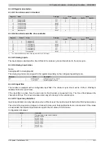
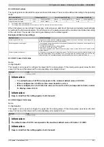
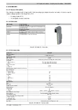
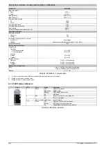
4.3.8.3 Technical data
Product ID
X20AI2622
Short description
I/O module
2 analog inputs ±10 V or 0 to 20 mA / 4 to 20 mA
General information
B&R ID code
0x1B9E
Status indicators
I/O function per channel, operating state, module status
Diagnostics
Module run/error
Yes, using status LED and software
Inputs
Yes, using status LED and software
Channel type
Yes, using software
Power consumption
Bus
0.01 W
Internal I/O
0.8 W
1)
Additional power dissipation caused by the actua-
tors (resistive) [W]
-
Electrical isolation
Channel - Bus
Yes
Channel - Channel
No
Certification
CE
Yes
cULus
Yes
cCSAus HazLoc Class 1 Division 2
Yes
ATEX Zone 2
Yes
KC
Yes
GOST-R
Yes
Analog inputs
Input
±10 V or 0 to 20 mA / 4 to 20 mA, via different connection terminal points
Input type
Differential input
Digital converter resolution
Voltage
±12-bit
Current
12-bit
Conversion time
300 µs for all inputs
Output format
INT
Output format
Voltage
INT 0x8001 - 0x7FFF / 1 LSB = 0x0008 = 2.441 mV
Current
INT 0x0000 - 0x7FFF / 1 LSB = 0x0008 = 4.883 µA
Input impedance in signal range
Voltage
20 MΩ
Current
-
Load
Voltage
-
Current
<400 Ω
Input protection
Protection against wiring with supply voltage
Permitted input signal
Voltage
Max. ±30 V
Current
Max. ±50 mA
Output of the digital value during overload
Below lower limit
Voltage
0x8001
Current
0x0000
Above upper limit
Voltage
0x7FFF
Current
0x7FFF
Conversion procedure
SAR
Input filter
3rd-order low pass / cutoff frequency 1 kHz
Max. error at 25°C
Voltage
Gain
0.08%
2)
Offset
0.015%
3)
Current
Gain
0 to 20 mA = 0.08% / 4 to 20 mA = 0.1%
2)
Offset
0 to 20 mA = 0.03% / 4 to 20 mA = 0.16%
4)
Max. gain drift
Voltage
0.006 %/°C
2)
Current
0 to 20 mA = 0.009 %/°C
4 to 20 mA = 0.0113 %/°C
2)
Max. offset drift
Voltage
0.002 %/°C
3)
Current
0 to 20 mA = 0.004 %/°C
4 to 20 mA = 0.005 %/°C
4)
Common-mode rejection
DC
70 dB
50 Hz
70 dB
Common-mode range
±12 V
Table 51: X20AI2622 - Technical data


