3. OPERATION AND TIMING
COPYRIGHT © 2001 CANON INC. CANON CLC1000/1000S/3100 REV.2 MAY 2001 PRINTED IN JAPAN (IMPRIME AU JAPON)
3-38
C. Analog Image Processing
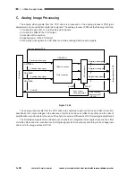
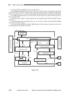
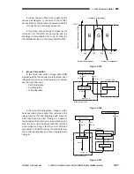
The analog video signals from the CCD driver is processed on the analog processor PCB (gain
adjustment) and converted into digital video signals. The analog processor PCB has the following functions:
1 Corrects the gain of R, G, and B analog video signals.
2 Corrects the offset in the CCD output.
3 Executes A/D conversion.
4 Supplies power to the CCD driver.
5 Generates clock signals for CCD driver and main scanning direction sync signals.
Figure 3-304
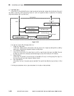
The analog video signals from the CCD driver are subjected to gain correction and offset correction:
specifically, the output voltages in the absence of light are made even (offset correction) and the ratio of
amplification is made constant to even out the photo-conversion efficiencies of CCD pixels (gain adjustment)
The RGB video signals of the odd and even channels are integrated into a single channel in the offset
correction block and are converted into 8-bit digital signals (A/D conversion) according to the voltage level
and sent to the image processor PCB.
Image processor PCB
CCD driver
R analog video signal
ODD,EVEN
ODD,EVEN
ODD,EVEN
ODD,EVEN
R digital video signal
G analog video signal
B analog video signal
Analog processor PCB
A/D conversion
8
G digital video signal
8
B digital video signal
8
Sync control
clock generation
Main scanning
direction signal
(HSYNC)
SH/SEL
CLK/SP
ADCLK
Gain correction
Offset correction
Summary of Contents for Vizcam 1000
Page 12: ......
Page 30: ......
Page 44: ......
Page 86: ......
Page 254: ......
Page 372: ......
Page 374: ......
Page 418: ......
Page 438: ......
Page 442: ......
Page 754: ......
Page 764: ......
Page 766: ......
Page 840: ...0501GR PRINTED IN JAPAN IMPRIME AU JAPON This publication is printed on 100 reprocessed paper...

