POM Control Registers
676
SPNU503C – March 2018
Copyright © 2018, Texas Instruments Incorporated
Parameter Overlay Module (POM)
18.3.1 POM Global Control Register (POMGLBCTRL)
This register contains a key to enable the POM module. Logic remains reset until this key is set.
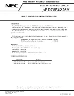
Figure 18-3. POM Global Control Register (POMGLBCTRL) [address = FFA0 4000h]
31
23
22
16
OTADDR
Reserved
R/WP-60h
R-0
15
12
11
8
7
4
3
0
Reserved
ETO
Reserved
ON/OFF
R-0
R/WP-5h
R-0
R/WP-5h
LEGEND: R/W = Read/Write; R = Read only; WP = Write in privilege mode only; -
n
= value after reset
Table 18-2. POM Global Control Register (POMGLBCTRL) Field Descriptions
Bit
Field
Value
Description
31-23
OTADDR
60h
Overlay target Address
.
These bits determine the upper address bits of the target overlay address. Writing a different
value to this field will steer the POM access to a different location in the 4GB address space.
The application must ensure that the overlay memory address points to a valid internal or
external memory location.
22-12
Reserved
0
Reads return 0, writes have no effect.
11-8
ETO
Enable Timeout
. Refer to
for more details on the timeout error.
Ah
Timeout for bus transactions is enabled.
All other values
Timeout for bus transactions is disabled. The timeout is disabled by default.
7-4
Reserved
0
Reads return zeros, writes have no effect.
3-0
ON/OFF
Turn functionality of POM on or off.
Ah
POM is functional.
All other values
POM is held in reset.
NOTE: The key should be written to 5h, to avoid single bit flips inadvertently turning on the
module.