background image

MOS INTEGRATED CIRCUIT

µ

PD78F4225Y

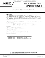
16/8-BIT SINGLE-CHIP MICROCONTROLLERS

DESCRIPTION

The 

µ

PD78F4225Y is a product in the 

µ

PD784225Y subseries in the 78K/IV series.

The 

µ

PD78F4225Y has a flash memory in the place of the internal ROM of the 

µ

PD784225Y.  Data can be written

to or erased from the flash memory of the 

µ

PD78F4225F with the microcontroller mounted on a printed wiring board.

The 

µ

PD78F4225Y is based on the 

µ

PD78F4225 with an I

2

C bus control function appended, and is ideal for

applications in audio visual.

The functions are explained in detail in the following user’s manuals.  Be sure to read this manual when

designing your system.

µ

PD784225, 784225Y Subseries User’s Manual - Hardware :  Planned

78K/IV Series User’s Manual - Instruction

:  U10905E

FEATURES

I

2

C bus serial interface supporting multi task

Pin-compatible with mask ROM model (except V

PP

 pin)

Flash memory:  128K bytes

Internal RAM :  4352 bytes

Same operating voltage as mask ROM model:  V

DD

 = 1.8 to 5.5 V

ORDERING INFORMATION

Part Number

Package

µ

PD78F4225YGC-8BT

80-pin plastic QFP (14 

×

 14 mm)

µ

PD78F4225YGK-BE9

80-pin plastic TQFP (fine pitch) (12 

×

 12 mm)

Document No. U12377EJ1V0PM00 (1st edition)
Date Published May 1997 N
Printed in Japan

The information contained in this document is being issued in advance of the production cycle for the
device.  The parameters for the device may change before final production or NEC Corporation, at its own
discretion, may withdraw the device prior to its production.

©

1997

PRELIMINARY  PRODUCT  INFORMATION

Содержание uPD78F4225Y

Страница 1: ...5 784225Y Subseries User s Manual Hardware Planned 78K IV Series User s Manual Instruction U10905E FEATURES I2C bus serial interface supporting multi task Pin compatible with mask ROM model except VPP...

Страница 2: ...d internal memory capacity pin compatible with PD784026 I2 C bus compatible model Under mass production Under development Multi master I2 C bus compatible model Multi master I2 C bus compatible model...

Страница 3: ...ve output 8 bit timer counter 5 timer register 1 Compare register 1 8 bit timer counter 6 timer register 1 Compare register 1 Serial interface UART IOE 3 wire serial I O 2 channels on chip baud rate g...

Страница 4: ...han Port Pins 11 4 3 I O Circuit Type of Respective Pins and Recommended Connections of Unused Pins 13 5 INTERNAL MEMORY SIZE SELECT REGISTER IMS 16 6 FLASH MEMORY PROGRAMMING 17 6 1 Selecting Communi...

Страница 5: ...sh memory instead of the mask ROM of the above models These differences are summarized in Table 1 1 Table 1 1 Differences among Models in PD784225Y Subseries Part Number PD784224Y PD784225Y PD78F4225Y...

Страница 6: ...P70 SI2 RxD2 P71 SO2 TxD2 P72 SCK2 ASCK2 P20 SI1 RxD1 P21 SO1 TxD1 P22 SCK1 ASCK1 P23 PCL P24 BUZ P25 SI0 SDA0 P26 SO0 P27 SCK0 SCL0 P40 AD0 P41 AD1 60 59 58 57 56 55 54 53 52 51 50 49 48 47 46 45 44...

Страница 7: ...7 Port1 P20 P27 Port2 P30 P37 Port3 P40 P47 Port4 P50 P57 Port5 P60 P67 Port6 P70 P72 Port7 P120 P127 Port12 P130 P131 Port13 PCL Programmable Clock RD Read Strobe RESET Reset RTP0 RTP7 Real time Outp...

Страница 8: ...D AVSS PCL BUZ ANI0 ANI7 D A CONVERTER ANO0 AVSS AVREF1 ANO1 78K IV CPU CORE FLASH MEMORY RAM BAUD RATE GENERATOR RxD1 SI1 TxD1 SO1 ASCK1 SCK1 RxD2 SI2 TxD2 SO2 ASCK2 SCK2 SI0 SDA0 SO0 SCK0 SCL0 BUS I...

Страница 9: ...ware Can drive LEDs P50 P57 I O A8 A15 Port 5 P5 8 bit I O port Can be set in input or output mode bit wise All pins set in input mode can be connected to internal pull up resistors by software Can dr...

Страница 10: ...nput mode can be connected to internal pull up resistor by software bit wise P130 P131 I O ANO0 ANO1 Port 13 P13 2 bit I O port Can be set in input or output mode bit wise Port 6 P6 8 bit I O port Can...

Страница 11: ...wire serial I O0 SO1 P21 TxD1 Serial data output 3 wire serial I O1 SO2 P71 TxD2 Serial data output 3 wire serial I O2 SDA0 I O P25 SI0 Serial data input output I2C bus SCK0 I O P27 SCL0 Serial clock...

Страница 12: ...scillation crystal XT2 ANI0 ANI7 Input P10 P17 Analog voltage input for A D converter ANO0 ANO1 Output P130 P131 Analog voltage output for D A converter AVREF1 To apply reference voltage for D A conve...

Страница 13: ...O Recommended Connections of Unused Pins P00 INTP0 8 C I O Input Individually connected to VSS0 via resistor P01 INTP1 Output Open P02 INTP2 NMI P03 INTP3 P05 INTP5 P10 ANI0 P17 ANI7 9 Input Connecte...

Страница 14: ...Recommended Connections of Unused Pins RESET 2 Input XT1 16 Connected to VSS0 XT2 Open AVREF1 Connected to VDD0 AVDD AVSS Connected to VSS0 TEST VPP Directly connected to VSS0 Remark Because the circu...

Страница 15: ...8 C pullup enable data output disable VDD0 P ch VDD0 P ch IN OUT N ch Type 9 pullup enable data open drain output disable VDD0 P ch VDD0 P ch IN OUT N ch Type 10 B Type 12 C pullup enable data output...

Страница 16: ...ernal Memory Size Select Register IMS Caution IMS is not provided on the mask ROM models PD784224Y and 784225Y The value to be set to the IMS to map the memory of the PD78F4225Y in the same manner as...

Страница 17: ...er of VPP pulses shown in Table 6 1 Table 6 1 Communication Modes Communication Mode Number of Channels Pins Used Number of VPP Pulses 3 wire serial I O 3 SCK0 SCL0 P27 0 SO0 P26 SI0 SDA0 P25 SCK1 ASC...

Страница 18: ...s erased status of specified block Data write Writes flash memory based on write start address and number of data to be written in bytes Batch verify Compares all contents of memory with input data Bl...

Страница 19: ...o 3 Wire Serial I O Mode Flashpro II PD78F4225Y VPPnNote VDD VSS RESET SCK SI VPP VDD0 VDD1 VSS0 VSS1 RESET SCL0 SDA0 Note n 1 2 Flashpro II PD78F4225Y VPPnNote VDD VSS RESET SO SI VPP VDD0 VDD1 VSS0...

Страница 20: ...009 0 008 S 1 70 MAX 0 067 MAX M 0 17 0 007 0 001 0 003 0 03 0 07 0 009 0 008 C 14 00 0 20 0 551 0 009 0 008 A 17 20 0 20 0 677 0 008 G 0 825 0 032 H 0 32 0 06 0 013 0 002 0 003 I 0 13 0 005 J 0 65 T...

Страница 21: ...14 0 0 2 0 551 0 009 0 008 B 12 0 0 2 0 472 0 009 0 008 C 12 0 0 2 0 472 0 009 0 008 D 14 0 0 2 0 551 0 009 0 008 F G 1 25 1 25 0 049 0 049 H 0 22 0 009 0 002 P80GK 50 BE9 4 S 1 27 MAX 0 050 MAX K 1...

Страница 22: ...series IE 784218 R EM1 Emulation board for evaluation of PD784225Y subseries IE 784000 R EM IE 70000 98 IF B Interface adapter when PC 9800 series except notebook type is used as host machine IE 7000...

Страница 23: ...e 2 PC 9800 series MS DOS Windows base IBM PC AT and compatible machine PC DOS Windows MS DOS IBM DOS base HP9000 series 700 HP UX base SPARCstation SunOS base 3 PC 9800 series MS DOS base IBM PC AT a...

Страница 24: ...Documents related to development tools User s Manuals Document Name Document No Japanese English RA78K4 Assembler Package Operation U11334J U11334E Language U11162J RA78K Series Structured Assembler P...

Страница 25: ...nductor Device Mounting Technology Manual C10535J C10535E Quality Grades on NEC Semiconductor Devices C11531J C11531E NEC Semiconductor Device Reliability Quality Control System C10983J C10983E Electr...

Страница 26: ...26 PD78F4225Y MEMO...
Страница 27: ...on for CMOS device inputs can be cause of malfunction If no connection is provided to the input pins it is possible that an internal input level may be generated due to noise etc hence causing malfunc...

Страница 28: ...l 040 2445845 Fax 040 2444580 NEC Electronics France S A Velizy Villacoublay France Tel 01 30 67 58 00 Fax 01 30 67 58 99 NEC Electronics France S A Spain Office Madrid Spain Tel 01 504 2787 Fax 01 50...

Страница 29: ...Standard Specification as defined by Philips IEBus is a trademark of NEC Corp MS DOS and Windows are trademarks of Microsoft Corp IBM DOS PC AT and PC DOS are trademarks of IBM Corp HP9000 series 700...

Страница 30: ...ti failure features NEC devices are classified into the following three quality grades Standard Special and Specific The Specific quality grade applies only to devices developed based on a customer de...

Отзывы: