


FlexRay Communication Controller (FLEXRAY)
22-14
Freescale Semiconductor
PXR40 Microcontroller Reference Manual, Rev. 1
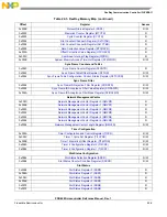
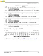
Table 22-8. MCR Field Descriptions
Field
Description
MEN
Module Enable — This bit indicates whether or not the controller is in the Disabled Mode. The application
requests the controller to leave the Disabled Mode by writing 1 to this bit Before leaving the Disabled Mode, the
application must configure the SCM, SBFF, CHB, CHA, TMODE, BITRATE values. For details see
Section 22.1.6, Modes of Operation
0 Write: ignored, controller disable not possible
Read: controller disabled
1 Write: enable controller
Read: controller enabled
Note: If the controller is enabled it can not be disabled.
SBFF
System Bus Failure Freeze — This bit controls the behavior of the controller in case of a system bus failure.
0 Continue normal operation
1 Transition to freeze mode
SCM
Single Channel Device Mode — This control bit defines the channel device mode of the controller as described
in
Section 22.6.10, Channel Device Modes
.
0 controller works in dual channel device mode
1 controller works in single channel device mode
CHB
CHA
Channel Enable — protocol related parameter:
pChannels
The semantic of these control bits depends on the channel device mode controlled by the SCM bit and is given
.
SFFE
Synchronization Frame Filter Enable — This bit controls the filtering for received synchronization frames. For
details see
Section 22.6.15, Sync Frame Filtering
0 Synchronization frame filtering disabled
1 Synchronization frame filtering enabled
R*
Reserved — This bit is reserved. It is read as 0. Application must not write 1 to this bit.
FUM
FIFO Update Mode — This bit controls the FIFO update behavior when the interrupt flags GIFER[FAFAIF] and
DIFER[FAFBIF] are written by the application (see
0 FIFOA (FIFOB) is updated on writing 1 to GIFER[FAFAIF] (GIFER[FAFBIF])
1 FIFOA (FIFOB) is not updated on writing 1 to GIFER[FAFAIF] (GIFER[FAFBIF])
FAM
FIFO Address Mode — This bit controls the location of the system memory base address for the FIFOs. (see
Section 22.6.9.2, FIFO Configuration
).
0 FIFO Base Address located in
System Memory Base Address Register (SYMBADR)
1 FIFO Base Address located in
Receive FIFO System Memory Base Address Register (RFSYMBADR)
CLKSEL
Protocol Engine Clock Source Select — This bit is used to select the clock source for the protocol engine.
0 PE clock source is generated by on-chip crystal oscillator.
1 PE clock source is generated by on-chip PLL.
BITRATE
FlexRay Bus Bit Rate — This bit field defines the FlexRay Bus Bit Rate.00010.0 Mbit/sec
001 5.0 Mbit/sec
010 2.5 Mbit/sec
011 8.0 Mbit/sec
100 reserved
101 reserved
110 reserved
111 reserved
Summary of Contents for PXR4030
Page 1: ...PXR40 Microcontroller Reference Manual Devices Supported PXR4030 PXR4040 PXR40RM Rev 1 06 2011...
Page 30: ...PXR40 Microcontroller Reference Manual Rev 1 Freescale Semiconductor xxx...
Page 40: ...PXR40 Microcontroller Reference Manual Rev 1 xl Freescale Semiconductor...
Page 66: ...Memory Map PXR40 Microcontroller Reference Manual Rev 1 2 4 Freescale Semiconductor...
Page 120: ...Signal Descriptions 3 54 Freescale Semiconductor PXR40 Microcontroller Reference Manual Rev 1...
Page 860: ...FlexCAN Module 24 50 Freescale Semiconductor PXR40 Microcontroller Reference Manual Rev 1...
Page 1167: ...Decimation Filter Freescale Semiconductor 28 53 PXR40 Microcontroller Reference Manual Rev 1...
Page 1168: ...Decimation Filter 28 54 Freescale Semiconductor PXR40 Microcontroller Reference Manual Rev 1...


