


Enhanced Direct Memory Access Controller (eDMA)
21-42
Freescale Semiconductor
PXR40 Microcontroller Reference Manual, Rev. 1
21.4.1
eDMA Basic Data Flow
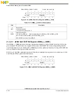
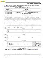
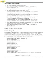
The eDMA transfers data based on a two-deep, nested flow. The basic flow of a data transfer can be
partitioned into three segments. As shown in
, the first segment involves the channel service
request. In the diagram, this example uses the assertion of the eDMA peripheral request signal to request
service for channel
n
. Channel service request via software and the TCDn.START bit follows the same
basic flow as an eDMA peripheral request. The eDMA peripheral request input signal is registered
internally and then routed through the DMA engine, first through the control module, then into the
program model/channel arbitration module. In the next cycle, the channel arbitration is performed using
the fixed-priority or round-robin algorithm. After the arbitration is complete, the activated channel number
is sent through the address path and converted into the required address to access the TCD local memory.
Next, the TCD memory is accessed and the required descriptor read from the local memory and loaded
into the DMA engine address path channel {x,y} registers. The TCD memory is organized 64-bits in width
to minimize the time needed to fetch the activated channel’s descriptor and load it into the eDMA engine
address path channel {x,y} registers.
Figure 21-25. eDMA Operation, Part 1
In the second part of the basic data flow as shown in
, the modules associated with the data
transfer (address path, data path, and control) sequence through the required source reads and destination
writes to perform the actual data movement. The source reads are initiated and the fetched data is
Sl
ave
in
te
rf
ace
eDMA
eDMA peripheral request
System bus
Data path
Control
Address
Program model/
Slave write data
Slave write address
Bus write data
Slave read data
Bus address
eDMA engine
TCD0
TCD
n
– 1*
eDMA interrupt request
Bus read data
channel arbitration
eDMA done handshake
path
SRAM
Transfer control descriptor
(
TCD
)
SRAM
*n = 32 (64 for eDMA_A) channels
Summary of Contents for PXR4030
Page 1: ...PXR40 Microcontroller Reference Manual Devices Supported PXR4030 PXR4040 PXR40RM Rev 1 06 2011...
Page 30: ...PXR40 Microcontroller Reference Manual Rev 1 Freescale Semiconductor xxx...
Page 40: ...PXR40 Microcontroller Reference Manual Rev 1 xl Freescale Semiconductor...
Page 66: ...Memory Map PXR40 Microcontroller Reference Manual Rev 1 2 4 Freescale Semiconductor...
Page 120: ...Signal Descriptions 3 54 Freescale Semiconductor PXR40 Microcontroller Reference Manual Rev 1...
Page 860: ...FlexCAN Module 24 50 Freescale Semiconductor PXR40 Microcontroller Reference Manual Rev 1...
Page 1167: ...Decimation Filter Freescale Semiconductor 28 53 PXR40 Microcontroller Reference Manual Rev 1...
Page 1168: ...Decimation Filter 28 54 Freescale Semiconductor PXR40 Microcontroller Reference Manual Rev 1...


